

Page 1
STEVAL-TDR015V1
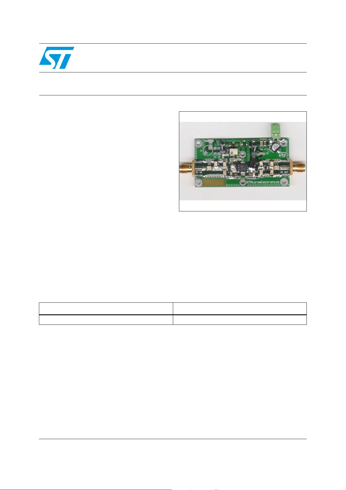
Demonstration board using the PD54008L-E for 2-way UHF radio
Features
■ Excellent thermal stability
■ Frequency: 400 - 470 MHz
■ Supply voltage: 7.2 V
■ Output power: 8 W
■ Power gain: 12.0 ± 1.0 dB
■ Efficiency: 56 % - 68 %
■ Load mismatch: 20:1
■ BeO-free amplifier
Description
The STEVAL-TDR015V1 is a demonstration
board using the PD54008L-E LDMOS transistor.
It is designed for 2-way UHF portable radio
applications.
Table 1. Device summary
Part number Mechanical specification
STEVAL-TDR015V1 L = 60 mm, W = 30 mm
October 2010 Doc ID 18095 Rev 1 1/12
www.st.com
12
Page 2

Contents STEVAL-TDR015V1
Contents
1 Electrical characteristics . . . . . . . . . . . . . . . . . . . . . . . . . . . . . . . . . . . . . 3
2 Impedance . . . . . . . . . . . . . . . . . . . . . . . . . . . . . . . . . . . . . . . . . . . . . . . . . 4
3 Typical performance . . . . . . . . . . . . . . . . . . . . . . . . . . . . . . . . . . . . . . . . . 5
4 Test circuit . . . . . . . . . . . . . . . . . . . . . . . . . . . . . . . . . . . . . . . . . . . . . . . . . 7
5 Circuit layout . . . . . . . . . . . . . . . . . . . . . . . . . . . . . . . . . . . . . . . . . . . . . . . 9
6 Revision history . . . . . . . . . . . . . . . . . . . . . . . . . . . . . . . . . . . . . . . . . . . 10
2/12 Doc ID 18095 Rev 1
Page 3
STEVAL-TDR015V1 Electrical characteristics
1 Electrical characteristics
TA = +25 °C, VDD = 7.5 V, I
= 50 mA
dq
Table 2. Electrical specifications
Symbol Test conditions Min. Typ. Max. Unit
Freq Frequency range 400 470 MHz
P
OUT
Gain @ P
ND @ P
H2 2nd harmonic @ P
H3 3rd harmonic @ P
= 8 W 12.0 ± 1.0 dB
OUT
= 8 W 56 - 68 %
OUT
= 8 W -28 / -44 dBc
OUT
= 8 W -58 / -61 dBc
OUT
VSWR Load mismatch all phases @ P
= 8 W 20:1
OUT
78 W
Doc ID 18095 Rev 1 3/12
Page 4

Impedance STEVAL-TDR015V1
2 Impedance
Figure 1. Impedance illustration
Z
IN
Z
GS
Table 3. Impedance data
D
G
S
ZDL
F (MHz) Z
GS
Z
DL
400 1.588 + j3.459 2.128 + j1.795
410 1.772 + j3.516 2.175 + j2.026
420 1.912 + j3.440 2.236 + j2.266
430 1.827 + j3.236 2.304 + j2.465
440 1.432 + j3.145 2.341 + j2.630
450 0.982 + j3.368 2.385 + j2.771
460 0.682 + j3.742 2.422 + j2.844
470 0.521 + j4.204 2.410 + j2.888
4/12 Doc ID 18095 Rev 1
Page 5

STEVAL-TDR015V1 Typical performance
3 Typical performance
Figure 2. Output power vs. input power Figure 3. Gain and efficiency vs.
14
16
output power Freq = 400 Mhz
80
12
10
8
6
Pout(W)
4
Vdd = 7.2V
2
0
0.0 0.2 0. 4 0.6 0.8 1.0
Idq = 50mA
Pin(W)
400MHz 435MHz 470MHz
Figure 4. Gain and efficiency vs.
16
14
12
10
output power Freq = 435 Mhz
80
70
60
50
14
12
10
8
Gain(dB)
6
4
2
0
024681012
Freq =400MHz
Vdd = 7.2V
Idq = 50mA
Pout(W)
Gain Nd
Figure 5. Gain and efficiency vs.
output power Freq = 470 Mhz
16
14
12
10
70
60
50
40
Drain Eff(%)
30
20
10
0
80
70
60
50
8
Gain(dB)
6
4
2
0
024681012
Freq =435MHz
Vdd = 7.2V
Idq = 50mA
Pout(W)
Gain Nd
Doc ID 18095 Rev 1 5/12
40
30
20
10
0
8
Gain(dB)
Drain Eff(%)
6
4
2
0
024681012
Freq =470MHz
Vdd = 7.2V
Idq = 50mA
40
Drain Eff(%)
30
20
10
0
Pout(W)
Gai n Nd
Page 6

Typical performance STEVAL-TDR015V1
Figure 6. Gain and efficiency vs frequency
P
= 7 W
14
14
13
13
12
12
11
11
10
10
9
9
Gain (dB)
Gain (dB)
8
8
7
7
6
6
390 400 410 420 430 440 450 460 470 480
390 400 410 420 430 440 450 460 470 480
Figure 8. Input return loss vs frequency Figure 9. Harmonics vs frequency
0.0
-2.0
-4.0
IRL(dB)
-6.0
-8.0
-10.0
390 400 410 420 430 440 450 460 470 480
OUT
Freq (MHz)
Freq (MHz)
Gain Nd
Gain Nd
Freq(MHz)
Pout = 7 W
Pout = 7 W
Vdd = 7.2 V
Vdd = 7.2 V
Idq = 50 mA
Idq = 50 mA
Pout =8W
Vdd = 7.2 V
Idq = 50mA
Figure 7. Gain and efficiency vs frequency
P
= 8 W
OUT
14
80
80
75
75
70
70
65
65
60
60
55
55
50
50
45
45
40
40
14
13
13
12
12
11
11
10
10
Gain (dB)
Gain (dB)
9
9
Drain Eff (%)
Drain Eff (%)
8
8
7
7
6
6
390 400 410 420 430 440 450 460 470 480
390 400 410 420 430 440 450 460 470 480
Freq (MHz)
Freq (MHz)
Gain Nd
Gain Nd
0
-10
-20
-30
-40
-50
Harmonics Level(dBc)
-60
-70
390 400 410 420 430 440 450 460 47 0 480
Freq(MHz)
H2 H3
Pout = 8 W
Pout = 8 W
Vdd = 7.2 V
Vdd = 7.2 V
Idq = 50 mA
Idq = 50 mA
Pout =8W
Vdd = 7.2 V
Idq = 50mA
80
80
75
75
70
70
65
65
60
60
55
55
Drain Eff (%)
Drain Eff (%)
50
50
45
45
40
40
6/12 Doc ID 18095 Rev 1
Page 7

STEVAL-TDR015V1 Typical performance
Figure 10. Output power vs drain voltage
14
12
10
8
6
Pout (W)
4
2
Idq = 50mA
Pin = 500mW
0
34567891011
Vdd (V)
400M Hz 435M Hz 470M Hz
Doc ID 18095 Rev 1 7/12
Page 8

Test circuit STEVAL-TDR015V1
4 Test circuit
Figure 11. Test circuit schematic
RF_in TL1
MSub
FR4
H=60mil
D1
C8
C6
TL2
C10
C9
L2
R3
R2
R1
C11
TL3
B2
C1
TL4
PD54008L
B1
C2
L1
C1 4
C1 3
L3
C1 2
TL5
C4 C5C3
C15
C16
L4
VDD
TL7
C7
Table 4. Part list
Component ID Description Value Case size Manufacturer Part code
C4 Capacitor 10 nF 1206 Murata GRM42-6X7R104K50
C3 Capacitor 1 nF 1206 Murata GRM42-6C0G102J50
=7.2V
RF_ O UTTL6
C1 Capacitor 120 pF 1206 Murata GRM42-6C0G121J50
C2 Capacitor 120 pF 1206 Murata GRM42-6C0G121J50
C6 Capacitor 120 pF 100B ATC 121
C7 Capacitor 120 pF 100B ATC 121
C8 Capacitor 2 pF 100B ATC 2R0
C9 Capacitor 13 pF 100B ATC 130
C10 Capacitor 20 pF 100B ATC 200
C11 Capacitor 62 pF 100A ATC 620
C12 Capacitor 43 pF 100A ATC 430
C13 Capacitor 4.3 pF 100B ATC 4R3
C14 Capacitor 15 pF 100B ATC 150
C15 Capacitor 3 pF 100B ATC 3R0
C16 Capacitor 6.8 pF 100B ATC 6R8
8/12 Doc ID 18095 Rev 1
Page 9

STEVAL-TDR015V1 Test circuit
Table 4. Part list (continued)
Component ID Description Value Case size Manufacturer Part code
C5 Capacitor 10 uF SMT Panasonic EEVHB1V100P
B2 Ferrite bead Panasonic EXCELDRC35C
B1 Ferrite bead Panasonic EXCELDRC35C
L1 Inductor 35.5 nH Coilcraft B09T
R2 Potentiometer 10 kΩ Bourns Electronics 3214W-1-103E
R3 Resistor 1 kΩ 1206 Tyco Electronics 01623440-1
R1 Resistor 15 Ω 1206 Tyco Electronics 01623429-1
RF in SMA-CONN Johnson 142-0701-801
RF out SMA-CONN Johnson 142-0701-801
TL1
TL2
TL3
Transmission
line
Transmission
line
Transmission
line
W=2.87 mm L=8.6 mm
W=2.87 mm L=11.7 mm
W=4.90 mm L=5.6 mm
TL4
TL5
TL6
TL7
D1 Zener diode 5.1 V SOD110 Philips BZX284C5V1
L2 2.55 nH 0906 Coilcraft 0906-3
L3 1.65 nH 0906 Coilcraft 0906-2
L4 3.85 nH 0906 Coilcraft 0906-4
PD54008L LDMOS STMicroelectronics PD54008L
Transmission
line
Transmission
line
Transmission
line
Transmission
line
W=4.90 mm L=5.8 mm
W=2.87 mm L=6.4 mm
W=2.87 mm L=4.5 mm
W=2.87 mm L=6.8 mm
Board: FR-4 THk=0.060" 2 OZ Cu both sides
Doc ID 18095 Rev 1 9/12
Page 10

Circuit layout STEVAL-TDR015V1
5 Circuit layout
Figure 12. Test fixture component layout
Figure 13. Test circuit photomaster
10/12 Doc ID 18095 Rev 1
Page 11

STEVAL-TDR015V1 Revision history
6 Revision history
Table 5. Document revision history
Date Revision Changes
14-Oct-2010 1 Initial release
Doc ID 18095 Rev 1 11/12
Page 12

STEVAL-TDR015V1
Please Read Carefully:
Information in this document is provided solely in connection with ST products. STMicroelectronics NV and its subsidiaries (“ST”) reserve the
right to make changes, corrections, modifications or improvements, to this document, and the products and services described herein at any
time, without notice.
All ST products are sold pursuant to ST’s terms and conditions of sale.
Purchasers are solely responsible for the choice, selection and use of the ST products and services described herein, and ST assumes no
liability whatsoever relating to the choice, selection or use of the ST products and services described herein.
No license, express or implied, by estoppel or otherwise, to any intellectual property rights is granted under this document. If any part of this
document refers to any third party products or services it shall not be deemed a license grant by ST for the use of such third party products
or services, or any intellectual property contained therein or considered as a warranty covering the use in any manner whatsoever of such
third party products or services or any intellectual property contained therein.
UNLESS OTHERWISE SET FORTH IN ST’S TERMS AND CONDITIONS OF SALE ST DISCLAIMS ANY EXPRESS OR IMPLIED
WARRANTY WITH RESPECT TO THE USE AND/OR SALE OF ST PRODUCTS INCLUDING WITHOUT LIMITATION IMPLIED
WARRANTIES OF MERCHANTABILITY, FITNESS FOR A PARTICULAR PURPOSE (AND THEIR EQUIVALENTS UNDER THE LAWS
OF ANY JURISDICTION), OR INFRINGEMENT OF ANY PATENT, COPYRIGHT OR OTHER INTELLECTUAL PROPERTY RIGHT.
UNLESS EXPRESSLY APPROVED IN WRITING BY AN AUTHORIZED ST REPRESENTATIVE, ST PRODUCTS ARE NOT
RECOMMENDED, AUTHORIZED OR WARRANTED FOR USE IN MILITARY, AIR CRAFT, SPACE, LIFE SAVING, OR LIFE SUSTAINING
APPLICATIONS, NOR IN PRODUCTS OR SYSTEMS WHERE FAILURE OR MALFUNCTION MAY RESULT IN PERSONAL INJURY,
DEATH, OR SEVERE PROPERTY OR ENVIRONMENTAL DAMAGE. ST PRODUCTS WHICH ARE NOT SPECIFIED AS "AUTOMOTIVE
GRADE" MAY ONLY BE USED IN AUTOMOTIVE APPLICATIONS AT USER’S OWN RISK.
Resale of ST products with provisions different from the statements and/or technical features set forth in this document shall immediately void
any warranty granted by ST for the ST product or service described herein and shall not create or extend in any manner whatsoever, any
liability of ST.
ST and the ST logo are trademarks or registered trademarks of ST in various countries.
Information in this document supersedes and replaces all information previously supplied.
The ST logo is a registered trademark of STMicroelectronics. All other names are the property of their respective owners.
© 2010 STMicroelectronics - All rights reserved
STMicroelectronics group of companies
Australia - Belgium - Brazil - Canada - China - Czech Republic - Finland - France - Germany - Hong Kong - India - Israel - Italy - Japan -
Malaysia - Malta - Morocco - Philippines - Singapore - Spain - Sweden - Switzerland - United Kingdom - United States of America
www.st.com
12/12 Doc ID 18095 Rev 1
 Loading...