


2 stage RF power amp: PD84001 + PD84008L-E + LPF
Features
■ Excellent thermal stability
■ Frequency: 400 - 470 MHz
■ Supply voltage: 7.2 V
■ Output power: 4 W
■ Current < 1.4 A
■ Input power < 10 dBm
■ Harmonics level < -70 dBc
■ Load mismatch 20:1
■ V
■ BeO-free amplifier
■ RoHS compliant
APC
5 V max
STEVAL-TDR006V1
N-channel enhancement-mode lateral MOSFETs
Mechanical specification:
L = 40 mm, W = 20 mm
Description
The STEVAL-TDR006V1 is a two stage RF power
amplifier which includes a low pass output filter for
harmonics rejection specifically designed for
portable two-way UHF radio communication.
Table 1. Device summary
Order code
STEVAL-TDR006V1
April 2009 Doc ID 15623 Rev 1 1/18
www.st.com
18

Contents STEVAL-TDR006V1
Contents
1 Electrical data . . . . . . . . . . . . . . . . . . . . . . . . . . . . . . . . . . . . . . . . . . . . . . 3
1.1 Maximum ratings . . . . . . . . . . . . . . . . . . . . . . . . . . . . . . . . . . . . . . . . . . . . 3
2 Electrical characteristics . . . . . . . . . . . . . . . . . . . . . . . . . . . . . . . . . . . . . 3
3 Typical performances . . . . . . . . . . . . . . . . . . . . . . . . . . . . . . . . . . . . . . . . 4
4 Circuit layout . . . . . . . . . . . . . . . . . . . . . . . . . . . . . . . . . . . . . . . . . . . . . . . 8
5 Circuit schematics . . . . . . . . . . . . . . . . . . . . . . . . . . . . . . . . . . . . . . . . . . 9
6 Package mechanical data . . . . . . . . . . . . . . . . . . . . . . . . . . . . . . . . . . . . 10
6.1 PowerFLAT™ mechanical data . . . . . . . . . . . . . . . . . . . . . . . . . . . . . . . . 11
6.1.1 Mounting indications . . . . . . . . . . . . . . . . . . . . . . . . . . . . . . . . . . . . . . . 14
6.2 Thermal pad and via design SOT-89 . . . . . . . . . . . . . . . . . . . . . . . . . . . . 15
6.2.1 Soldering profile . . . . . . . . . . . . . . . . . . . . . . . . . . . . . . . . . . . . . . . . . . . 16
7 Revision history . . . . . . . . . . . . . . . . . . . . . . . . . . . . . . . . . . . . . . . . . . . 18
2/18 Doc ID 15623 Rev 1
STEVAL-TDR006V1 Electrical data
1 Electrical data
1.1 Maximum ratings
Table 2. Absolute maximum ratings
Symbol Parameter Value Unit
V
T
CASE
DD
I
D
T
A
Supply voltage 15 V
Drain current 2.5 A
Operating case temperature -20 to +85 °C
Max. ambient temperature +55 °C
2 Electrical characteristics
TA = +25 °C, VDD = 7.2 V, V
Table 3. Electrical specification
Symbol Test conditions Min. Typ. Max. Unit
Freq. Frequency range 400 470 MHz
P
I
TOTAL
PA E @ P
VAPC @ P
Harmonics @ P
@ P
IN
@ P
= 4 W 10 dBm
OUT
= 4 W and PIN = 10 dBm 1.4 A
OUT
= 4 W and PIN = 10 dBm 42% - 45%
OUT
= 4 W and PIN = 10 dBm 4.5 5 V
OUT
= 4 W -70 dBc
OUT
APC
adjusted
Doc ID 15623 Rev 1 3/18
Typical performances STEVAL-TDR006V1
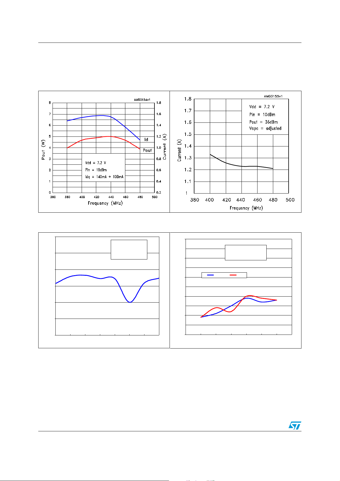
3 Typical performances
Figure 1. Output power and current vs
Figure 2. Supply current vs frequency
frequency
Figure 3. Input return loss vs frequency Figure 4. Harmonics vs frequency
0
Vdd = 7.2V
Pin = 10dBm
-4
Pout = 36dBm
Vapc = adjusted
-40
Vdd = 7.2V
Idq = 140mA + 100mA
-50
Pin = 10dBm
-8
-12
IRL (dB)
-16
-20
-24
380 400 420 440 460 480 50 0 520
Frequency (MHz)
4/18 Doc ID 15623 Rev 1
-60
-70
Harmonics (dB)
-80
-90
360 380 400 420 440 460 480 500
H2 H3
Frequency (MHz)

STEVAL-TDR006V1 Typical performances
Figure 5. Low pass filter - insertion loss
-5
-15
-25
-35
S21(dB)
-45
-55
-65
-75
1.0E +08 3.0E+08 5.0E+08 7.0E+08 9.0E+08 1. 1E+ 09 1.3E+09 1.5E+09
F(Hz)
Figure 6. Low pass filter - input return loss
0
Low pass filter - Input Return Loss
-5
-10
-15
-20
S11(dB)
-25
-30
-35
1.0E+08 3.0E+08 5.0E+08 7.0E+08 9.0E+08 1. 1E+09 1.3E+09 1.5E+09
F(Hz)
Doc ID 15623 Rev 1 5/18
Typical performances STEVAL-TDR006V1
Table 4. Parts list
Designator Value Quantity Manufacturer Part code Size
C1, C5, C6, C20 1 µF 4 EPCOS B45196E6105K209 CASE_B_TANT
C1F 2.2 pF 1 Murata GRM1885C1H2R2CZ01 603
C2, C3, C4 120 pF 3 Murata
GRM1885C1H121J,
GRM1885C1H121JA01
603
C2F, C3F 3.3 pF 2 Murata GRM1885C1H3R3CZ01 603
C4F, C5F 2.2 pF 2 Murata GRM1885C1H2R2CZ01 603
C6F 4.7 pF 1 Murata GRM1885C1H4R7CZ01 603
C7 100 nF 1 Murata GRM188R71E104K 603
C7F, C8F 3.9 pF 2 Murata GRM1885C1H3R9CZ01 603
C8, C10 470 pF 2 Murata GRM1885C1H471J 603
C9 470 pF 1 Murata GRM1885C1H471J 603
C9F 1.2 pF 1 Murata GRM1885C1H1R2CZ01 603
C11 9.1 pF 1 Murata CQM1885C1H9R1D 603
C13 22 pF 1 Murata GRM1885C1H220J 603
C14 33 pF 1 Murata GRM1885C1H330J 603
C15, C16 18 pF 2 Murata
CQM1885C1H180J,
GQM1885C1H180J
603
C17 8.2 pF 1 Murata CQM3295C2A8R2D 603
C19 9.1pF 1 Murata CQM1885C1H9R1D 603
DC-Con 5 poli 1 Phoenix Contact 1725685 2.54mm, 5 poli
L1 24 nH 1 Coilcraft 0603HC-24NXJLW 603
L1F, L2, L2F, L3F, L4F 12.5 nH 5 Coilcraft A04TJLB_12.5nH 1606
L3 7.5 nH 1 Coilcraft 0603HC-7N5X_BW 603
L4 1.6 nH 1 Coilcraft 0603HC-1N6XJLW 603
L5 5 nH 1 Coilcraft A02TJLC_5nH 1606
PD84001 LDMOS 1 STMicroelectronics PD84001
PD84008L LDMOS 1 STMicroelectronics PD84008L-E
R1 300 1
R2 3 K 1
R3, R6 16 2
R4 3.6 K 1
R5 8.2 K 1
Tyco/Electronics
Neohn
Tyco/Electronics
Neohn
Tyco/Electronics
Neohn
Tyco/Electronics
Neohn
Tyco/Electronics
Neohn
CRG Series Thick Film
Chip
CRG Series Thick Film
Chip
CRG Series Thick Film
Chip
CRG Series Thick Film
Chip
CRG Series Thick Film
Chip
6/18 Doc ID 15623 Rev 1
603
603
603
603
603
STEVAL-TDR006V1 Typical performances
Table 4. Parts list (continued)
Designator Value Quantity Manufacturer Part code Size
R7 11Ohm 1
RF In, RF Out, RF Out
PA
SUB 1 FR-4
Tyco/Electronics
Neohn
CRG Series Thick Film
Chip
603
SMA 3 Johnson SMA
H = 20mil
h = 1 oz
Doc ID 15623 Rev 1 7/18

Circuit layout STEVAL-TDR006V1
4 Circuit layout
Figure 7. Test fixture component layout
8/18 Doc ID 15623 Rev 1

STEVAL-TDR006V1 Circuit schematics
5 Circuit schematics
Figure 8. Circuit schematic
1_GND
C1
R2
C2
PD84001
2_Va pc1
3_Vd 1
4_Va pc2
5_Vd 2
12345
DC-Con
C15
C6
C7
L2
L5
C16
C19
C20
C3
L1
L4
C13
C5
R4
C4
R5
C9
R6
PD84008L
C14
C17
PB
1
2
C10
C18 (no conn..)
RF Out
RF Out PA
RF In
SUB
FR-4
H
H=20mil h=1oz
C8
C11
h
FR-4
R1
R3
L3
R7
Figure 9. Filter schematic
C1F
1 2
L1F
C5F
C6F
C2F
L2F
C7F
C3F
L3F
C8F
C4F
L4F
C9F
Doc ID 15623 Rev 1 9/18

Package mechanical data STEVAL-TDR006V1
6 Package mechanical data
In order to meet environmental requirements, ST offers these devices in different grades of
ECOPACK
®
packages, depending on their level of environmental compliance. ECOPACK®
specifications, grade definitions and product status are available at: www.st.com.
ECOPACK is an ST trademark.
10/18 Doc ID 15623 Rev 1

STEVAL-TDR006V1 Package mechanical data
6.1 PowerFLAT™ mechanical data
Table 5. PowerFLAT™ mechanical data
mm inch
Dim.
Min. Typ. Max. Min. Typ. Max.
A 0.90 1.00 0.035 0.039
A1 0.02 0.05 0.001 0.002
A3 0.24 0.009
AA 0.15 0.25 0.35 0.006 0.01 0.014
b 0.43 0.51 0.58 0.017 0.020 0.023
c 0.64 0.71 0.79 0.025 0.028 0.031
D 5.00 0.197
d 0.30 0.011
E 5.00 0.197
E2 2.49 2.57 2.64 0.098 0.101 0.104
e 1.27 0.050
f 3.37 0.132
g 0.74 0.03
h 0.21 0.008
Figure 10. PowerFLAT™ package dimensions
Doc ID 15623 Rev 1 11/18

Package mechanical data STEVAL-TDR006V1
Table 6. PowerFLAT™ tape and reel dimensions
mm. inch
Dim.
Min. Typ Max. Min. Typ Max.
Ao 5.15 5.25 5.35 0.12 0.13 0.13
Bo 5.15 5.25 5.35 0.12 0.13 0.13
Ko 1.0 1.1 1.2 0.02 0.02 0.02
Figure 11. PowerFLAT™ tape and reel
12/18 Doc ID 15623 Rev 1

STEVAL-TDR006V1 Package mechanical data
6.1.1 Mounting indications
Figure 12. Standard SMD mounting
Doc ID 15623 Rev 1 13/18

Package mechanical data STEVAL-TDR006V1
6.2 Thermal pad and via design SOT-89
Thermal vias are required in the PCB layout to effectively conduct heat away from the
package. The via pattern has been designed to address thermal, power dissipation and
electrical requirements of the device.
The via pattern is based on thru-hole vias with 0.203 mm to 0.330 mm finished hole size on
a 0.5 mm to 1.2 mm grid pattern with 0.025 plating on via walls. If micro vias are used in a
design, it is suggested that the quantity of vias be increased by a 4:1 ratio to achieve similar
results.
Figure 13. Pad layout details
14/18 Doc ID 15623 Rev 1
STEVAL-TDR006V1 Package mechanical data
6.2.1 Soldering profile
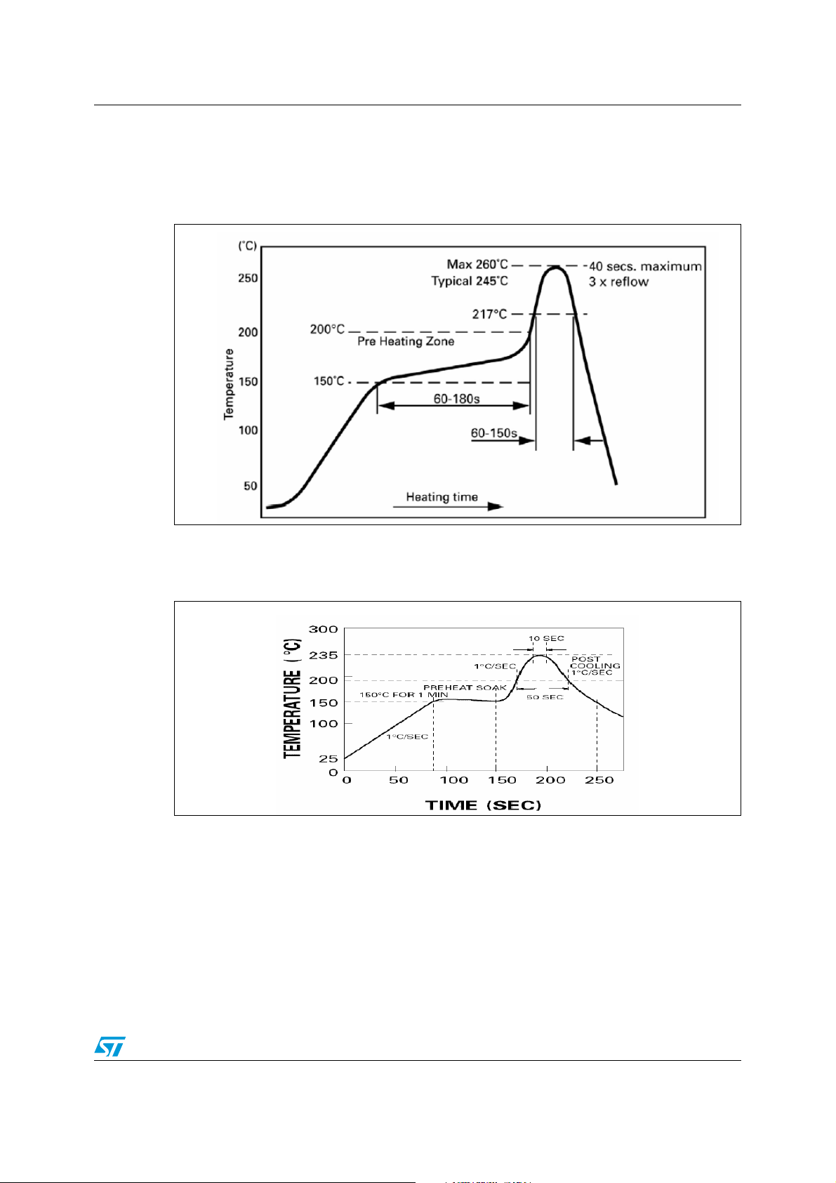
Figure 14 shows the recommeded solder for devices that have Pb-free terminal plating and
where a Pb-free solder is used.
Figure 14. Recommended solder profile
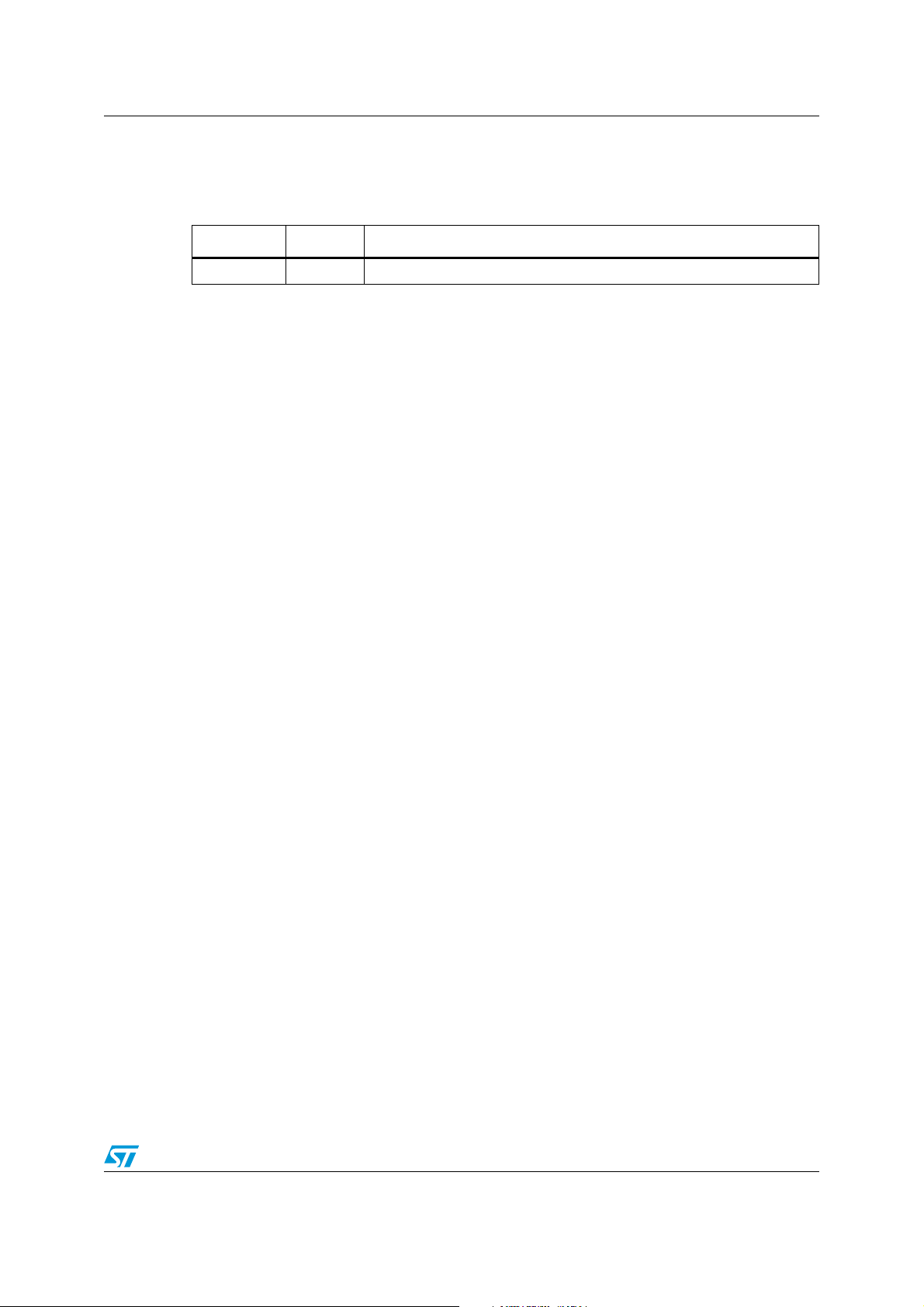
Figure 15 shows the recommeded solder for devices with Pb-free terminal plating used with
leaded solder, or for devices with leaded terminal plating used with a leaded solder.
Figure 15. Recommended solder profile for leaded devices
Doc ID 15623 Rev 1 15/18

Package mechanical data STEVAL-TDR006V1
Figure 16. Reel information
16/18 Doc ID 15623 Rev 1
STEVAL-TDR006V1 Revision history
7 Revision history
Table 7. Document revision history
Date Revision Changes
23-Apr-2009 1 Initial release.
Doc ID 15623 Rev 1 17/18

STEVAL-TDR006V1
y
y
Please Read Carefully:
Informatio n in this document is provided solely in connection with ST products. STMicroelectronics NV and its subsidiaries (“ST”) reserve the
right to make changes, corrections, modifications or improvements, to this document, and the products and services described herein at an
time, without notice.
All ST products are sold pursuant to ST’s terms and conditions of sale.
Purchasers are solely responsible for the choice, selection and use of the ST products and services described herein, and ST assumes no
liability whatsoever relating to the choice, selection or use of the ST products and services described herein.
No license, express or implied, by estoppel or otherwise, to any intellectual property rights is granted under this document. If any part of this
document refers to any third party products or services it shall not be deemed a license grant by ST for the use of such third party products
or services, or any intellectual property contained therein or considere d as a warranty covering the use in any manner whatsoever of such
third party products or services or any intellectual prope rty contained therein.
UNLESS OTHERWISE SET FORTH IN ST’S TERMS AND CONDITIONS OF SALE ST DISCLAIMS ANY EXPRESS OR IMPLIED
WARRANTY WITH RESPECT TO THE USE AND/OR SALE OF ST PRODUCTS INCLUDING WITHOUT LIMITATION IMPLIED
WARRANTIES OF MERCHANTABILITY, FITNESS FOR A PARTICULAR PURPOSE (AND THEIR EQUIVALENTS UNDER THE LAWS
OF ANY JURISDICTION), OR INFRINGEMENT OF ANY PATENT, COPYRIGHT OR OTHER INTELLECTUAL PROPERTY RIGHT.
UNLESS EXPRESSLY APPROVED IN WRITING BY AN AUTHORIZED ST REPRESENTATIVE, ST PRODUCTS ARE NOT
RECOMMENDED, AUTHORIZED OR WARRANTED FOR USE IN MILITARY, AIR CRAFT, SPACE, LIFE SAVING, OR LIFE SUSTAINING
APPLICATIONS, NOR IN PRODUCTS OR SYSTEMS WHERE FAILURE OR MALFUNCTION MAY RESULT IN PERSONAL INJURY,
DEATH, OR SEVERE PROPERTY OR ENVIRONMENTAL DAMAGE. ST PRODUCTS WHICH ARE NOT SPECIFIED AS "AUTOMOTIVE
GRADE" MAY ONLY BE USED IN AUTOMOTIVE APPLICATIONS AT USER’S OWN RISK.
Resale of ST products with provisions different from the statements and/or technical features set forth in this document shall immediately void
any warranty granted by ST for the ST product or service described herein and shall not create or extend in any manner whatsoever, an
liability of ST.
ST and the ST logo a re trademarks or registered trademarks of ST in various countries.
Information in this document supersedes and replaces all information previously supplied.
The ST logo is a registered trademark of STMicroelectronics. All other names are the property of their respective owners.
© 2009 STMicroelectronics - All rights reserved
STMicroelectronics group of companies
Australia - Belgium - Bra zil - Canada - China - Czech Republic - Finland - France - Germany - Hong Kong - India - Israel - Italy - Japan -
Malaysia - Malta - Morocco - Philippines - Singapore - Spain - Sweden - Switzerland - United Kingdom - United States of America
www.st.com
18/18 Doc ID 15623 Rev 1
 Loading...