

ST TDE3247 User Manual
Interface circuit (relay and lamp driver)
Features
■ High output current
■ Adjustable short-circuit protection to ground
■ Internal thermal protection with hysteresis to
avoid the intermediate output levels
■ Large supply voltage range: 8 to 30V
■ Short-circuit protection to V
■
Open ground protection
Description
The TDE3247 is a monolithic amplifier designed
for high current and high voltage applications,
specifically to drive lamps, relays and stepping
motors.
CC
TDE3247
SO-14
The Device is essentialy blow-out proof. Current
limiting is available to limit the peak output current
to a safe value, the adjustment only required an
external resistor.
In addition, thermal shut-down is provided to keep
the IC from overheating.
If external dissipation becomes too high, the
driver will shut-down to prevent excessive
heating.
The output is also protected against short-circuit
with the positive power supply.
The device operates over a wide range of supply
voltage from standard
supplies down to the single 12V or 24V used for
industrial electronic systems.
±15V operational amplifier
Order codes
Part number Package Packaging
TDE3247FP SO-14 Tube
TDE3247FPT SO-14 Tape & Reel
June 2006 Rev 2 1/15
www.st.com
15

Contents TDE3247
Contents
1 Schematic diagram and pin connections . . . . . . . . . . . . . . . . . . . . . . . . 3
2 Electrical ratings . . . . . . . . . . . . . . . . . . . . . . . . . . . . . . . . . . . . . . . . . . . . 4
3 Electrical characteristics . . . . . . . . . . . . . . . . . . . . . . . . . . . . . . . . . . . . . 5
3.1 Electrical characteristics (curves) . . . . . . . . . . . . . . . . . . . . . . . . . . . . . . 6
4 Application circuit . . . . . . . . . . . . . . . . . . . . . . . . . . . . . . . . . . . . . . . . . . . 8
5 Package mechanical data . . . . . . . . . . . . . . . . . . . . . . . . . . . . . . . . . . . . . 9
6 Revision history . . . . . . . . . . . . . . . . . . . . . . . . . . . . . . . . . . . . . . . . . . . 14
2/15
TDE3247 Schematic diagram and pin connections
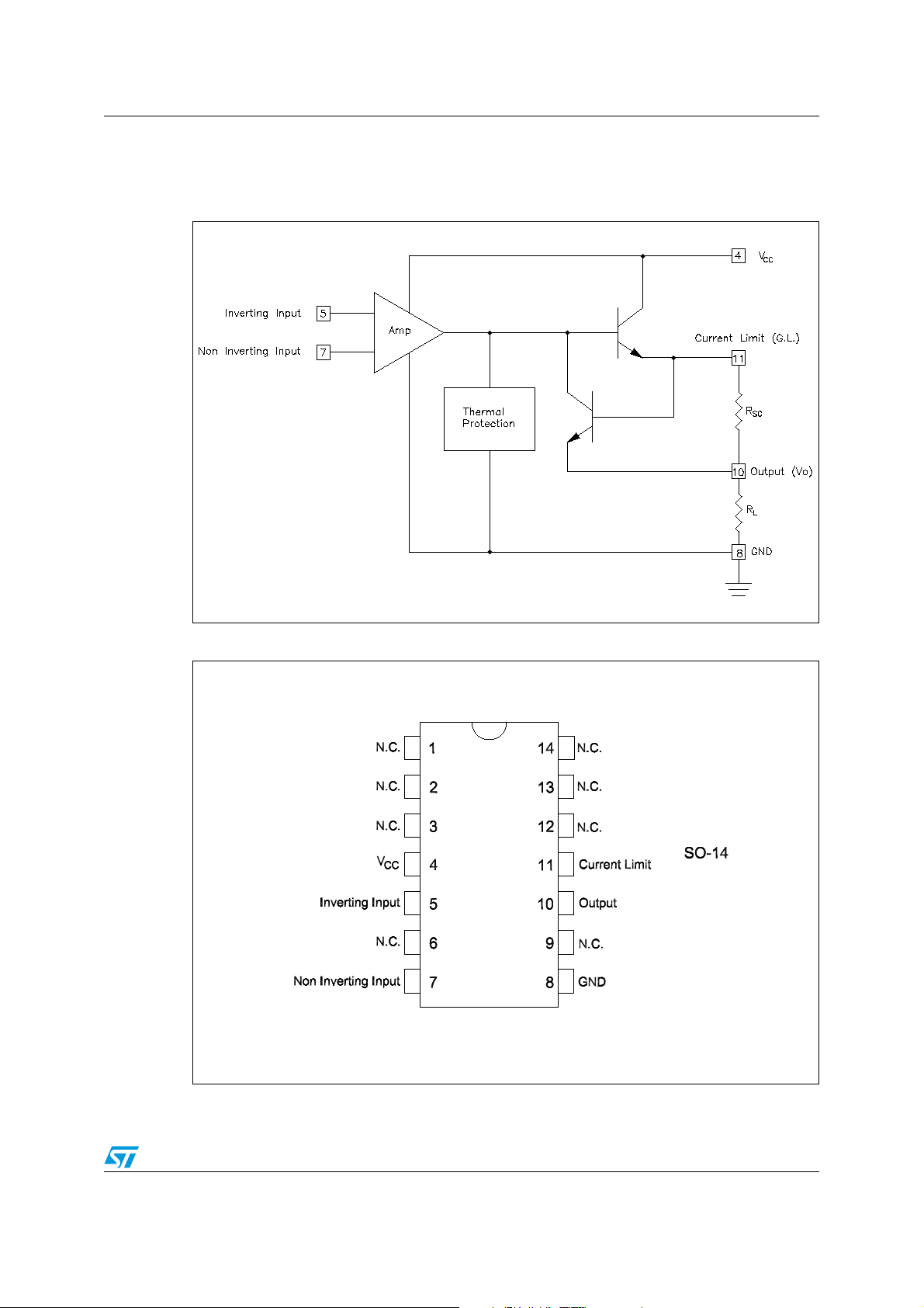
1 Schematic diagram and pin connections
Figure 1. Schematic diagram
Figure 2. Pin connections
3/15
Electrical ratings TDE3247
2 Electrical ratings
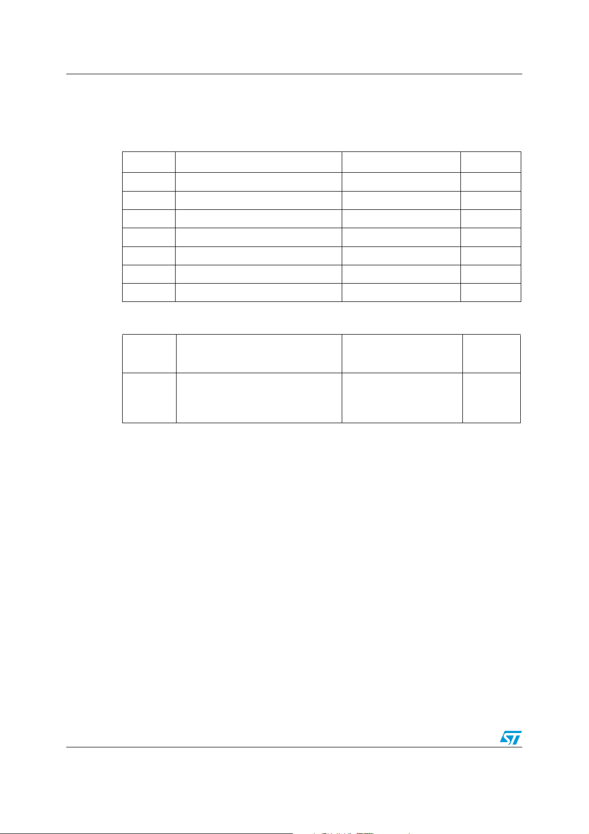
Table 1. Absolute maximum ratings
Symbol Parameter Value Unit
V
P
T
T
CC
V
V
I
O
TOT
oper
STG
Supply Voltage 36 V
Differential Input Voltage 36 V
O
Input Voltage 36 V
I
Output Current 300 mA
Power Dissipation Internally limited W
Ambient Temperature Range –25 to 85 ° C
Storage Temperature Range –65 to +150 ° C
Table 2. Thermal data
Junction-ceramic Substrate
R
th
R
th
(case glued to substrate)
For SO-14
Junction-ceramic Substrate
(case glued to substrate, substrate
temperature maintened constant)
For SO-14
90 °C/W
65 °C/W
4/15
TDE3247 Electrical characteristics
3 Electrical characteristics
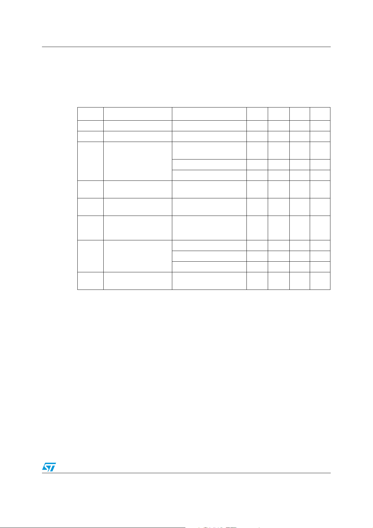
(-25°C ≤ TA 85°C, 8V ≤ V
CC
≤ 30V, I
≤ 150mA, TJ ≤ 150°C, unless otherwise specified) Note: 1
O
Table 3. Electrical characteristics
Symbol Parameter Test Conditions Min. Typ. Max. Unit
V
I
V
I
V
CC
I
Input Offset Voltage Note 2 250mV
IO
Input Bias Current 0.1 1.5 µA
I
IB
VCC = 24V, IO = 0A,
25°C
T
amb =
High Level 4 10 mA
CC
Supply Current
Low Level 2 mA
Common Mode Input
CM
Voltage Range
Short-circuit Current
SC
Output Saturation Voltage
- V
O
(Output High)
V
= 24V, T
CC
amb =
RSC = 3.3Ω
+
-
- V
(V
I
) ≤ 50mV
I
I
= 150mA, RSC = 0
O
TJ = 25°C
25°C
2V
CC
250 mA
1.2 1.8 V
VO = 0V, VCC = 24V
Output Leakage Current
I
OL
(Output Low)
Minimum Short-current
OS
Output Current
T
= 25°C 1 100 µA
J
= 85°C 500 µA
T
J
T
25°C, VCC = 24V
amb =
R
SC
= ∞
50 mA
-2 V
Note: 1 For operating at high temperatures, the device must be derated based on a 150°C
maximum junction and a junction to ambient thermal resistance of 110°C/W
2 The offset voltage given in the maximum value of input voltage required to drive the output
voltage within 2V of the ground or the supply voltage.
5/15
 Loading...