

Page 1
Car-radio multimedia signal processor (CMSP)
Features
■ 6-channel multimedia approach
■ Fully integrated tone control with notch filter
■ 7-band spectrum analyzer
Inputs
■ Three independent signal paths
■ Eight single-ended inputs
■ Two quasi-differential inputs
■ Optional full-differential input
■ Level adjust gain-stages
■ Independent soft-mute and direct-mute
Outputs
■ Three independent signal paths
■ Six output channels with soft-step volume
■ Output level up to 4VRMS
■ Independent soft-mute and direct-mute
■ Flexible phone/navigation interrupts
■ High-pass and subwoofer low-pass filters
Digital control
■ Selectable SPI- or I
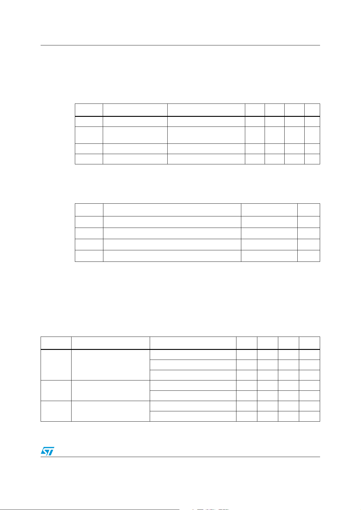
Table 1. Device summary
2
C-bus interface
TDA7415CB
LQFP64
Description
The TDA7415CB is the first 6-channel multimedia
approach in the car-radio signal processor (CSP)
family. It features full software programmability of
three independent sections. The signal processor
combines a three band audio tone control with an
additional notch filter, high/low pass filters for
subwoofer support and a spectrum-analyzer with
the absence of any external components for the
internal filters. Versatile input/output stages and an
extended signal routing scheme provide all the
flexibility that is needed to serve modern 6-channel
applications such as required by DVD technology.
Order code Temp range, °CPackage Packing
TDA7415CB -40 to 85 LQFP64 (10x10x1.4mm) Tray
June 2009 Doc ID 14100 Rev 3 1/50
www.st.com
1
Page 2

Contents TDA7415CB
Contents
1 Block diagram . . . . . . . . . . . . . . . . . . . . . . . . . . . . . . . . . . . . . . . . . . . . . . 6
2 Pin description . . . . . . . . . . . . . . . . . . . . . . . . . . . . . . . . . . . . . . . . . . . . . 7
2.1 ESD: . . . . . . . . . . . . . . . . . . . . . . . . . . . . . . . . . . . . . . . . . . . . . . . . . . . . . . 7
2.2 Thermal data . . . . . . . . . . . . . . . . . . . . . . . . . . . . . . . . . . . . . . . . . . . . . . . 7
2.3 Pin assignment . . . . . . . . . . . . . . . . . . . . . . . . . . . . . . . . . . . . . . . . . . . . . . 7
2.4 Pin function . . . . . . . . . . . . . . . . . . . . . . . . . . . . . . . . . . . . . . . . . . . . . . . . 8
3 Deatailed features . . . . . . . . . . . . . . . . . . . . . . . . . . . . . . . . . . . . . . . . . . 10
4 Electrical specification . . . . . . . . . . . . . . . . . . . . . . . . . . . . . . . . . . . . . . 11
4.1 Supply . . . . . . . . . . . . . . . . . . . . . . . . . . . . . . . . . . . . . . . . . . . . . . . . . . . 11
4.2 Absolute maximum ratings . . . . . . . . . . . . . . . . . . . . . . . . . . . . . . . . . . . . 11
4.3 Electrical characteristcs . . . . . . . . . . . . . . . . . . . . . . . . . . . . . . . . . . . . . . 11
4.3.1 Input section . . . . . . . . . . . . . . . . . . . . . . . . . . . . . . . . . . . . . . . . . . . . . 11
4.3.2 Main signal processing path . . . . . . . . . . . . . . . . . . . . . . . . . . . . . . . . . 13
4.3.3 Output section . . . . . . . . . . . . . . . . . . . . . . . . . . . . . . . . . . . . . . . . . . . . 15
4.3.4 General . . . . . . . . . . . . . . . . . . . . . . . . . . . . . . . . . . . . . . . . . . . . . . . . . 16
4.3.5 Bus and control inputs . . . . . . . . . . . . . . . . . . . . . . . . . . . . . . . . . . . . . . 17
4.3.6 DC offset detector . . . . . . . . . . . . . . . . . . . . . . . . . . . . . . . . . . . . . . . . . 17
5 Description of the audio processor . . . . . . . . . . . . . . . . . . . . . . . . . . . . 18
5.1 Input section . . . . . . . . . . . . . . . . . . . . . . . . . . . . . . . . . . . . . . . . . . . . . . . 18
5.2 Main signal processing path . . . . . . . . . . . . . . . . . . . . . . . . . . . . . . . . . . . 19
5.2.1 Bass filter . . . . . . . . . . . . . . . . . . . . . . . . . . . . . . . . . . . . . . . . . . . . . . . . 19
5.2.2 Mid filter . . . . . . . . . . . . . . . . . . . . . . . . . . . . . . . . . . . . . . . . . . . . . . . . . 21
5.2.3 Treble filter . . . . . . . . . . . . . . . . . . . . . . . . . . . . . . . . . . . . . . . . . . . . . . . 23
5.2.4 Room EQ filter . . . . . . . . . . . . . . . . . . . . . . . . . . . . . . . . . . . . . . . . . . . . 24
5.3 Output path . . . . . . . . . . . . . . . . . . . . . . . . . . . . . . . . . . . . . . . . . . . . . . . 26
5.3.1 High pass filter . . . . . . . . . . . . . . . . . . . . . . . . . . . . . . . . . . . . . . . . . . . . 27
5.3.2 Low pass (subwoofer) filter . . . . . . . . . . . . . . . . . . . . . . . . . . . . . . . . . . 27
5.3.3 Line driver output stage (presenting the reference concept) . . . . . . . . . 28
5.3.4 Soft mute . . . . . . . . . . . . . . . . . . . . . . . . . . . . . . . . . . . . . . . . . . . . . . . . 28
2/50 Doc ID 14100 Rev 3
Page 3

TDA7415CB Contents
5.4 Spectrum analyzer . . . . . . . . . . . . . . . . . . . . . . . . . . . . . . . . . . . . . . . . . . 29
5.5 DC offset detector . . . . . . . . . . . . . . . . . . . . . . . . . . . . . . . . . . . . . . . . . . 31
6 Digital interface . . . . . . . . . . . . . . . . . . . . . . . . . . . . . . . . . . . . . . . . . . . . 32
6.1 Interface in SPI -mode . . . . . . . . . . . . . . . . . . . . . . . . . . . . . . . . . . . . . . . 32
6.2 I2C bus interface description . . . . . . . . . . . . . . . . . . . . . . . . . . . . . . . . . . 33
7 Programming . . . . . . . . . . . . . . . . . . . . . . . . . . . . . . . . . . . . . . . . . . . . . . 35
7.1 Data byte specification . . . . . . . . . . . . . . . . . . . . . . . . . . . . . . . . . . . . . . . 36
8 Application information . . . . . . . . . . . . . . . . . . . . . . . . . . . . . . . . . . . . . 47
9 Package information . . . . . . . . . . . . . . . . . . . . . . . . . . . . . . . . . . . . . . . . 48
10 Revision history . . . . . . . . . . . . . . . . . . . . . . . . . . . . . . . . . . . . . . . . . . . 49
Doc ID 14100 Rev 3 3/50
Page 4

List of tables TDA7415CB
List of tables
Table 1. Device summary . . . . . . . . . . . . . . . . . . . . . . . . . . . . . . . . . . . . . . . . . . . . . . . . . . . . . . . . . . 1
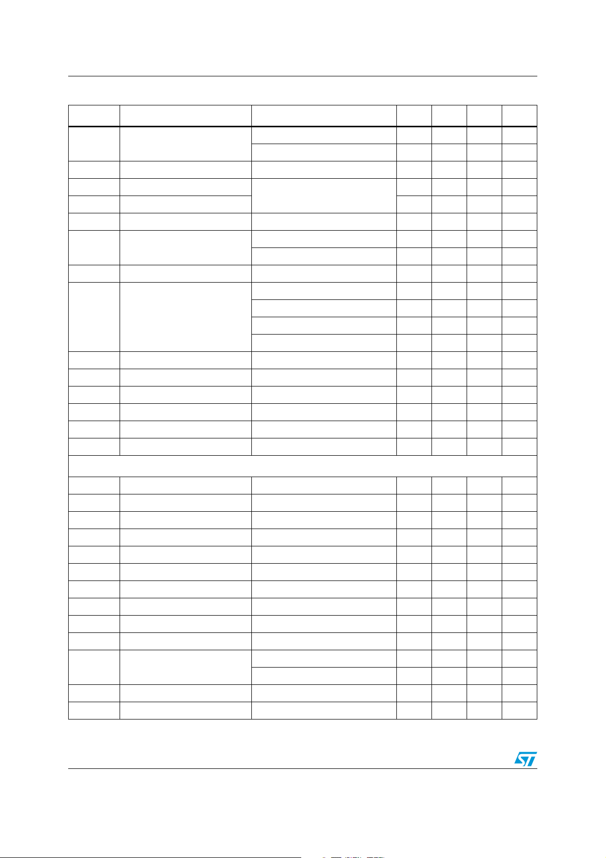
Table 2. Thermal data. . . . . . . . . . . . . . . . . . . . . . . . . . . . . . . . . . . . . . . . . . . . . . . . . . . . . . . . . . . . . 7
Table 3. Pin description . . . . . . . . . . . . . . . . . . . . . . . . . . . . . . . . . . . . . . . . . . . . . . . . . . . . . . . . . . . 8
Table 4. Supply. . . . . . . . . . . . . . . . . . . . . . . . . . . . . . . . . . . . . . . . . . . . . . . . . . . . . . . . . . . . . . . . . 11
Table 5. Absolute maximum ratings . . . . . . . . . . . . . . . . . . . . . . . . . . . . . . . . . . . . . . . . . . . . . . . . . 11
Table 6. Input section . . . . . . . . . . . . . . . . . . . . . . . . . . . . . . . . . . . . . . . . . . . . . . . . . . . . . . . . . . . . 11
Table 7. Main signal processing path . . . . . . . . . . . . . . . . . . . . . . . . . . . . . . . . . . . . . . . . . . . . . . . . 13
Table 8. Output section. . . . . . . . . . . . . . . . . . . . . . . . . . . . . . . . . . . . . . . . . . . . . . . . . . . . . . . . . . . 15
Table 9. General . . . . . . . . . . . . . . . . . . . . . . . . . . . . . . . . . . . . . . . . . . . . . . . . . . . . . . . . . . . . . . . . 16
Table 10. Bus and control inputs . . . . . . . . . . . . . . . . . . . . . . . . . . . . . . . . . . . . . . . . . . . . . . . . . . . . 17
Table 11. DC offset detector . . . . . . . . . . . . . . . . . . . . . . . . . . . . . . . . . . . . . . . . . . . . . . . . . . . . . . . . 17
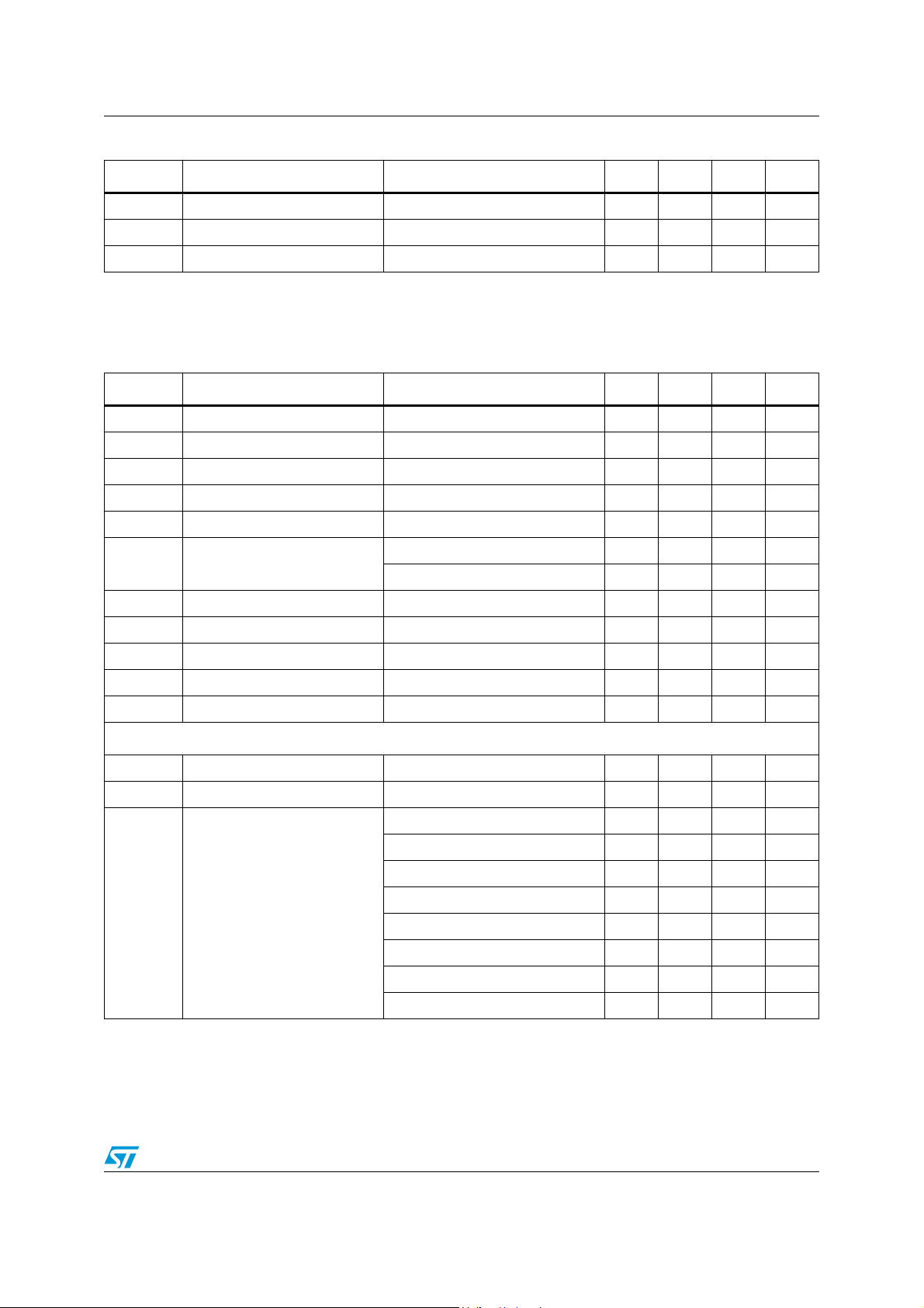
Table 12. Interface in SPI -mode . . . . . . . . . . . . . . . . . . . . . . . . . . . . . . . . . . . . . . . . . . . . . . . . . . . . 33
Table 13. Subaddress allocation (receive mode) . . . . . . . . . . . . . . . . . . . . . . . . . . . . . . . . . . . . . . . . 35
Table 14. Main signal path input (addr. 00) . . . . . . . . . . . . . . . . . . . . . . . . . . . . . . . . . . . . . . . . . . . . 36
Table 15. Main signal path, bass-filter (addr. 01) . . . . . . . . . . . . . . . . . . . . . . . . . . . . . . . . . . . . . . . . 36
Table 16. Main signal path, bass-filter (addr. 02) . . . . . . . . . . . . . . . . . . . . . . . . . . . . . . . . . . . . . . . . 37
Table 17. Main signal path, mid-filter (addr. 03) . . . . . . . . . . . . . . . . . . . . . . . . . . . . . . . . . . . . . . . . . 37
Table 18. Main signal path, treble-filter (addr. 04) . . . . . . . . . . . . . . . . . . . . . . . . . . . . . . . . . . . . . . . 38
Table 19. Main signal path, room-EQ (addr. 05) . . . . . . . . . . . . . . . . . . . . . . . . . . . . . . . . . . . . . . . . 38
Table 20. Input section, signal paths A-C (addr. 06-08) . . . . . . . . . . . . . . . . . . . . . . . . . . . . . . . . . . . 39
Table 21. Input section; other settings (addr. 09) . . . . . . . . . . . . . . . . . . . . . . . . . . . . . . . . . . . . . . . . 39
Table 22. Output section, signal path 0 (addr. 10) . . . . . . . . . . . . . . . . . . . . . . . . . . . . . . . . . . . . . . . 40
Table 23. Output section, signal path 1 and 2 (addr. 11) . . . . . . . . . . . . . . . . . . . . . . . . . . . . . . . . . . 40
Table 24. Output section, high-pass filters (addr. 12) . . . . . . . . . . . . . . . . . . . . . . . . . . . . . . . . . . . . . 41
Table 25. Output section, volume 0L, 0R, 1L, 1R, 2L, 2R (addr. 13-16, 18, 19) . . . . . . . . . . . . . . . . 42
Table 26. Output section, subwoofer low-pass filter (addr. 17) . . . . . . . . . . . . . . . . . . . . . . . . . . . . . 43
Table 27. Output section, bus-mutes (addr. 20) . . . . . . . . . . . . . . . . . . . . . . . . . . . . . . . . . . . . . . . . . 43
Table 28. DC-detector and other output section settings (addr. 21) . . . . . . . . . . . . . . . . . . . . . . . . . . 44
Table 29. Soft-mute and soft-step fader time (addr. 22) . . . . . . . . . . . . . . . . . . . . . . . . . . . . . . . . . . . 45
Table 30. Spectrum analyzer settings (addr. 23) . . . . . . . . . . . . . . . . . . . . . . . . . . . . . . . . . . . . . . . . 45
Table 31. Testing * (addr. 31) . . . . . . . . . . . . . . . . . . . . . . . . . . . . . . . . . . . . . . . . . . . . . . . . . . . . . . . 46
Table 32. Document revision history . . . . . . . . . . . . . . . . . . . . . . . . . . . . . . . . . . . . . . . . . . . . . . . . . 49
4/50 Doc ID 14100 Rev 3
Page 5

TDA7415CB List of figures
List of figures
Figure 1. Block diagram . . . . . . . . . . . . . . . . . . . . . . . . . . . . . . . . . . . . . . . . . . . . . . . . . . . . . . . . . . . . 6
Figure 2. Pin connection (top view) . . . . . . . . . . . . . . . . . . . . . . . . . . . . . . . . . . . . . . . . . . . . . . . . . . . 7
Figure 3. Signal-flow input-section (the following soft-mute and output buffer are not shown) . . . . . 18
Figure 4. Bass control range; fC= 60Hz, Q= 1.0 . . . . . . . . . . . . . . . . . . . . . . . . . . . . . . . . . . . . . . . . 19
Figure 5. Bass center frequencies; gain= 15dB, Q= 1.0 . . . . . . . . . . . . . . . . . . . . . . . . . . . . . . . . . . 20
Figure 6. Bass filter quality factors; f
Figure 7. Bass DC-mode frequency responses; gain= 15dB, Q= 1.5 . . . . . . . . . . . . . . . . . . . . . . . . 21
Figure 8. Mid control range; fC= 1kHz, Q= 1.0 . . . . . . . . . . . . . . . . . . . . . . . . . . . . . . . . . . . . . . . . . 21
Figure 9. Mid center frequencies; gain= 15dB, Q= 1.0 . . . . . . . . . . . . . . . . . . . . . . . . . . . . . . . . . . . 22
Figure 10. Mid filter quality factors; fC= 1kHz, gain= 15dB . . . . . . . . . . . . . . . . . . . . . . . . . . . . . . . . . 22
Figure 11. Treble control range; fC= 12.5kHz, Q= 1.0 . . . . . . . . . . . . . . . . . . . . . . . . . . . . . . . . . . . . . 23
Figure 12. Treble center frequencies; gain= 15dB, Q= 1.0 . . . . . . . . . . . . . . . . . . . . . . . . . . . . . . . . . 23
Figure 13. Room-EQ control range; fC= 200Hz, Q= 1.0 . . . . . . . . . . . . . . . . . . . . . . . . . . . . . . . . . . . 24
Figure 14. Room-EQ notch frequencies; attenuation= -7dB, Q= 1.0. . . . . . . . . . . . . . . . . . . . . . . . . . 24
Figure 15. Room-EQ notch filter quality factors; fC= 200Hz, attenuation= 7dB.. . . . . . . . . . . . . . . . . 25
Figure 16. Signal flow output section . . . . . . . . . . . . . . . . . . . . . . . . . . . . . . . . . . . . . . . . . . . . . . . . . . 26
Figure 17. High-pass corner frequencies; Q= 0.707 . . . . . . . . . . . . . . . . . . . . . . . . . . . . . . . . . . . . . . 27
Figure 18. Low-pass corner frequencies; Q= 0.707. . . . . . . . . . . . . . . . . . . . . . . . . . . . . . . . . . . . . . . 27
Figure 19. Line-driver output with reference generation scheme. . . . . . . . . . . . . . . . . . . . . . . . . . . . . 28
Figure 20. Soft-mute signal envelope versus time . . . . . . . . . . . . . . . . . . . . . . . . . . . . . . . . . . . . . . . . 29
Figure 21. Spectrum analyzer block diagram . . . . . . . . . . . . . . . . . . . . . . . . . . . . . . . . . . . . . . . . . . . 30
Figure 22. Read cycle timing diagram . . . . . . . . . . . . . . . . . . . . . . . . . . . . . . . . . . . . . . . . . . . . . . . . . 30
Figure 23. DC-offset detection circuit (simplified) . . . . . . . . . . . . . . . . . . . . . . . . . . . . . . . . . . . . . . . . 31
Figure 24. Switching characteristics (SPI-mode): . . . . . . . . . . . . . . . . . . . . . . . . . . . . . . . . . . . . . . . . 32
Figure 25. Interface in SPI -mode diagram . . . . . . . . . . . . . . . . . . . . . . . . . . . . . . . . . . . . . . . . . . . . . 32
Figure 26. I
Figure 27. Typical application connections diagram . . . . . . . . . . . . . . . . . . . . . . . . . . . . . . . . . . . . . . 47
Figure 28. LQFP64 mechanical data and package dimensions . . . . . . . . . . . . . . . . . . . . . . . . . . . . . 48
2
C bus interface diagram . . . . . . . . . . . . . . . . . . . . . . . . . . . . . . . . . . . . . . . . . . . . . . . . . . 33
= 60Hz, gain= 15dB. . . . . . . . . . . . . . . . . . . . . . . . . . . . . . . . . 20
C
Doc ID 14100 Rev 3 5/50
Page 6
Block diagram TDA7415CB
1 Block diagram
Figure 1. Block diagram
6/50 Doc ID 14100 Rev 3
Page 7

TDA7415CB Pin description
2 Pin description
2.1 ESD:
All pins are protected against ESD according to the MIL883 standard.
2.2 Thermal data
Table 2. Thermal data
Symbol Description Value Unit
R
th j-pins
Thermal resistance junction-to-pins 50 °C/W
2.3 Pin assignment
Figure 2. Pin connection (top view)
Doc ID 14100 Rev 3 7/50
Page 8
Pin description TDA7415CB
2.4 Pin function
Table 3. Pin description
PIN
Direction
(1)
Name Description
1 I CDCh L CD-changer input, pseudo differential, left channel
2 I CDCh Common CD-changer input, pseudo differential common
3 I CDCh R CD-changer input, pseudo differential, right channel
4 I AUX L Aux./Navigation input, pseudo differential, left channel
5 I AUX Common Aux./Navigation input, pseudo differential common
6 I AUX R Aux./Navigation input, pseudo differential, right channel
7 O MUXA L IN-Section, signal path A output (Main), left channel
8 O MUXA R IN-Section, signal path A output (Main), right channel
9 O MUXB L IN-Section, signal path B output (Sub), left channel
10 O MUXB R IN-Section, signal path B output (Sub), right channel
11 O MUXC L IN-Section, signal path C output (Aux.), left channel
12 O MUXC R IN-Section, signal path C output (Aux.), right channel
13 I WinIn Zero-window Sense input (from power-amp)
14 P WinTC0 Zero-window comparator 0 time constant
15 P WinTC1 Zero-window comparator 1 time constant
16 O DCErr DC-detector Error output
17 I SEL Interface-select; SPI: receive enable
2
18 I / OC SDA I
19 I SCL I
C/SPI-bus serial data input/output
2
C/SPI-bus serial clock input
20 I SAclk Spectrum analyzer clock input
21 I SAres. Spectrum analyzer reset
22 O SAout Spectrum analyzer analog voltage output
23 I SAin Spectrum analyzer external input
24 P Ref5V5
5.5V-reference decoupling pin, connects to external
capacitor
25 I VolIn L Main signal path input, left channel
26 I VolIn R Main signal path input, right channel
27 P Ref3V3
3.3V-reference decoupling pin, connects to external
capacitor
28 I Mute0 OUT-section, signal path 0 (front) direct mute
29 I Mute1 OUT-section, signal path 1 (rear) direct mute
30 I Mute2 OUT-section, signal path 2 (other) direct mute
31 O ACout L Main signal path output, left channel
8/50 Doc ID 14100 Rev 3
Page 9
TDA7415CB Pin description
Table 3. Pin description (continued)
PIN
Direction
(1)
Name Description
32 O ACout R Main signal path output, right channel
33 I ACin3 R OUT-section, AC-coupled input 3, right channel
34 I ACin3 L OUT-section, AC-coupled input 3, left channel
35 I ACin2 R OUT-section, AC-coupled input 2, right channel
36 I ACin2 L OUT-section, AC-coupled input 2, left channel
37 I ACin1 R OUT-section, AC-coupled input 1, right channel
38 I ACin1 L OUT-section, AC-coupled input 1, left channel
39 I ACin0 R OUT-section, AC-coupled input 0, right channel
40 I ACin0 L OUT-section, AC-coupled input 0, left channel
41 S VCC Device supply pin
42 S GND Device ground pin
43 O LDout2 R Line-driver output, signal path 2 (other), right channel
44 O LDout2 L Line-driver output, signal path 2 (other), left channel
45 O LDout1 R Line-driver output, signal path 1 (rear), right channel
46 O LDout1 L Line-driver output, signal path 1 (rear), left channel
47 S PGND
48 P PREF
Device ground pin (dual supply), connects to system ground
Line-driver-reference decoupling pin, connects to external
capacitor
49 O LDout0 R Line-driver output, signal path 0 (front), right channel
50 O LDout0 L Line-driver output, signal path 0 (front), left channel
51 S VP Device supply pin (dual supply), Output section
52 O PAout1 R Out-section rear output, right channel
53 O PAout1 L Out-section rear output, left channel
54 O PAout0 R Out-section front output, right channel
55 O PAout0 L Out-section front output, left channel
56 I Mute C IN-section, signal path 2 (Aux.) direct mute
57 I Mute B IN-section, signal path 1 (Sub) direct mute
58 I Mute A IN-section, signal path 0 (Main) direct mute
59 I Tuner L Tuner input, left channel
60 I Tuner R Tuner input, right channel
61 I CD L CD input, left channel
62 I CD R CD input, right channel
63 I MD L Minidisk (mono-differential Phone+) input, left channel
64 I MD R Minidisk (mono-differential Phone-) input, right channel
1. I= input, O= output, OC =open collector, P= passive external component, S= supply
Doc ID 14100 Rev 3 9/50
Page 10

Deatailed features TDA7415CB
3 Deatailed features
The TDA7415CB is composed of four major building blocks. - The IN-section, the spectrumanalyzer, the main signal processing path and the OUT-section; Individually featuring:
IN section
● Three independent signal-paths (front, rear and auxiliary) with independent soft-mute.
● Six stereo inputs; 3 single ended; 1 single ended or full differential mono; 2 quasi-
differential.
● ±15dB level-adjust with 1 dB steps.
● Pin-accessible and/or I
Spectrum analyzer
● 7-band, fully integrated 2
different visual behavior.
● Dedicated one or two-wire serial port for analog data-readout.
● Analog output voltage 3.3 V-μP compatible.
Main signal processing path
2
C/SPI-controlled soft-mute (direct mute) for each signal path.
nd
-order band-pass filters with programmable filter quality for
● ±15dB level-adjust with 1dB steps.
● Fully integrated bass-, middle- and treble-tone control. All filters offer 2
nd
-order
frequency response with programmable filter quality and center frequency.
● Room-acoustics notch filter (Room-EQ) allows the suppression of primary car-body
resonance.
OUT section
● Three independent signal-paths (front, rear and others) with individual soft-mute.
● Four AC-coupled, single ended stereo inputs.
● Pin-accessible soft-mute (direct mute), for each signal path.
2
● I
C/SPI-controlled soft-mute, independent for all six (mono) channels
● Main signal path monitor-select (pre/post tone control).
● L/R-channel independent phone, navigation or phone/navigation-mix signal interrupts
for front signal path; L/R-channel independent phone or navigation interrupts for rearand others-path.
nd
● 2
● 2
● Soft-step volume with 79 to 25 dB range for each signal path.
● Four dedicated outputs for an internal (on-board) power amplifier.
● Six 4V
● Offset voltage detection circuit for on-board power amplifier failure diagnosis.
-order frequency response high-pass filters for front- and rear-signal path.
nd
-order frequency response subwoofer low-pass filter for others-signal path.
line-driver outputs for an external (remote) power amplifier.
RMS
10/50 Doc ID 14100 Rev 3
Page 11
TDA7415CB Electrical specification
4 Electrical specification
4.1 Supply
Table 4. Supply
Symbol Parameter Test conditions Min. Typ. Max. Unit
V
V
I
total
Supply voltage - 7.5 8.5 9.5 V
CC
Supply current (line
P
driver)
- 7.5 12 13 V
Total supply current VCC = 8.5 V; VP = 12V - 45 - mA
SVRR Ripple rejection @ 1 kHz Audio processor (all filters flat) - 60 - dB
4.2 Absolute maximum ratings
Table 5. Absolute maximum ratings
Symbol Parameter Value Unit
V
T
T
V
amb
Operating supply voltage 10 V
CC
Operating supply voltage 13 V
P
Operating temperature range -40 to 85 °C
Storage temperature range -55 to +150 °C
stg
4.3 Electrical characteristcs
4.3.1 Input section
V
= 8.0 V; VP = 12.0 V; T
CC
otherwise specified.
Table 6. Input section
Symbol Parameter Test conditions / remark Min. Typ. Max. Unit
R
in
V
CL
CMRR
Input Impedance
Input Clipping Level
(THD ≤ 0.1%)
Common mode rejection ratio
Differential inputs (CD, AUX.)
= 25 °C; RL =10 kΩ ; all gains = 0 dB; f = 1 kHz; unless
amb
Single-ended inputs 70 100 130 kΩ
Differential inputs 70 100 130 kΩ
MD-input, differential mode 35 56 65 kΩ
Single ended inputs 1.4 1.5 - V
Differential inputs;
VCM = 1 V
V
CM
= 1 V
RMS
RMS
(1)
2.0 2.2 - V
@ 1 kHz 40 70 - dB
@ 10 kHz 40 60 - dB
Doc ID 14100 Rev 3 11/50
RMS
RMS
Page 12
Electrical specification TDA7415CB
Table 6. Input section (continued)
Symbol Parameter Test conditions / remark Min. Typ. Max. Unit
V
CMRR
S
IN
G
IN MIN
G
IN MAX
G
STEP
V
DC
AT T
MUTE
Common mode rejection ratio
MD
Mono differential input (MD)
= 1 V
CM
V
= 1 V
CM
Input separation - 80 100 - dB
Min. input gain
input to output,
Max. input gain 14 15 16 dB
Gain-adjust step resolution - 0.5 1 1.5 dB
Adjacent gain steps - 0.5 6 mV
DC-offset steps
G
to G
MIN
Mute attenuation - 80 100 - dB
T1 0.10.240.4 ms
@ 1 kHz 40 66 - dB
RMS
@ 10 kHz 40 56 - dB
RMS
(1)
MAX
-16 -15 -14 dB
-535mV
t
SMC
Soft-mute completion time,
ramp-up or -down
T2 0.25 0.48 0.75 ms
T3 7 10.2 13 ms
T4 16 20.4 26 ms
V
NO
V
OUT,max
Output-noise, MUX-Outputs 20 Hz - 20 kHz; all flat, 0 dB - 8 15 µV
Maximum output level R
≥ 2 kΩ; THD ≤ 0.1 % 1.4 1.5 - V
LOAD
RL Output load resistance THD ≤ 0.1 % 1.0 - - kΩ
Output load capacitance - - - 10 nF
L
Output impedance - - 24 100 Ω
DC voltage level - 3.1 3.3 3.5 V
R
C
OUT
V
DC
Spectrum Analyzer (see figure 21)
V
V
f
SAclk
t
SAdel
R
SAin
SAout
f
C1
f
C2
f
C3
f
C4
f
C5
f
C6
f
C7
Q
Input impedance - 70 100 130 kΩ
in
Max. Input level, SAin-pin 3.3V full scale at SAout-pin - 1.0 - V
Output Voltage Range R
Center Frequency, band 1
Center Frequency, band 2
Center Frequency, band 3
Center Frequency, band 4
Center Frequency, band 5
Center Frequency, band 6
Center Frequency, band 7
Filter Quality Factor
f
(2)
(2)
(2)
(2)
(2)
(2)
(2)
(2)
LOAD
≥ 1MΩ; V
SAin
≤ 1V
RMS
0-3.3V
-556269Hz
- 141 157 173 Hz
- 356 396 436 Hz
- 0.911.1kHz
- 2.26 2.51 2.76 kHz
- 5.70 6.34 6.98 kHz
- 14.4 16.0 17.6 kHz
Q
1
Q
2
1.40 1.75 2.10 -
2.80 3.5 4.20 -
Read-out clock frequency - 1 - 100 kHz
Analog output delay time C
at SAout-pin ≤ 100 pF - 1 2 μs
Load
RMS
RMS
12/50 Doc ID 14100 Rev 3
Page 13
TDA7415CB Electrical specification
Table 6. Input section (continued)
Symbol Parameter Test conditions / remark Min. Typ. Max. Unit
t
repeat
t
intres
t
SAres
1. All differential inputs or differential configurations have -3 dB input gain.
Read-out cycle repeat time Recommended refresh rate 50 - - ms
Internal reset time Auto-reset mode enabled 3 4 5 ms
Reset pulse width Auto-reset mode disabled 500 - - ns
4.3.2 Main signal processing path
Table 7. Main signal processing path
Symbol Parameter Test conditions / remark Min. Typ. Max. Unit
R
in
V
CL
G
IN MIN
G
IN MAX
G
STEP
V
DC
V
OUT,max
R
L
C
OUT
R
OUT
V
DC
Bass Control
Input impedance - 35 50 65 kΩ
Input clipping level THD ≤ 0.1 % 1.4 1.5 - V
Min. input gain input to output; all filters flat -16 -15 -14 dB
Max. input gain - 14 +15 16 dB
Gain-adjust step resolution - - 1 - dB
Adjacent gain steps - 0.5 6 mV
DC-offset steps
G
Maximum output level R
to G
MIN
LOAD
MAX
≥ 2 kΩ; THD ≤ 0.1 % 1.4 1.5 - V
-530mV
Output load resistance THD ≤ 0.1 % 1.0 - - kΩ
Output load capacitance - - - 10 nF
Output impedance - - 24 36 Ω
DC voltage level - 3.1 3.3 3.5 V
RMS
RMS
G
RANGE
A
STEP
Gain control range - ±13 ±15 ±17 dB
Step resolution - 0.5 1 1.5 dB
f
C0
f
C1
f
C2
f
f
Center frequency
C
(1)
C3
f
C4
f
C5
f
C6
f
C7
30 40 50 Hz
40 50 50 Hz
50 60 70 Hz
60 70 90 Hz
60 80 100 Hz
80 100 120 Hz
100 120 140 Hz
120 150 170 Hz
Doc ID 14100 Rev 3 13/50
Page 14
Electrical specification TDA7415CB
Table 7. Main signal processing path (continued)
Symbol Parameter Test conditions / remark Min. Typ. Max. Unit
Q
DC
BASS
GAIN
Quality factor
Bass DC-gain
(1)
MID control
G
RANGE
A
STEP
Q
f
MID
Gain control range - ±13 ±15 ±17 dB
Step resolution - 0.5 1 1.5 dB
Center frequency
C
Quality factor
(2)
(2)
Treble Control
G
RANGE
A
STEP
f
Gain control range - ±13 ±15 ±17 dB
Step resolution - 0.5 1 1.5 dB
Center frequency
C
(1))
ROOM-EQ (acoustics notch-filter)
Q
1
Q
2
Q
3
Q
4
0.911.1 -
1.13 1.25 1.38 -
1.35 1.5 1.65 -
1.822.2 -
DC-mode= off -1 0 1 dB
DC-mode= on 3.5 4.4 5.5 dB
f
C1
f
C2
f
C3
f
C4
Q
1
Q
2
f
C1
f
C2
f
C3
f
C4
450 500 550 Hz
0.911.1kHz
1.35 1.5 1.65 kHz
1.822.2kHz
0.511.1 -
1.822.2 -
6.4 10 13.6 kHz
8.0 12.5 17 kHz
9.6 15 20.4 kHz
11.2 17.5 23.8 kHz
G
RANGE
A
STEP
f
Q
1. Min and Max values are calculated according to simulation results; Functionality is guaranteed by measuring a directly
correlated parameter
Gain control range - -0…9- dB
Step resolution Non-uniform, see description 1 - 2 dB
Notch frequency
C
Quality factor
EQ
(1)
(1)
f
N1
f
N2
f
N3
f
N4
Q
1
Q
2
162 180 198 Hz
180 200 220 kHz
198 220 242 kHz
216 240 264 kHz
0.911.1 -
1.822.2 -
14/50 Doc ID 14100 Rev 3
Page 15
TDA7415CB Electrical specification
4.3.3 Output section
V
= 8.0 V; VP = 12.0 V; T
CC
otherwise specified
Table 8. Output section
Symbol Parameter Test conditions Min. Typ. Max. Unit
R
in
V
CL
AT T
MUTE
t
SMC
Volume (Soft-step)
G
MAX
A
MAX
A
STEP
E
A
E
T
V
DC
High Pass
f
C
Q
HP
Subwoofer low pass
Input impedance AC0…3 inputs 35 50 65 kΩ
Input Clipping Level THD ≤ 0.1% 1.4 1.5 - V
Mute Attenuation - 80 100 - dB
Soft-mute completion time,
ramp-up or -down
Max. gain - - 25 - dB
Max. attenuation - -82 -79 -76 dB
Step resolution - 0.5 1 1.5 dB
Attenuation set error
Tracking error - - - 2 dB
DC steps
Center frequency
Quality factor
(1)
(2)
= 25 °C; RL =10 kΩ ; all gains = 0 dB; f = 1 kHz; unless
amb
RMS
T1 0.21 0.24 0.26 ms
T2 0.43 0.48 0.52 ms
T3 10.47 11.5 12.45 ms
T4 5.23 5.76 6.22 ms
G= -20 to +20 dB -1.25 0 +1.25 dB
G= -20 to -60 dB -3 0 3 dB
Adjacent attenuation steps - 0.1 3 mV
From 0dB to G
f
C0
f
C1
f
C2
f
C3
f
C4
f
C5
f
C6
f
C7
MIN
-0.55mV
34 40 46 Hz
52 60 68 Hz
72 80 88 Hz
90 100 110 Hz
108 120 132 Hz
135 150 165 Hz
162 180 198 Hz
198 220 242 Hz
Butterworth characteristics 0.665 0.707 0.750 -
f
Q
Center Frequency
C
Quality Factor
HP
Audio outputs
V
PA ,m a x
Max. output level; PA-outputs R
(2)
(2)
f
C0
f
C1
f
C2
f
C3
f
C4
44 50 56 Hz
54 60 66 Hz
72 80 88 Hz
90 100 110 Hz
108 120 132 Hz
Butterworth characteristics 0.665 0.707 0.750 -
≥ 2 kΩ; THD ≤ 0.1 % 1.88 2 - V
LOAD
Doc ID 14100 Rev 3 15/50
RMS
Page 16

Electrical specification TDA7415CB
Table 8. Output section (continued)
Symbol Parameter Test conditions Min. Typ. Max. Unit
V
LD,max
R
C
R
L
L
OUT
Max. output level; LD-outputs
as above; V
as above; VP = 12 V 3.75 4 V
Output load resistance THD ≤ 0.1 %; all outputs 1.0 kΩ
Output load capacitance All outputs 10 nF
Output impedance All outputs 24 100 Ω
= 8.0 V 2.20 2.75 V
CC
RMS
RMS
PA-outputs 3.8 4.0 4.2 V
V
1. All differential inputs or differential configurations have -3dB input gain.
2. Min and Max values are calculated according to simulation results; Functionality is guaranteed by measuring a directly
correlated parameter
DC voltage level
DC
LD-outputs
VP / 2
-200mV
/ 2
V
/ 2
V
P
P
+200mV
V
4.3.4 General
Table 9. General
Symbol Parameter Test conditions / remark Min. Typ. Max. Unit
BW = 20 Hz to
V
NO
Output noise
20 kHz
output
mode
-1015μV
unveighted all flat, 0 dB - 12 20 μV
S/N Signal to noise ratio
d Distortion
Channel separation L/R - 80 100 - dB
C
Total tracking error
T
Internal POR Voltage - - - 3.4 V
V
S
E
POR
all flat, 0 dB; V
= 1.5 V
O
RMS
All tone filters +10 dB;
A-weighted; V
V
= 1 V
OUT
= 1.5 V
O
; all stages 0 dB - 0.01 0.1 %
RMS
RMS
All tone filters +10 dB;
A-weighted; V
= 0 to -20 dB - 0 1 dB
A
V
= -20 to -60 dB - 0 2 dB
A
V
= 1.5 V
O
RMS
-110-dB
-84-dB
- 0.05 0.1 %
16/50 Doc ID 14100 Rev 3
Page 17

TDA7415CB Electrical specification
4.3.5 Bus and control inputs
Table 10. Bus and control inputs
2
(I
C/SPI, spectrum analyzer, direct-mute, offset detector)
Symbol Parameter Test conditions / remark Min. Typ. Max. Unit
V
V
V
TH
V
TH
I
IN
V
TH,SPI
V
O,ACK
R
PULLUP
I
PULLUP
Input low voltage SDA-, SCL-, SEL-, WinIn-pin - 0.8 0.7 V
IL
Input high voltage - 2.5 2.4 - V
IH
Input threshold voltage SAres-, SAclk-, all Mute-pins - 1.5 - V
Input threshold hysteresis - - 100 - mV
Input current VIN= 0.4V; SDA-, SCL-pin -5 - 5 μA
SPI-mode threshold
voltage
SDA-acknowledge output
volt.
(1)
= 1.6mA - - 0.4 V
I
O
--5.5V
Pull-up resistance WinIn-pin 30 50 70 kΩ
Pull-up current VIN= 0V, all Mute-pins 50 100 150 μA
SPI-mode - - 2000 kbit/s
f
SCKmax
1. pull-up is needed for I2C Mute
Maximum clock speed
I2C-mode - - 800 kbit/s
4.3.6 DC offset detector
Table 11. DC offset detector
Symbol Parameter Test conditions / remark Min. Typ. Max. Unit
V
τ
sp
I
Err,charge
I
Err,discharge
V
OutH
V
OutL
V1 - ±25 - mV
V2 - ±50 - mV
th
Zero comp. window size
V3 - ±75 - mV
V4 - ±100 - mV
τ1-7.5-μs
Max. rejected spike
length
τ2-15-μs
τ3-22.5-μs
τ4-30-μs
DCErr charge current - 1 5 10 μA
DCErr discharge current - 2.5 5 7.5 mA
DCErr high voltage - 2.5 3.3 - V
DCErr low voltage - - 150 300 mV
Doc ID 14100 Rev 3 17/50
Page 18

Description of the audio processor TDA7415CB
5 Description of the audio processor
As can be seen from the block diagram in Figure 1, the Audio processor is composed of
three building blocks. - The INPUT-Section, the MAIN-SIGNAL-PROCESSING-path and the
OUTPUT-Section.
This chapter will give more insight into the different blocks and describe their function.
5.1 Input section
The Input-Section of the TDA7415CB incorporates three independent stereo signal paths,
where each can connect to a variety of inputs and the AC3 input from the Output-section for
monitoring purposes. For simplicity only the left inputs are shown.
After selection by the Main-, Sub-, and/or Auxiliary-source selector, the signal passes a
gain-adjust amplifier, a soft-mute stage and finally a buffer before it is output at the device
output-pins. The soft-mute circuit will be described later.
Figure 3. Signal-flow input-section (the following soft-mute and output buffer are
not shown)
18/50 Doc ID 14100 Rev 3
Page 19

TDA7415CB Description of the audio processor
The CD-Changer- and Auxiliary/Navigation-inputs are quasi-differential inputs, where the
'out-of-phase' or ground signals of both channels share one common input. The Minidiskinput (MD) may be reconfigured for a true mono differential input as required by many phone
units. Please note that all differential inputs dampen the signal by 3dB.
Additionally, each differential input-pin features a 'fast charge'-switch (*) allowing quickly
charging external, large coupling capacitors upon power-on of the device. For normal
operation, these switches need to be released by programming the corresponding bit.
For programming of the Input-section, see the programming chapter
5.2 Main signal processing path
The main-signal-processing path incorporates a classical three-band tone control (bass, mid
and treble) that is preceded by a gain-adjust amplifier and completed by a dedicated room
acoustics notch-filter (Room-EQ, see figure 1) that allows defeating the main car-body
resonance.
Hereafter, the filters composing the tone control and room-EQ will be presented.
5.2.1 Bass filter
There are four parameters programmable in the bass-filter stage.
1. Control range: Figure 4 shows the control range in the frequency domain at 60Hz
center frequency.
Figure 4. Bass control range; f
= 60Hz, Q= 1.0
C
Doc ID 14100 Rev 3 19/50
Page 20

Description of the audio processor TDA7415CB
2. Center frequency: Figure 5 shows all the selectable center frequencies at a gain of
15dB
Figure 5. Bass center frequencies; gain= 15dB, Q= 1.0
3. Quality factor: Figure 6 shows the four selectable filter quality factors at a gain of 15dB
Figure 6. Bass filter quality factors; f
= 60Hz, gain= 15dB.
C
20/50 Doc ID 14100 Rev 3
Page 21

TDA7415CB Description of the audio processor
4. DC-mode: Figure 7 shows the effect of the DC-mode at a filter gain of 15dB. In this
mode the DC-gain is increased by 4.4dB. In addition the programmed center
frequencies and quality factors are decreased by 25%, which realizes alternative
frequency responses.
Figure 7. Bass DC-mode frequency responses; gain= 15dB, Q= 1.5
5.2.2 Mid filter
There are three parameters programmable in the mid-filter stage.
1. Control Range: Figure 8 shows the control range in the frequency domain at 1kHz
center frequency.
Figure 8. Mid control range; f
= 1kHz, Q= 1.0
C
Doc ID 14100 Rev 3 21/50
Page 22

Description of the audio processor TDA7415CB
2. Center frequency: Figure 9 shows the four selectable center frequencies at a gain of
15dB.
Figure 9. Mid center frequencies; gain= 15dB, Q= 1.0
3. Quality Factor: Figure 10 shows the two selectable filter quality factors at a gain of
15dB.
Figure 10. Mid filter quality factors; f
= 1kHz, gain= 15dB
C
22/50 Doc ID 14100 Rev 3
Page 23

TDA7415CB Description of the audio processor
5.2.3 Treble filter
There are two parameters programmable in the treble-filter stage.
1. Control Range: Figure 11 shows the control range in the frequency domain at 12.5kHz
center frequency.
Figure 11. Treble control range; f
= 12.5kHz, Q= 1.0
C
2. Center frequency: Figure 12 shows the four selectable center frequencies at a gain of
15dB
Figure 12. Treble center frequencies; gain= 15dB, Q= 1.0
Doc ID 14100 Rev 3 23/50
Page 24

Description of the audio processor TDA7415CB
5.2.4 Room EQ filter
There are three parameters programmable in the room-EQ stage.
1. Control range: Figure 13 shows the control range in the frequency domain at 200Hz
center frequency. The filter has intentional non-uniform attenuation steps. These are
1dB, 2dB, 3dB, 4dB, 5.5dB, 7dB and 9dB.
Figure 13. Room-EQ control range; f
= 200Hz, Q= 1.0
C
2. Notch frequency: Figure 14 shows the four selectable notch frequencies at a gain of
15dB
Figure 14. Room-EQ notch frequencies; attenuation= -7dB, Q= 1.0.
24/50 Doc ID 14100 Rev 3
Page 25

TDA7415CB Description of the audio processor
3. Quality factor: Figure 15 shows the two selectable filter quality factors at a gain of
15dB
Figure 15. Room-EQ notch filter quality factors; f
= 200Hz, attenuation= 7dB.
C
Doc ID 14100 Rev 3 25/50
Page 26

Description of the audio processor TDA7415CB
5.3 Output path
As the Input-Section, the Output-Section of the TDA7415CB incorporates also three
independent stereo signal paths, where each can connect to two out of four AC-coupled,
single-ended inputs and to some dedicated signals originating from the input-section and/or
main-signal-path. For simplicity only one channel is shown in Figure 16. Interruption
switches follow the input selectors that can quickly toggle to the phone-, navigation-, or
phone/navigation-mix signal independently for each signal path and single L/R-channel. The
pre-selection of the interrupt source is common for all signal paths.
Figure 16. Signal flow output section
Signal path 0 and 1 (front and rear) may optionally enter high-pass filters whereas signal
path 2 (other) can be low-pass filtered for subwoofer applications. Anti-radiation filters are
integrated for all signal paths but there are no anti-alias filters present at the inputs, since for
most signal sources it is unlikely to introduce significant high frequency energy. However, if
present, the system designer must take care to filter out high frequency components by
means of an external RC-low-pass filter located at the AC-input pins. Soft-mute stages and
a soft-step volume, that offer fast and click-less muting and/or volume changing follow all
three filters. The soft mute circuit will be described later.
Five stereo pairs of output buffers finally complete the Output-section: Signal-path 2
exclusively feeds a line driver output that is capable of 4V
external (remote) power amplifiers. The other signal-paths 1 & 2 feature both, a line driver
output and a dedicated internal (on board) power amplifier output with 3dB fixed gain. To
maximize the line-driver output swing, when the dual-supply option (V
26/50 Doc ID 14100 Rev 3
output level as required by
RMS
= 9V, VP = 12V) is
CC
Page 27

TDA7415CB Description of the audio processor
not needed or available, the line-driver output stages may be programmed for lower gain,
still delivering 2.75V
For programming of the Output-section, see the programming chapter
Hereafter, the different circuits composing the Output-section will be presented.
RMS
.
5.3.1 High pass filter
1. Corner frequency: Figure 17 shows all the selectable corner frequencies for the highpass filter
Figure 17. High-pass corner frequencies; Q= 0.707
5.3.2 Low pass (subwoofer) filter
1. Corner frequency: Figure 18 shows all the selectable corner frequencies for the lowpass filter.
Figure 18. Low-pass corner frequencies; Q= 0.707
Doc ID 14100 Rev 3 27/50
Page 28

Description of the audio processor TDA7415CB
Remark: Both filters offer a 'Butterworth' roll-off response
5.3.3 Line driver output stage (presenting the reference concept)
In order to adapt to two different supply-voltages for the dual-supply option, while
maintaining the highest possible output swing when only a single supply is available, the
line-driver output was realized as differential amplifier biased around the two device
references PREF and Vref3V3 (see Figure 19). The output DC-voltage precisely tracks the
DC-voltage present at the PREF-pin that is half the VP-supply. However, forcing the PREF
pin to any desired value could alter this DC-voltage, neglected the remaining output swing.
Figure 19. Line-driver output with reference generation scheme
In a dual-supply application (V
= 8.5V, VP = 12V) the output gain should be set to 9dB to
CC
obtain a 4VRMS output level. For a single-supply application (V
an output level of 2.75V
obtainable. Consequently, to avoid clipping in the output stages
RMS
the gain needs to be reduced to 5.5dB. For the programming of the output gain, see the
programming chapter.
Proper power sequencing is no critical issue for the TDA7415. However, it is recommended
that both supply-voltages should follow each other within one diode forward-drop (<1V)
before reaching their final value.
5.3.4 Soft mute
As can be seen from the block-diagram in figure 1, there are 6 soft-mute circuits placed
inside the TDA7415CB: Three each, in both the Input-section and the Output-section that
serve the independent signal-paths. A soft-mute can either be achieved by pulling one of the
28/50 Doc ID 14100 Rev 3
=VP = 8.5V) there is still
CC
Page 29

TDA7415CB Description of the audio processor
six soft-mute pins low (hardware-mute) or by assessing the corresponding programming bits
(software-mute).
For the In-section, a soft-mute is always stereo for each of the three signal-paths and the
bus-triggered mute exactly corresponds to the pin-triggered mute, with the exception that
the later is inherently faster in response. This behavior is also true for the Out-section, but
here the bus-triggered mute is independent for all six single L/R-channels.
All mute-pins have internal pull-ups connected to a 3,3Volts reference that allow the
connection to either a 3,3V- or a 5V-microproccessor. Reverse flowing currents are limited to
100µA, so that the mute-pins may be driven by both, open-drain or push-pull outputs.
The envelope slope of the soft-mute was realized in a special S-shaped curve to soften the
mute transitions in the critical regions (see Figure 20). The completion time for full mute / no
mute is programmable by I
Figure 20. Soft-mute signal envelope versus time
2
C/SPI-bus in four different values.
Note: A triggered mute is always completed and cannot be interrupted by a change of the initial
mute condition.
For the programming of the soft-mute, see the programming chapter.
5.4 Spectrum analyzer
A fully integrated seven-band spectrum analyzer is present in the TDA7415CB (Figure 21).
The spectrum analyzer consists of seven band pass filters followed by rectifiers with sample
capacitors that store the maximum peak signal level for each band since the last read cycle.
This peak signal level can be read by a microprocessor at the SAout-pin. To allow easy
interfacing to an analog input-port of a microprocessor, the output voltage at this pin is
referred to device ground. Since the output voltage follows the peak level linearly, the
microprocessor should take care for a logarithmic conversion (e.g. logarithmic look-up
table).
Doc ID 14100 Rev 3 29/50
Page 30

Description of the audio processor TDA7415CB
The spectrum analyzer's input signal is either the mono-sum of the stereo MUXA-output or
alternatively a signal input at the SAin-pin. In order to have some influence on the visual
behavior in a given application the filter quality for all band-pass filters may be programmed
for two different qualities, with the higher filter quality creating a faster, more differentiating
optical response. If the spectrum analyzer is disabled both, the SAres- and the SAclk-pin
should be tied to ground.
Figure 21. Spectrum analyzer block diagram
The microprocessor starts a read cycle with a negative going clock edge at the SAclk input.
On the following positive clock edges, the stored peak signal level of the band pass filters is
subsequently switched to SAout. Each analog output value is valid after the time t
SAdel
. A
reset of the sample capacitors is triggered by either pulling the SAres-pin low any time or by
setting-up the spectrum-analyzer for Auto-reset mode. Although not shown in Figure 22, for
the Auto-reset mode a reset is generated whenever SAclk remains high for the time t
intres
.
Note that a proper auto-reset requires the clock signal SAclk to be held at high potential and
that the reset is not repetitive. Once a reset was triggered, a new read-out cycle should not
be initiated before the time t
has passed. This allows sufficient settling of the filters.
repeat
Figure 22 illustrates the read cycle timing of the spectrum analyzer.
Figure 22. Read cycle timing diagram
30/50 Doc ID 14100 Rev 3
Page 31

TDA7415CB Description of the audio processor
5.5 DC offset detector
Using the DC offset detection circuit (figure 22) an offset voltage difference between the
audio power amplifier and theTDA7415CB's PA-outputs can be detected, preventing serious
damage to the loudspeakers. The circuit compares whether the signal crosses the zero level
inside the audio power at the same time as in the speaker cell. The output of the zerowindow-comparator of the power amplifier must be connected with the WinIn-input of the
TDA7415CB. The WinIn-input has an internal pull-up resistor connected to 5,5Volts. It is
recommended to drive this pin with open-collector outputs only.
To compensate for errors at low frequencies the WinTC0/1-pins are implemented, with
external capacitors introducing the same delay τ = 5kΩ * Cext as the AC-coupling between
the TDA7415 and the power amplifier introduces. For the zero window comparators, the
time constant for spike rejection as well as the threshold are programmable.
For electrical characteristics see page 8.
A low-active DC-offset error signal appears at the DCErr output if the next conditions are
both true:
a) All PA-outputs (front and rear) are inside zero crossing windows.
b) The Input voltage VWinIn is logic low whenever at least one output of the power
amplifier is outside the zero crossing windows.
After power-on, the external attached capacitor is rapidly charged (fast-charge) to overcome
a false indication. The fast mode has to be turned off by a manual release of the fast-charge
Figure 23. DC-offset detection circuit (simplified)
Doc ID 14100 Rev 3 31/50
Page 32

Digital interface TDA7415CB
7
6 Digital interface
The TDA7415CB digital interface supports two different protocols: SPI and I2C. To select the
2
I
C-mode the SEL-pin has to be tied to the system supply by means of a 68k -resistor. If the
voltage at the SEL-pin falls below 5.5V, the interface switches to SPI-mode. Consequently,
the interface is able to work with a microprocessor either supplied by a 3.3V or a 5V power
supply. The SPI-mode has to be set and remain static before the device leaves the reset
state caused by power-on reset (POR).
For details of both protocols refer to the programming section.
6.1 Interface in SPI -mode
● Interface protocol
The SPI interface protocol comprises:
– A sub-address (SAx) and
A sequence of n data bytes (Dy); each consisting of 8 bits.
A negative going edge at SEL enables the interface receiving data. The interface accepts
both a positive (Cpol=1, Cpha=1; SPI-mode 0) as well as a negative (Cpol=0, Cpha=0; SPImode 3) clocking scheme. However, the data transmitted has to be valid on the rising
edges of the serial clock SCL.
Figure 24. Switching characteristics (SPI-mode):
Figure 25. Interface in SPI -mode diagram
Tscl Tsu TshThld Twh Twl Trel
SEL
SCL
SDA SAx,Dy
AC0050
32/50 Doc ID 14100 Rev 3
Page 33

TDA7415CB Digital interface
Table 12. Interface in SPI -mode
Symbol Parameter Min Typ Max Units
f
SCLK
T
T
T
T
T
T
t
t
T
su
hld
wh
wl
scl
rel
r
f
sh
Serial input clock frequency (SCL) 0,00 - 4 MHz
Serial data setup time 40,00 - - ns
Serial data hold time 40,00 - - ns
Serial clock high time width 100,00 - - ns
Serial clock low time width 100,00 - - ns
Select (SEL) to clock (SCL) falling setup time 200,00 - - ns
Clock (SCL) to select (SEL) rising release time 200,00 - - ns
Data rise time - - 2,00 μs
Data fall time - - 2,00 μs
Chip select high time 200,00 - - μs
6.2 I2C bus interface description
● Interface Protocol
The interface protocol comprises:
– a start condition (S)
– a chip address byte (the LSB bit determines read / write transmission)
– a subaddress byte
– a sequence of data (N-bytes + acknowledge)
– a stop condition (P)
Figure 26. I
2
C bus interface diagram
S = Start
ACK = Acknowledge
Auto increment
If bit I in the subaddress byte is set to "1", the auto increment of the subaddress is enabled
which is also true for the SPI mode.
Chip-address
For the TDA7415CB the chip address is $8C (10001100).
Doc ID 14100 Rev 3 33/50
Page 34

Digital interface TDA7415CB
Reset condition
A power-on reset (POR) is generated whenever the supply voltage falls below 4.5V. After
that, the following data is written automatically into all sub-address registers:
MSB LSB
11111110
The programming after POR is marked bold face / underlined in the programming tables.
34/50 Doc ID 14100 Rev 3
Page 35

TDA7415CB Programming
7 Programming
Table 13. Subaddress allocation (receive mode)
MSB LSB
I
2
1
0
4
3
2
A
1
0
I
Description
I
A
A
A
A
Byte
(dec)
0 ---- -- Unassigned -
Test Mode
-01--- -- -
off
on
Auto Increment Mode
--01---- -
off
on
Main signal path input gain adjust
0
Main signal path Bass-filter settings I
1
Main signal path Bass-filter settings II
0
Main signal path Mid-filter settings
1
Main signal path Treble-filter settings
0
Main signal path Room-EQ settings
1
Input section, path A input select & gain adjust
0
Input section, path B input select & gain adjust
1
Input section, path C input select & gain adjust
0
Global Input section settings; Bus contr. mutes
1
Output section, path 0 input select & interrupt
0
Output section, path 1&2 input select & interrupt
1
-select high-pass filter signal path 0&1
f
0
C
Output section, path 0 left channel Volume
1
Output section, path 0 right channel Volume
0
Output section, path 1 left channel Volume
1
Output section, path 1 right channel Volume
0
-select subwoofer filter, path 2 monitor select
f
1
C
0
Output section, path 2 left channel Volume
1
Output section, path 2 right channel Volume
0
Output section, Bus-controlled mutes
1
Dc-detector settings; PA-mutes; Linedriver gain
0
Softstep & Softmute fade-times
1
Spectrum-analyzer settings
0
---------------------------------------------------------------
…
Unassigned
0
---------------------------------------------------------------
1
Test multiplexer; device clocking
---
…
0
0
0
0
0
0
0
0
0
0
0
1
0
0
0
1
0
0
1
0
0
0
1
0
0
0
1
1
0
0
1
1
0
1
0
0
0
1
0
0
0
1
0
1
0
1
0
1
0
1
1
0
0
1
1
0
0
1
1
1
0
1
1
1
1
0
0
0
1
0
0
0
1
0
0
1
1
0
0
1
1
0
1
0
1
0
1
0
1
0
1
1
1
0
1
1
1
1
0
0
…
…
…
1
1
1
1
1
1
1
1
-
-
0
1
2
3
4
5
6
7
8
9
10
11
12
13
14
15
16
17
18
19
20
21
22
23
24
30
31
Doc ID 14100 Rev 3 35/50
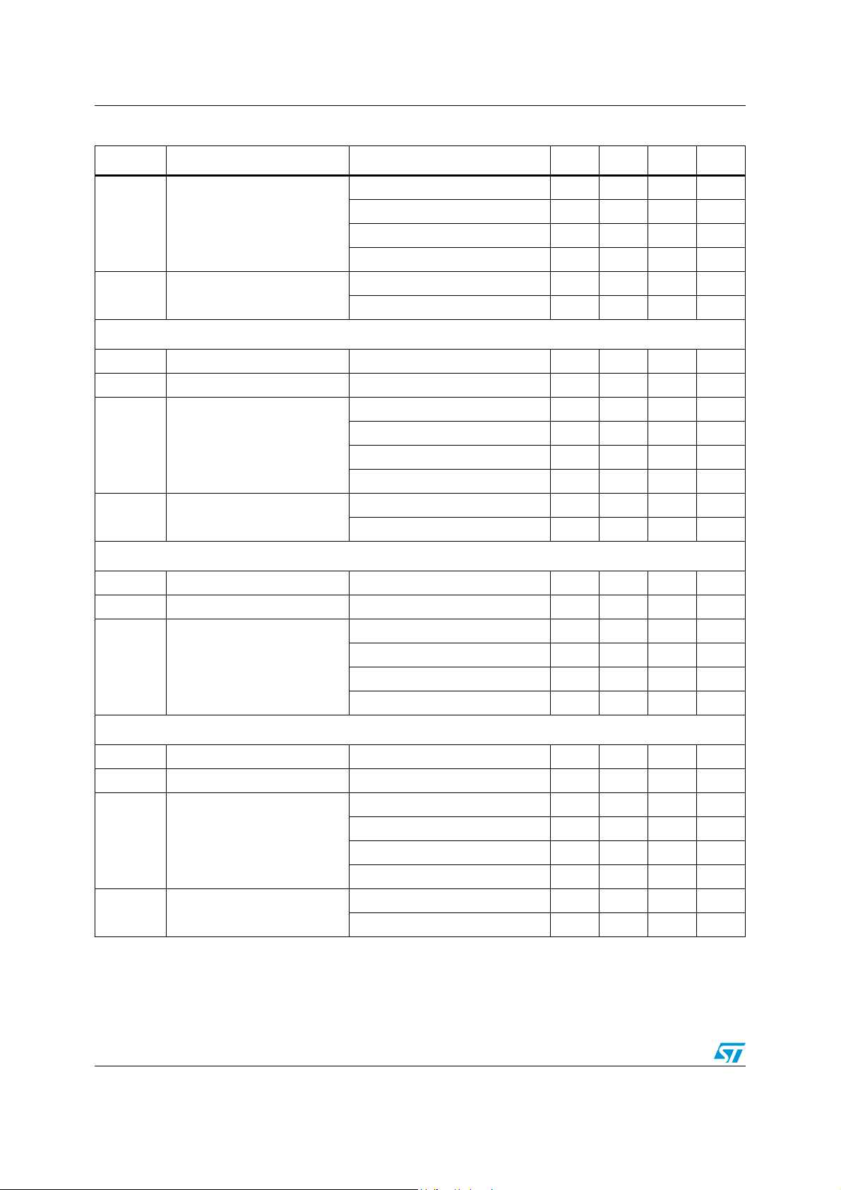
Page 36

Programming TDA7415CB
7.1 Data byte specification
The status after power-on reset is marked bold face / underlined in the programming tables.
Table 14. Main signal path input (addr. 00)
MSB LSB
D
7
---
111----- Unused, do not alter
Function
D
D
D
D
D
D
6
5
4
3
2
D
1
0
Input gain adjust level
0
0
0
0
0
0
0
0
0
1
0
0
0
1
1
1
1
1
:
:
:
:
1
1
1
0
1
1
1
1
1
1
1
1
1
1
1
0
:
:
:
:
0
0
0
1
0
0
0
0
–15dB
–14dB
…
–1dB
–0dB
+0dB
+1dB
…
+14dB
+15dB
Table 15. Main signal path, bass-filter (addr. 01)
MSB LSB
D
D
D
D
D
D
D
7
6
5
4
----
3
2
0
0
0
0
:
:
1
1
1
1
D
1
0
0
0
0
1
:
:
1
0
1
1
---01----
--01-----
0
0
0
1
1
0
1
1
------
Function
Level
0dB
1dB
:
14dB
15dB
Boost / Cut
Boost
Cut
Soft-step
On
Off
Quality factor
1.00
1.25
1.50
2.00
36/50 Doc ID 14100 Rev 3
Page 37

TDA7415CB Programming
Table 16. Main signal path, bass-filter (addr. 02)
MSB LSB
D
D
D
D
D
D
D
7
6
5
4
3
2
D
1
0
----1110Unused, do not alter
Center frequency
0
0
0
-
0
1
1
1
1
0
0
1
1
0
0
1
1
0
1
0
1
---0
1
0
1
150Hz
120Hz
100Hz
80Hz
70Hz
60Hz
50Hz
40Hz
DC-mode
0
1
Table 17. Main signal path, mid-filter (addr. 03)
-------
Off
On
MSB LSB
D
D
D
D
D
D
D
7
6
5
4
3
2
D
1
0
Function
Function
Level
0
0
0
0
15dB
0
0
0
1
----
:
:
:
1
1
1
1
1
1
14dB
:
:
0
1dB
1
0dB
Boost / Cut
---01----
Cut
Boost
Center frequency
0
-
0
1
1
0
1
----0
1
500Hz
1.0kHz
1.5kHz
2.0kHz
Quality factor
0
1
-------
1.0
2.0
Doc ID 14100 Rev 3 37/50
Page 38

Programming TDA7415CB
Table 18. Main signal path, treble-filter (addr. 04)
MSB LSB
D
D
D
D
D
D
D
7
6
5
4
3
2
D
1
0
Level
0
0
0
0
15dB
0
0
0
1
---:
:
:
1
1
1
1
1
1
14dB
:
:
0
1dB
1
0dB
Boost / Cut
---01----
Cut
Boost
Center frequency
0
-
0
1
1
0
1
----0
1
10kHz
12.5kHz
15kHz
17.5KHz
1-------Unused, do not alter
Table 19. Main signal path, room-EQ (addr. 05)
Function
MSB LSB
D
D
D
D
D
D
D
7
6
5
4
3
2
D
1
0
------10Unused, do not alter
Attenuation level
0
0
---
0
0
0
1
0
1
0
0
1
1
--
1
0
0
1
0
1
1
1
0
1
1
1
9dB
7dB
5.5dB
4dB
3dB
2dB
1dB
0dB
Center frequency
0
-
0
1
1
0
1
----0
1
240Hz
220Hz
200Hz
180Hz
Quality factor
0
1
------
1.0
2.0
Function
38/50 Doc ID 14100 Rev 3
Page 39

TDA7415CB Programming
Table 20. Input section, signal paths A-C (addr. 06-08)
MSB LSB
D
D
D
D
D
D
D
7
6
5
4
3
2
D
1
0
Input gain adjust level
0
0
0
0
0
–15dB
0
0
0
0
1
–14dB
---
0
0
0
1
1
1
1
1
:
:
:
:
…
1
1
1
0
–1dB
1
1
1
1
–0dB
1
1
1
1
+0dB
1
1
1
0
+1dB
:
:
:
0
0
0
0
0
0
…
:
+14dB
1
+15dB
0
Input select
0
0
0
0
0
1
0
1
1
0
1
0
1
1
1
1
0
1
0
1
----0
1
0
1
Tu ne r
CD
MD / Phone
CD-Changer (quasi-differential)
AUX./Navigation (quasi-differential)
Navigation (mono-Mix)
AC3in-monitor (from OUT-section)
Full mute
Function
Table 21. Input section; other settings (addr. 09)
MSB LSB
D
D
D
D
D
D
D
7
6
5
4
3
2
D
1
0
-0Unused, do not alter
Soft-mute, signal path A
------01-
No mute
Mute
Soft-mute, signal path B
-----01--
No mute
Mute
Soft-mute, signal path C
----01---
No mute
Mute
-11----Unused, do not alter
MD-mode
-01------
Single ended, stereo (e.g. Minidisk)
Full differential, mono
Fast-charge (quasi-differential inputs)
0
1
-------
Release
Engage
Function
(e.g. external Phone)
Doc ID 14100 Rev 3 39/50
Page 40

Programming TDA7415CB
Table 22. Output section, signal path 0 (addr. 10)
MSB LSB
D
D
D
D
D
D
D
7
6
5
4
3
2
D
1
0
Input select
0
Main signal path Output select
------00
1
AC0in
1
0
AC3in
1
1
Main signal path PRE-Tone select
Interrupts select, right channel
----00
0
1
--
1
0
1
1
Not allowed
Interrupt enable
Interrupt, 50% signal mix
Interrupt bypass
Interrupts select, left channel
--00
0
1
1
1
0
1
----
Not allowed
Interrupt enable
Interrupt, 50% signal mix
Interrupt bypass
-1------Unused, do not alter
Interrupt Pre-select (common for all paths)
0
1
-------
Navigation
Phone
Function
, normal operation
, normal operation
Table 23. Output section, signal path 1 and 2 (addr. 11)
MSB LSB
D
D
D
D
D
D
D
7
6
5
4
3
2
------00
-----01--
----01---
0
--00
1
1
1
---0
1
-01------
0
-------
1
D
1
0
Input select signal path1
0
Main signal path Output select
1
AC1in
1
0
AC3in
1
1
Main signal path PRE-Tone select
Interrupts select, right channel signal path 1
Interrupt enable
Interrupt bypass, normal operation
Interrupts select, left channel signal path 1
Interrupt enable
nterrupt bypass, normal operation
I
Input select signal path2
Main signal path Output select
AC2in
AC3in
Main signal path PRE-Tone select
Interrupts select, right channel signal path 2
Interrupt enable
Interrupt bypass, normal operation
Interrupts select, left channel signal path 2
Interrupt enable
Interrupt bypass, normal operation
Function
40/50 Doc ID 14100 Rev 3
Page 41

TDA7415CB Programming
Table 24. Output section, high-pass filters (addr. 12)
MSB LSB
D
D
D
D
D
D
D
7
6
5
4
3
2
D
1
0
Corner frequency, High-pass signal path 0
0
0
0
40 Hz
0
0
1
60 Hz
0
1
0
80 Hz
-----
0
1
1
100 Hz
1
0
0
120 Hz
1
0
1
150 Hz
1
1
0
180 Hz
1
1
1
220 Hz
Bypass, High-pass signal path 0
----01---
Filter bypass
Filter insert
Corner frequency, High-pass signal path 1
0
0
0
-
0
1
1
1
1
0
0
1
1
0
0
1
1
0
1
0
1
---0
1
0
1
40 Hz
60 Hz
80 Hz
100 Hz
120 Hz
150 Hz
180 Hz
220 Hz
Bypass, High-pass signal path 1
0
1
-------
Filter bypass
Filter insert
Function
Doc ID 14100 Rev 3 41/50
Page 42

Programming TDA7415CB
Table 25. Output section, volume 0L, 0R, 1L, 1R, 2L, 2R (addr. 13-16, 18, 19)
MSB LSB
Function
D
D
D
D
D
D
D
7
6
5
4
3
2
D
1
0
--------Volume level
1
1
1
0 0 0 1
-
-000
-001
-010
-011
-100
-101
-110
:
:
0
1
1
0
0
1
0
0
:
:
:
0
0
0
0
0
0
1
1
1
1
1
1
:
:
:
0
0
0
0
0
0
0
0
0
0
0
0
:
:
:
1
1
1
1
1
1
0
0
0
0
0
0
:
:
:
1
1
1
1
1
1
0
0
0
0
0
0
:
:
:
1
1
1
1
0
0
:
1
1
0
0
:
1
1
1
1
0
0
0
0
:
:
1
1
1
1
0
0
0
0
:
:
1
1
1
1
:
0
1
0
:
1
0
1
0
:
1
0
0
1
:
0
1
0
1
:
0
1
0
1
:
0
1
0
1
:
0
1
0
1
:
0
1
Not allowed
+25 dB
+24 dB
…
+17 dB
+16 dB
+15 dB
+14 dB
…
+1 dB
+0 dB
–0 dB
–1 dB
…
–14 dB
–15 dB
–16 dB
–17 dB
…
–30 dB
–31 dB
–32 dB
–33 dB
…
–46 dB
–47 dB
–48 dB
–49 dB
…
–62 dB
–63 dB
–64 dB
–65 dB
…
–78 dB
–79 dB
-111XXXXMute
Soft-step
0
1
-------
On
Off
42/50 Doc ID 14100 Rev 3
Page 43

TDA7415CB Programming
Table 26. Output section, subwoofer low-pass filter (addr. 17)
MSB LSB
D
D
D
D
D
D
D
7
6
5
4
3
2
D
1
0
-------0Unused, do not alter
Monitor select
X
0
----
0
X
0
1
0
1
0
1
1
0
X
1
1
Signal path 0 (before Soft-mute)
Signal path 1 (before Soft-mute)
Low-pass filter (Subwoofer enable)
Mono-sum bypass
Stereo bypass (direct through)
Corner frequency
0
0
-
0
0
1
1
0
0
1
1
X
1
0
1
0
---1
X
1
120 Hz
100 Hz
80 Hz
60 Hz
50 Hz
50 Hz
Phase
0
1
Table 27. Output section, bus-mutes (addr. 20)
-------
No shift
Inverted
MSB LSB
D
D
D
D
D
D
D
7
6
5
4
3
2
D
1
0
-------0Unused, do not alter
Soft-mute, right channel signal path 0
------01-
No mute
Mute
Soft-mute, left channel signal path 0
-----01--
No mute
Mute
Soft-mute, right channel signal path 1
----01---
No mute
Mute
Soft-mute, left channel signal path 1
---01----
No mute
Mute
Soft-mute, right channel signal path 2
--01-----
No mute
Mute
Soft-mute, left channel signal path 2
-01------
No mute
Mute
1-------Unused, do not alter
Function
Function
Doc ID 14100 Rev 3 43/50
Page 44

Programming TDA7415CB
Table 28. DC-detector and other output section settings (addr. 21)
MSB LSB
D
D
D
D
D
D
D
7
6
5
4
3
2
D
1
0
Line drivers gain
-------0
9dB
1
5.5dB
PAout0 (front) mute
------01-
No mute
Mute
PAout1 (rear) mute
-----01--
No mute
Mute
DCError output behavior
----01---
Forced high level by mute;
Normal operation, see description Chapter 5.5.
Zero-comparator Window size
--00
0
1
1
1
0
1
----
± 100mV
± 75mV
± 50mV
± 25mV
Function
(1)
Spike rejection time constant
0
0
0
1
1
0
1
1
1. DCError output high for OUTsection signal paths 1&2 muted or all PAout muted
------
11µs
22µs
33µs
44µs
44/50 Doc ID 14100 Rev 3
Page 45

TDA7415CB Programming
Table 29. Soft-mute and soft-step fader time (addr. 22)
MSB LSB
D
D
D
D
D
D
D
7
6
5
4
3
2
D
1
0
----1110Unused, do not alter
Input selection prcedure
----
0
---
1
Soft-mute completion time programmed according to
bits D6 and D7
Soft-mute completion time fixed to 0.5ms
Soft-step completion time
--00
0
1
1
1
0
1
----
0.32ms
0.64ms
1.28ms
2.56ms
Soft-mute completion time
0
0
0
1
1
0
1
1
Table 30. Spectrum analyzer settings (addr. 23)
------
0.25ms
0.5ms
10ms
5ms
Function
MSB LSB
D
D
D
D
D
D
D
7
6
5
4
3
2
D
1
0
Run/stop (internal clocking)
-------0
Stop
1
Run
Filter quality
------01-
High
Low
Reset mode
-----01--
SAres-pin triggered reset
Auto-reset mode
Source select
----01---
Mono-sum of MUXA-outputs
SAin-pin
1111- - --Unused, do not alter
Function
Doc ID 14100 Rev 3 45/50
Page 46

Programming TDA7415CB
Table 31. Testing * (addr. 31)
MSB LSB
D6D5D4D3D2D1D
D
7
0
Device clock
-------0
Enable internal clock generation
1
Allow external clocking in fast-mode
----111-Unused, do not alter
--------Test selector
TUNER L out:
0
0
0
0
0
1
0
1
0
-
0
1
1
----
1
0
0
1
0
1
1
1
0
1
1
1
DCDet., lower TC-Vth
Spec.Anal. 60Hz-bandpass
Spec.Anal. 160Hz-bandpass
Spec.Anal. 400Hz-bandpass
Spec.Anal. 1kHz-bandpass
Spec.Anal. 2,5kHz-bandpass
Spec.Anal. 6,3kHz-bandpass
Spec.Anal. 16kHz-bandpass
Test mode
0
-------
1
Enabled
Disabled
*
Function
TUNER R out:
DCDet., upper TC-Vth
5,5V CMOS-supply
DCDet., time constant
200kHz reference clock
actual Soft-Mute clock
actual Soft-Step clock
SC-reference, left chan.
DC-Offset monitor point
Successfully entering the test-mode requires to set bit D6 of the sub address (test mode-bit)
to "1". In test-mode, the TUNER L&R inputs are reconfigured as output for the selected test
signals
Note: This byte is used for testing and/or evaluation purposes only and must not be set to other
values than the default "11111110" in the application.
46/50 Doc ID 14100 Rev 3
Page 47

TDA7415CB Application information
8 Application information
Figure 27. Typical application connections diagram
68
Figure 27 shows a proposal for a typical application. - However, the figure only represents
one possible interconnection scheme with other devices (The shaded blocks could
represent a complex digital sound reproducing/processing system). For simplicity, this
proposal assumes the system designer not to take advantage from the direct muting feature
and therefore let the corresponding Mute-pins floating.
All capacitor values are suggestions with their dimensioning still being dependant on girdling
impedances. This is especially true for the capacitors located at the WinTC-pins as can be
read in chapter 6.5. In case the DC-detector function is not assessed in the application
it is recommended to short both the WinTC-pins 14 and 15 to device-ground.
Doc ID 14100 Rev 3 47/50
Page 48

Package information TDA7415CB
9 Package information
In order to meet environmental requirements, ST offers these devices in different grades of
ECOPACK
®
packages, depending on their level of environmental compliance. ECOPACK
®
specifications, grade definitions and product status are available at: www.st.com.
ECOPACK
®
is an ST trademark.
Figure 28. LQFP64 mechanical data and package dimensions
DIM.
A 1.60 0.063
A1 0.05 0.15 0.002 0.006
A2 1.35 1.40 1.45 0.053 0.055 0.057
B 0.17 0.22 0.27 0.0066 0.0086 0.0106
C 0.09 0 .0035
D 11.80 12.00 12.20 0.464 0.472 0.480
D1 9.80 10.00 10.20 0.386 0.394 0.401
D3 7.50 0.295
e 0.50 0.0197
E 11.80 12.00 12.20 0.464 0.472 0.480
E1 9.80 10.00 10.20 0.386 0.394 0.401
E3 7.50 0.295
L 0.45 0.60 0.75 0.0177 0.0236 0.0295
L1 1.00 0.0393
K 0˚ (m in.), 3.5˚ (typ.), 7˚ (max.)
ccc 0.080 0.0031
mm inch
MIN. TYP. MAX. MIN. TYP. MAX.
OUTLINE AND
MECHANICAL DATA
LQFP64 (10 x 10 x 1.4mm)
D
D1
48
49
B
64
1
e
33
32
E3D3E1
17
16
48/50 Doc ID 14100 Rev 3
A
A2
A1
0.08mm
ccc
Seating Plane
B
E
C
L1
L
K
0051434 F
Page 49

TDA7415CB Revision history
10 Revision history
Table 32. Document revision history
Date Revision Changes
26-Oct-2007 1 Initial release.
24-Nov-2008 2 Updated the Table 8: Output section on page 15.
24-Jun-2009 3
Updated Figure 28: LQFP64 mechanical data and package
dimensions on page 48.
Doc ID 14100 Rev 3 49/50
Page 50

TDA7415CB
Please Read Carefully:
Information in this document is provided solely in connection with ST products. STMicroelectronics NV and its subsidiaries (“ST”) reserve the
right to make changes, corrections, modifications or improvements, to this document, and the products and services described herein at any
time, without notice.
All ST products are sold pursuant to ST’s terms and conditions of sale.
Purchasers are solely responsible for the choice, selection and use of the ST products and services described herein, and ST assumes no
liability whatsoever relating to the choice, selection or use of the ST products and services described herein.
No license, express or implied, by estoppel or otherwise, to any intellectual property rights is granted under this document. If any part of this
document refers to any third party products or services it shall not be deemed a license grant by ST for the use of such third party products
or services, or any intellectual property contained therein or considered as a warranty covering the use in any manner whatsoever of such
third party products or services or any intellectual property contained therein.
UNLESS OTHERWISE SET FORTH IN ST’S TERMS AND CONDITIONS OF SALE ST DISCLAIMS ANY EXPRESS OR IMPLIED
WARRANTY WITH RESPECT TO THE USE AND/OR SALE OF ST PRODUCTS INCLUDING WITHOUT LIMITATION IMPLIED
WARRANTIES OF MERCHANTABILITY, FITNESS FOR A PARTICULAR PURPOSE (AND THEIR EQUIVALENTS UNDER THE LAWS
OF ANY JURISDICTION), OR INFRINGEMENT OF ANY PATENT, COPYRIGHT OR OTHER INTELLECTUAL PROPERTY RIGHT.
UNLESS EXPRESSLY APPROVED IN WRITING BY AN AUTHORIZED ST REPRESENTATIVE, ST PRODUCTS ARE NOT
RECOMMENDED, AUTHORIZED OR WARRANTED FOR USE IN MILITARY, AIR CRAFT, SPACE, LIFE SAVING, OR LIFE SUSTAINING
APPLICATIONS, NOR IN PRODUCTS OR SYSTEMS WHERE FAILURE OR MALFUNCTION MAY RESULT IN PERSONAL INJURY,
DEATH, OR SEVERE PROPERTY OR ENVIRONMENTAL DAMAGE. ST PRODUCTS WHICH ARE NOT SPECIFIED AS "AUTOMOTIVE
GRADE" MAY ONLY BE USED IN AUTOMOTIVE APPLICATIONS AT USER’S OWN RISK.
Resale of ST products with provisions different from the statements and/or technical features set forth in this document shall immediately void
any warranty granted by ST for the ST product or service described herein and shall not create or extend in any manner whatsoever, any
liability of ST.
ST and the ST logo are trademarks or registered trademarks of ST in various countries.
Information in this document supersedes and replaces all information previously supplied.
The ST logo is a registered trademark of STMicroelectronics. All other names are the property of their respective owners.
© 2009 STMicroelectronics - All rights reserved
STMicroelectronics group of companies
Australia - Belgium - Brazil - Canada - China - Czech Republic - Finland - France - Germany - Hong Kong - India - Israel - Italy - Japan -
Malaysia - Malta - Morocco - Philippines - Singapore - Spain - Sweden - Switzerland - United Kingdom - United States of America
www.st.com
50/50 Doc ID 14100 Rev 3
 Loading...