

Page 1
Features
■ 4 stereo inputs
■ 1 mono input
■ Soft-step volume
■ Bass, Treble and Loudness control
■ D i r e c t - m u t e a n d s o f t - m u t e
■ Internal beep
■ Four independent speaker outputs
■ Subwoofer stereo output
■ Digital control:
2
–I
C bus interface
– Audio filter characteristics programmable
Description
The TDA7404 is a high performance signal
processor specifically designed for car radio
applications.
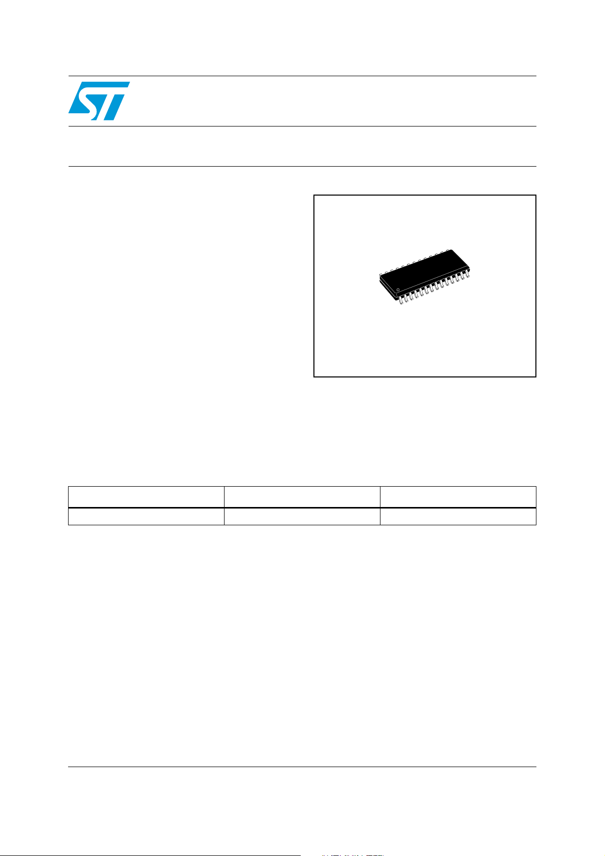
Table 1. Device summary
TDA7404
Car radio signal processor
SO-28
The device includes a high performance
audioprocessor with fully integrated audio filters.
The digital control allows a programming in a wide
range of all the filter characteristics. By the use of
a BiCMOS process and a linear signal processing
low distortion and low noise are obtained.
Order code Package Packing
TDA7404D SO-28 Tube
December 2008 Rev 2 1/35
www.st.com
1
Page 2

Contents TDA7404
Contents
1 Detailed features . . . . . . . . . . . . . . . . . . . . . . . . . . . . . . . . . . . . . . . . . . . . 6
2 Block and pin description diagrams . . . . . . . . . . . . . . . . . . . . . . . . . . . . 7
3 Electrical specifications . . . . . . . . . . . . . . . . . . . . . . . . . . . . . . . . . . . . . . 8
3.1 Supply . . . . . . . . . . . . . . . . . . . . . . . . . . . . . . . . . . . . . . . . . . . . . . . . . . . . 8
3.2 Thermal data . . . . . . . . . . . . . . . . . . . . . . . . . . . . . . . . . . . . . . . . . . . . . . . 8
3.3 Absolute maximum ratings . . . . . . . . . . . . . . . . . . . . . . . . . . . . . . . . . . . . . 8
3.4 ESD . . . . . . . . . . . . . . . . . . . . . . . . . . . . . . . . . . . . . . . . . . . . . . . . . . . . . . 8
3.5 Electrical characteristics . . . . . . . . . . . . . . . . . . . . . . . . . . . . . . . . . . . . . . . 9
4 Description of functionality . . . . . . . . . . . . . . . . . . . . . . . . . . . . . . . . . . 13
4.1 Input stages . . . . . . . . . . . . . . . . . . . . . . . . . . . . . . . . . . . . . . . . . . . . . . . 13
4.2 AutoZero . . . . . . . . . . . . . . . . . . . . . . . . . . . . . . . . . . . . . . . . . . . . . . . . . . 14
4.2.1 AutoZero remain . . . . . . . . . . . . . . . . . . . . . . . . . . . . . . . . . . . . . . . . . . 14
4.3 Mixing stage . . . . . . . . . . . . . . . . . . . . . . . . . . . . . . . . . . . . . . . . . . . . . . . 14
4.4 Loudness . . . . . . . . . . . . . . . . . . . . . . . . . . . . . . . . . . . . . . . . . . . . . . . . . 15
4.4.1 Attenuation . . . . . . . . . . . . . . . . . . . . . . . . . . . . . . . . . . . . . . . . . . . . . . . 15
4.4.2 Center frequency . . . . . . . . . . . . . . . . . . . . . . . . . . . . . . . . . . . . . . . . . . 15
4.4.3 Low and high frequency boost . . . . . . . . . . . . . . . . . . . . . . . . . . . . . . . . 16
4.5 Soft-mute . . . . . . . . . . . . . . . . . . . . . . . . . . . . . . . . . . . . . . . . . . . . . . . . . 16
4.6 Soft-step volume . . . . . . . . . . . . . . . . . . . . . . . . . . . . . . . . . . . . . . . . . . . 17
4.7 Bass . . . . . . . . . . . . . . . . . . . . . . . . . . . . . . . . . . . . . . . . . . . . . . . . . . . . . 17
4.7.1 Attenuation . . . . . . . . . . . . . . . . . . . . . . . . . . . . . . . . . . . . . . . . . . . . . . . 17
4.7.2 Center frequency . . . . . . . . . . . . . . . . . . . . . . . . . . . . . . . . . . . . . . . . . . 18
4.7.3 Quality factors . . . . . . . . . . . . . . . . . . . . . . . . . . . . . . . . . . . . . . . . . . . . 18
4.7.4 DC mode . . . . . . . . . . . . . . . . . . . . . . . . . . . . . . . . . . . . . . . . . . . . . . . . 19
4.8 Treble . . . . . . . . . . . . . . . . . . . . . . . . . . . . . . . . . . . . . . . . . . . . . . . . . . . . 20
4.8.1 Attenuation . . . . . . . . . . . . . . . . . . . . . . . . . . . . . . . . . . . . . . . . . . . . . . . 20
4.8.2 Center frequency . . . . . . . . . . . . . . . . . . . . . . . . . . . . . . . . . . . . . . . . . . 20
4.9 External AC - coupling . . . . . . . . . . . . . . . . . . . . . . . . . . . . . . . . . . . . . . . 21
4.10 Speaker attenuator . . . . . . . . . . . . . . . . . . . . . . . . . . . . . . . . . . . . . . . . . . 21
4.11 Subwoofer attenuator . . . . . . . . . . . . . . . . . . . . . . . . . . . . . . . . . . . . . . . . 21
2/35
Page 3

TDA7404 Contents
5 I2C bus interface . . . . . . . . . . . . . . . . . . . . . . . . . . . . . . . . . . . . . . . . . . . 22
5.1 Interface protocol . . . . . . . . . . . . . . . . . . . . . . . . . . . . . . . . . . . . . . . . . . . 22
5.2 Transmitted data (send mode) . . . . . . . . . . . . . . . . . . . . . . . . . . . . . . . . . 22
5.3 Reset condition . . . . . . . . . . . . . . . . . . . . . . . . . . . . . . . . . . . . . . . . . . . . . 22
5.4 Subaddress (receive mode) . . . . . . . . . . . . . . . . . . . . . . . . . . . . . . . . . . . 23
5.5 Data byte specification . . . . . . . . . . . . . . . . . . . . . . . . . . . . . . . . . . . . . . . 24
6 Application circuit . . . . . . . . . . . . . . . . . . . . . . . . . . . . . . . . . . . . . . . . . . 32
7 Package information . . . . . . . . . . . . . . . . . . . . . . . . . . . . . . . . . . . . . . . . 33
8 Revision history . . . . . . . . . . . . . . . . . . . . . . . . . . . . . . . . . . . . . . . . . . . 34
3/35
Page 4

List of tables TDA7404
List of tables
Table 1. Device summary . . . . . . . . . . . . . . . . . . . . . . . . . . . . . . . . . . . . . . . . . . . . . . . . . . . . . . . . . . 1
Table 2. Supply . . . . . . . . . . . . . . . . . . . . . . . . . . . . . . . . . . . . . . . . . . . . . . . . . . . . . . . . . . . . . . . . . . 8
Table 3. Thermal data. . . . . . . . . . . . . . . . . . . . . . . . . . . . . . . . . . . . . . . . . . . . . . . . . . . . . . . . . . . . . 8
Table 4. Absolute maximum ratings . . . . . . . . . . . . . . . . . . . . . . . . . . . . . . . . . . . . . . . . . . . . . . . . . . 8
Table 5. Electrical characteristics . . . . . . . . . . . . . . . . . . . . . . . . . . . . . . . . . . . . . . . . . . . . . . . . . . . . 9
Table 6. Others selection . . . . . . . . . . . . . . . . . . . . . . . . . . . . . . . . . . . . . . . . . . . . . . . . . . . . . . . . . 21
Table 7. Subaddress (receive mode) . . . . . . . . . . . . . . . . . . . . . . . . . . . . . . . . . . . . . . . . . . . . . . . . 23
Table 8. Input selector / gain . . . . . . . . . . . . . . . . . . . . . . . . . . . . . . . . . . . . . . . . . . . . . . . . . . . . . . 24
Table 9. Loudness . . . . . . . . . . . . . . . . . . . . . . . . . . . . . . . . . . . . . . . . . . . . . . . . . . . . . . . . . . . . . . 25
Table 10. Volume . . . . . . . . . . . . . . . . . . . . . . . . . . . . . . . . . . . . . . . . . . . . . . . . . . . . . . . . . . . . . . . . 25
Table 11. Treble programming . . . . . . . . . . . . . . . . . . . . . . . . . . . . . . . . . . . . . . . . . . . . . . . . . . . . . . 26
Table 12. Bass programming . . . . . . . . . . . . . . . . . . . . . . . . . . . . . . . . . . . . . . . . . . . . . . . . . . . . . . . 27
Table 13. Speaker attenuator left front . . . . . . . . . . . . . . . . . . . . . . . . . . . . . . . . . . . . . . . . . . . . . . . . 28
Table 14. Speaker attenuator right front . . . . . . . . . . . . . . . . . . . . . . . . . . . . . . . . . . . . . . . . . . . . . . . 28
Table 15. Speaker attenuator left rear . . . . . . . . . . . . . . . . . . . . . . . . . . . . . . . . . . . . . . . . . . . . . . . . 29
Table 16. Speaker attenuator right rear . . . . . . . . . . . . . . . . . . . . . . . . . . . . . . . . . . . . . . . . . . . . . . . 29
Table 17. Subwoofer attenuator (left and right) . . . . . . . . . . . . . . . . . . . . . . . . . . . . . . . . . . . . . . . . 30
Table 18. Soft-mute and mixing . . . . . . . . . . . . . . . . . . . . . . . . . . . . . . . . . . . . . . . . . . . . . . . . . . . . . 30
Table 19. Others . . . . . . . . . . . . . . . . . . . . . . . . . . . . . . . . . . . . . . . . . . . . . . . . . . . . . . . . . . . . . . . . . 31
Table 20. Testing . . . . . . . . . . . . . . . . . . . . . . . . . . . . . . . . . . . . . . . . . . . . . . . . . . . . . . . . . . . . . . . . 31
Table 21. Document revision history . . . . . . . . . . . . . . . . . . . . . . . . . . . . . . . . . . . . . . . . . . . . . . . . . 34
4/35
Page 5

TDA7404 List of figures
List of figures
Figure 1. Block diagram . . . . . . . . . . . . . . . . . . . . . . . . . . . . . . . . . . . . . . . . . . . . . . . . . . . . . . . . . . . . 7
Figure 2. Pin connection (top view) . . . . . . . . . . . . . . . . . . . . . . . . . . . . . . . . . . . . . . . . . . . . . . . . . . . 7
Figure 3. Input stages diagram . . . . . . . . . . . . . . . . . . . . . . . . . . . . . . . . . . . . . . . . . . . . . . . . . . . . . 13
Figure 4. Signal-flow of mixing-stage . . . . . . . . . . . . . . . . . . . . . . . . . . . . . . . . . . . . . . . . . . . . . . . . . 14
Figure 5. Loudness attenuation @ fC = 400 Hz. . . . . . . . . . . . . . . . . . . . . . . . . . . . . . . . . . . . . . . . . 15
Figure 6. Loudness center frequencies @ Attn. = 15 dB . . . . . . . . . . . . . . . . . . . . . . . . . . . . . . . . . . 15
Figure 7. Loudness attenuation, fC = 2.4 kHz . . . . . . . . . . . . . . . . . . . . . . . . . . . . . . . . . . . . . . . . . . 16
Figure 8. Soft-mute timing . . . . . . . . . . . . . . . . . . . . . . . . . . . . . . . . . . . . . . . . . . . . . . . . . . . . . . . . . 16
Figure 9. Soft-step timing . . . . . . . . . . . . . . . . . . . . . . . . . . . . . . . . . . . . . . . . . . . . . . . . . . . . . . . . . . 17
Figure 10. Bass control @ f
Figure 11. Bass center frequencies @ gain = 15 dB, Q = 1 . . . . . . . . . . . . . . . . . . . . . . . . . . . . . . . . 18
Figure 12. Bass quality factors @ gain = 14 dB, f
Figure 13. Bass normal and DC mode @ gain = 14 dB, fC = 80 Hz . . . . . . . . . . . . . . . . . . . . . . . . . . 19
Figure 14. Treble control @ fC = 17.5kHz . . . . . . . . . . . . . . . . . . . . . . . . . . . . . . . . . . . . . . . . . . . . . . 20
Figure 15. Treble center frequencies @ Gain = 15 dB . . . . . . . . . . . . . . . . . . . . . . . . . . . . . . . . . . . . 20
Figure 16. External AC coupling . . . . . . . . . . . . . . . . . . . . . . . . . . . . . . . . . . . . . . . . . . . . . . . . . . . . . 21
Figure 17. Software specification . . . . . . . . . . . . . . . . . . . . . . . . . . . . . . . . . . . . . . . . . . . . . . . . . . . . . 22
Figure 18. TDA7404 application circuit . . . . . . . . . . . . . . . . . . . . . . . . . . . . . . . . . . . . . . . . . . . . . . . . 32
Figure 19. SO-28 mechanical data and package dimensions . . . . . . . . . . . . . . . . . . . . . . . . . . . . . . . 33
= 80 Hz, Q = 1 . . . . . . . . . . . . . . . . . . . . . . . . . . . . . . . . . . . . . . . . . . . . 17
C
= 80 Hz . . . . . . . . . . . . . . . . . . . . . . . . . . . . . . . . 18
C
5/35
Page 6

Detailed features TDA7404
1 Detailed features
● Input multiplexer
– 1 pseudo-differential stereo input (selectable single end stereo input)
– 3 single-end stereo inputs
– 1 differential mono input
– In-Gain 0..14 dB, 1 dB steps, 14..20 dB, 2 dB steps
– Auto Zero
● Beep
– internal beep with 3 frequencies
– 781 Hz/1.56 kHz/1.8 kHz
● Mixing stage
– 4 step-mixing-stage with mono or beep as mix-signals
● Loudness
– second order frequency response
– programmable center frequency
– 15 x 1 dB steps
– selectable low and high frequency boost
– selectable flat-mode (constant attenuation)
● Vol u me
– 1 dB attenuator
– 100 dB range
– soft-step control with programmable times
● Bass
● Tre bl e
● Speaker
● Subwoofer
● Mute functions
nd
–2
order frequency response
– center frequency programmable in 4 steps
– 60 Hz / 80 Hz / 100 Hz / 200 Hz
– Q programmable 1.0/1.25/1.5/2.0
– DC gain programmable
–+
15 dB x 1 dB steps
nd
–2
order frequency response
– center frequency programmable in 4 steps
– 10 kHz / 12.5 kHz / 15 kHz / 17.5 kHz
–+
15 dB x 1 dB steps
– 4 independent speaker controls in 1 dB steps
– control range 50 dB with mute
– Zero crossing attenuate
– Stereo output
– attenuator range 50 dB
–direct mute
– digitally controlled Soft Mute with 4 programmable mute-times
6/35
Page 7
TDA7404 Block and pin description diagrams
p
p
X
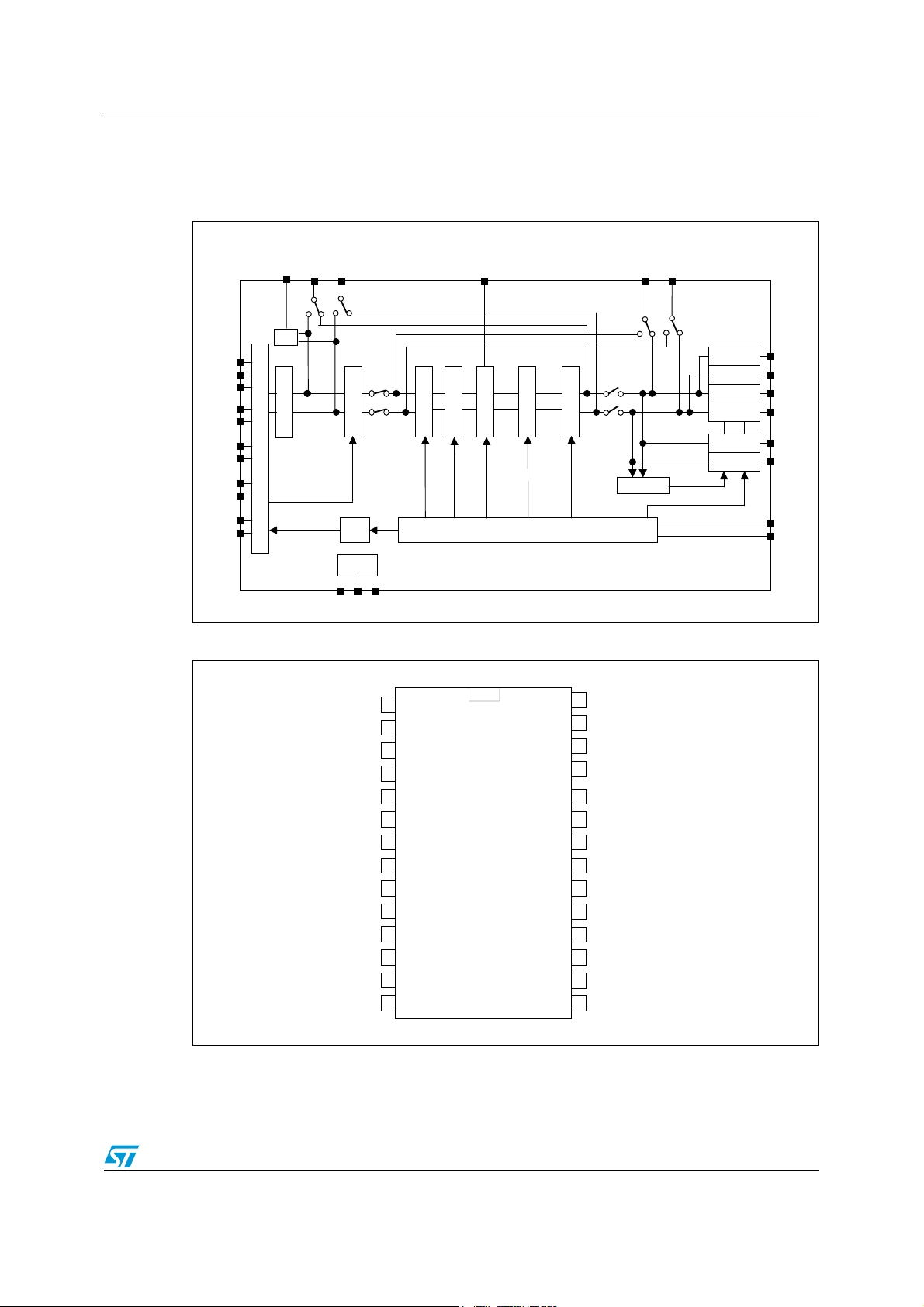
2 Block and pin description diagrams
Figure 1. Block diagram
COUTL
DiffinL
Diffgnd
DiffinR
SE1L
SE1R
SE2L
SE2R
SE3L
SE3R
Mono+
Mono -
lexer
ut Multi
In
MU
MIX
Gain/Auto Zero
Mono/Beep
COUTR
Mixing St age
Loudness
MUTE
Bass
Volu me
Treble
Soft Mute
Digital Control I2C-BusBeep
CINL
Zero Cross
CINR
Mono Fader
Mono Fader
Mono Fader
Mono Fader
Mono Fader
Mono Fader
Out LF
Out RF
Out LR
Out RR
SW L
SW R
SCL
SDA
Supply
VrefGnd Vcc
Figure 2. Pin connection (top view)
SE1L
SE1R
SE2L
SE2R
SE3L
SE3R
Mono+
Mono-
DiffinR
Difffgnd
DiffinL
ACINR
ACINL
CREF
1
2
3
4
5
6
7
8
9
10
11
12
13
14
ACOU TL
28
ACOU TR
27
VDD
26
SDA
25
SCL
24
MUTE
23
MUX
22
OUTLF
21
OUTLR
20
OUTRR
19
OUTRF
18
SWL
17
SWR
16
GND
15
7/35
Page 8
Electrical specifications TDA7404
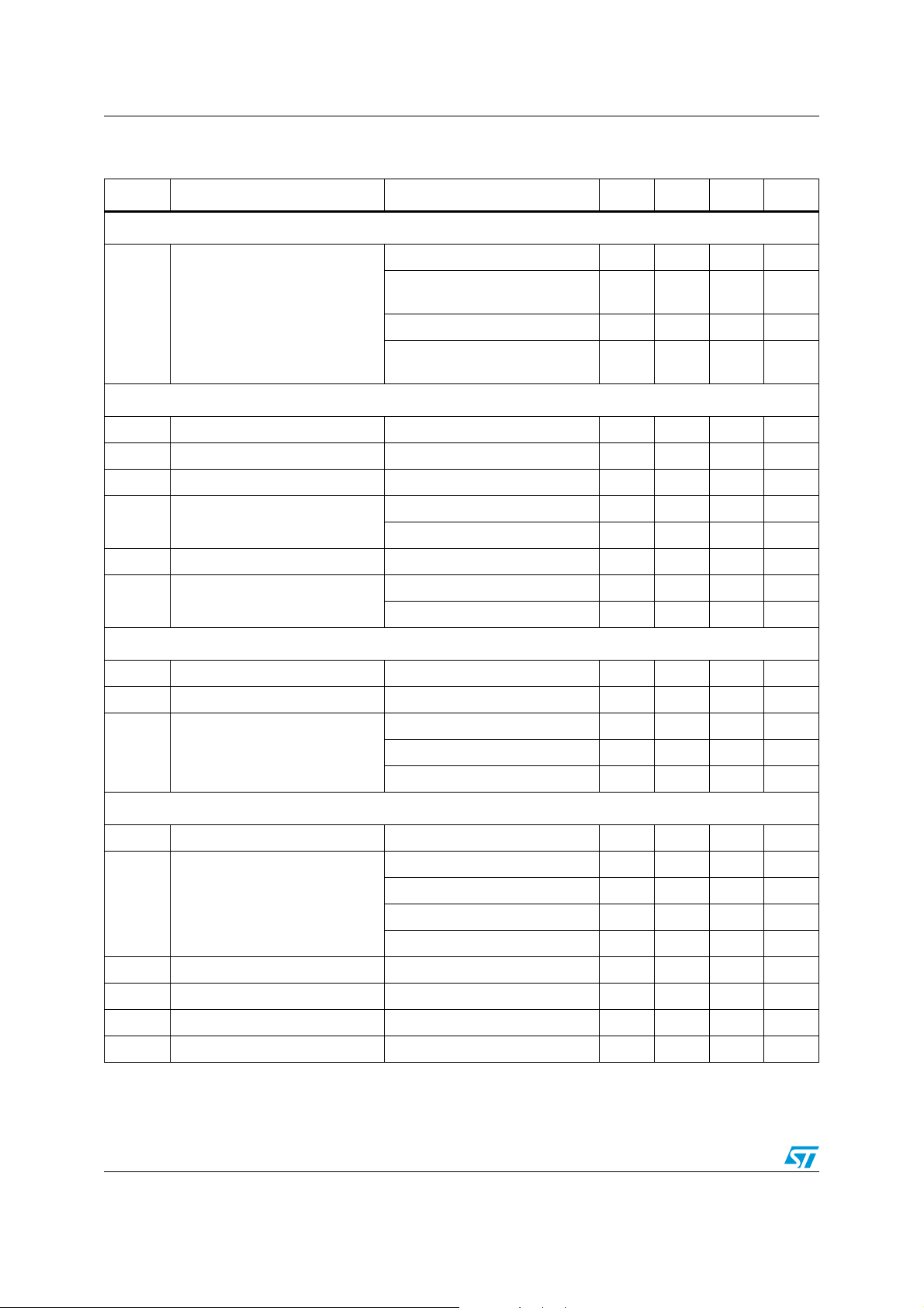
3 Electrical specifications
3.1 Supply
Table 2. Supply
Symbol Parameter Test condition Min. Typ. Max. Unit
V
Supply voltage 7.5 9 10.5 V
s
Supply current Vs = 9V 20 mA
I
s
SVRR Ripple rejection @ 1 kHz Audioprocessor (all Filters flat) 60 dB
3.2 Thermal data
Table 3. Thermal data
Symbol Parameter Value Unit
R
Th j-pins
Thermal resistance junction pins max 85 °C/W
3.3 Absolute maximum ratings
Table 4. Absolute maximum ratings
Symbol Parameter Value Unit
T
V
amb
T
s
stg
Operating supply voltage 10.8 V
Operating temperature range -40 to 85 °C
Storage temperature range -55 to +150 °C
3.4 ESD
All pins are protected against ESD according to the MIL883 standard.
8/35
Page 9
TDA7404 Electrical specifications
3.5 Electrical characteristics
Table 5. Electrical characteristics
(V
=9 V; T
S
=25 °C; RL=10 kΩ; all gains = 0 dB; f = 1 kHz; unless otherwise specified)
amb
Symbol Parameter Test conditions Min. Typ. Max. Unit
Input selector
V
S
G
IN MIN
G
IN MAX
G
R
STEP
Input resistance all single ended Inputs 70 100 130 kΩ
in
Clipping level 2.20 2.60 V
CL
Input separation 80 100 dB
IN
Min. input gain -1 0 1 dB
Max. input gain 18 20 22 dB
Step Resolution 0.5 1 1.5 dB
Adjacent gain steps -5 1 5 mV
V
V
offset
DC Steps
DC
G
MIN
to G
MAX
-10 5 10 mV
Remaining offset with AutoZero 0.5 mV
P differential stereo inputs
R
Input resistance
in
(see Figure 3)
Differential 70 100 130 kΩ
-0.75 0 0.75 dB
CD
Gain
G
only at true differential
input
-5 -6 -7 dB
-11 -12 -13 dB
V
CMRR Common mode rejection ratio
e
Output noise @ speaker-outputs
NO
= 1 V
CM
V
= 1 V
CM
20 Hz - 20 kHz, flat;
all stages 0 dB
@ 1 kHz 40 70 dB
RMS
@ 10 kHz 40 60 dB
RMS
9V
RMS
Differential mono input
R
Input resistance Differential 395673kΩ
in
CMRR Common mode rejection ratio
Beep control
V
Beep level 250 350 500 mV
RMS
f
Beep frequency
B
V
= 1 V
CM
= 1 V
V
CM
f
B1
f
B2
f
B3
@ 1 kHz 40 70 dB
RMS
@ 10 kHz 40 60 dB
RMS
740 781 820 Hz
1.48 1.56 1.64 kHz
1.7 1.8 1.9 kHz
9/35
Page 10
Electrical specifications TDA7404
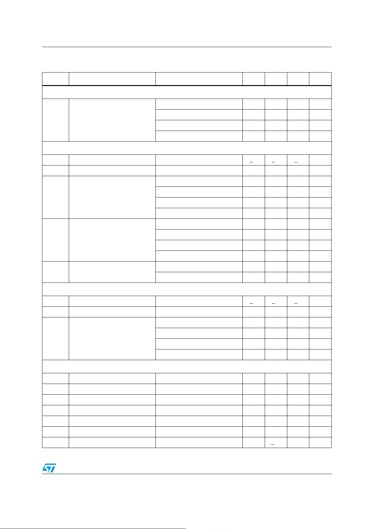
Table 5. Electrical characteristics (continued)
(V
=9 V; T
S
Symbol Parameter Test conditions Min. Typ. Max. Unit
Mixing control
=25 °C; RL=10 kΩ; all gains = 0 dB; f = 1 kHz; unless otherwise specified)
amb
Main / mix-source 0/00 dB
M
LEVEL
Mixing level
Volu m e co n t rol
G
A
A
V
STEP
E
Max. gain 283032 dB
MAX
Max. attenuation -83 -79 -75 dB
MAX
Step resolution 0.5 1 1.5 dB
Attenuation set error
A
Tracking error 2 dB
E
T
DC steps
DC
Loudness control
A
A
STEP
Step resolution -0.5 1 1.5 dB
Max. attenuation 13 15 17 dB
MAX
f
Center frequency
C
Main / mix-source
-8.5/-
10.6
-3.5/-
9.6
-2.5/-
8.6
dB
Main / mix-source -5/-5 -6/-6 -7/-7 dB
Main / mix-source
-11/-
1.5
-12/-
2.5
-13/-
3.5
dB
G = -20 to +20 dB -1 0 1 dB
G = -80 to -20 dB -4 0 3 dB
Adjacent steps 0.1 3 mV
From 0 dB to G
MIN
0.5 5 mV
360 400 440 Hz
720 800 880 Hz
2.3 2.4
(1)
2.5 kHz
Soft-mute
A
MUTE
Mute attenuation 80 100 dB
T1 0.48 1 ms
T2 0.96 2 ms
Delay time
T
D
T3 20 30.7 50 ms
T4 70 123 170 ms
V
TH low
V
TH high
R
V
Low threshold for SM pin
High threshold for SM pin 2.50 V
Internal pull-up resistor 70 100 130 kΩ
PU
Pull-up voltage 5 V
PU
(2)
10/35
1V
Page 11
TDA7404 Electrical specifications
Table 5. Electrical characteristics (continued)
(V
=9 V; T
S
Symbol Parameter Test conditions Min. Typ. Max. Unit
Soft-step
=25 °C; RL=10 kΩ; all gains = 0 dB; f = 1 kHz; unless otherwise specified)
amb
T
SW
Switch time
Bass control
C
RANGE
A
STEP
Q
BASS
DC
Control range +14 +15 +16 dB
Step resolution 0.5 1 1.5 dB
Center frequency
f
C
Quality factor
Bass DC gain
GAIN
T
T
T
T
f
f
f
f
Q
Q
Q
Q
SW1
SW2
SW3
SW4
C1
C2
C3
C4
54 60 66 Hz
72 80 88 Hz
90 100 110 Hz
180 200 220 Hz
1
2
3
4
0.911.1
1.11.251.4
1.3 1.5 1.7
1.822.2
0.68 ms
1.26 ms
2.52 ms
5.04 ms
DC = off -1 0 1 dB
DC = on 4 4.4 6 dB
Treble control
C
RANGE
A
STEP
Control range +14 +15 +16 dB
Step resolution 0.5 1 1.5 dB
Center frequency
f
C
Speaker attenuator
C
RANGE
A
STEP
A
MUTE
E
V
T
V
Control range -53 50 -47 dB
Step resolution Only for attenuation up to 24 dB 0.5 1 1.5 dB
Output mute attenuation 80 90 dB
Attenuation set error -2 2 dB
E
DC steps Adjacent attenuation steps 0.10 5 mV
DC
Zero cross timer Data bit D1=1, D2=1 29 37 45 ms
ZC
Zero cross threshold +20 mV
th
f
C1
f
C2
f
C3
f
C4
81012kHz
10 12.5 15 kHz
12 15 18 kHz
14 17.5 21 kHz
11/35
Page 12

Electrical specifications TDA7404
Table 5. Electrical characteristics (continued)
(V
=9 V; T
S
Symbol Parameter Test conditions Min. Typ. Max. Unit
Fader outputs
=25 °C; RL=10 kΩ; all gains = 0 dB; f = 1 kHz; unless otherwise specified)
amb
V
R
V
Clipping level d = 0.3% 2.20 2.60 V
CLIP
R
Output load resistance 2 kΩ
L
Output load capacitance 10 nF
C
L
Output impedance 30 100 W
OUT
DC Voltage Level 4.3 4.5 4.7 V
DC
Subwoofer attenuator
C
RANGE
A
STEP
A
MUTE
E
V
Control range -53 50 -47 dB
Step resolution 0.5 1 1.5 dB
Output mute attenuation 80 90 dB
Attenuation set error 2 dB
E
DC steps Adjacent attenuation steps 0.10 5 mV
DC
General
BW = 20 Hz - 20 kHz
e
NO
Output noise
all gains = 0 dB single ended
inputs
all gains = 0 dB
S/N Signal to noise ratio
flat; VO = 2V
RMS
bass, treble at +12 dB;
a-weighted; VO = 2.6 V
V
= 1 V
IN
; all stages 0 dB
RMS
RMS
internal pass only
d Distortion
V
OUT
= 1 V
RMS
;
Bass and treble = 12 dB
S
1. The SM-Pin is active low (Mute = 0).
2. Center frequency 2.4 kHz makes 1kHz bottom frequency at low and high frequency boost condition.
Channel separation left/right 80 100 dB
C
A
= 0 to -20 dB -1 0 1 dB
E
Total tracking error
T
V
A
= -20 to -60 dB -2 0 2 dB
V
RMS
10 15 μV
106 dB
100 dB
0.005 0.1 %
0.05 0.1 %
12/35
Page 13

TDA7404 Description of functionality
/
4 Description of functionality
4.1 Input stages
Most of the input stages have remained the same as in preceding ST-Audioprocessors with
exception of the CD-inputs (see Figure 3). In the meantime there are some CD-players in
the market which have a significant high source-impedance which effects strongly the
common-mode-rejection of the normal differential input stage.
The additional buffer of the TDA7404 Diff:
● input avoids this drawback and offers the full common-mode-rejection even with those
CD-players.
Figure 3. Input stages diagram
Diffin+
(SE 4)
Diffgnd
Mono+
28k 28k
28k 28k
Mono -
SE1
100k 100 k 100k100k100k
SE2
SE3
1. It is possible that the Differential input is switched a single ended input (SE4) like SE1.. 3.
Ingain
13/35
Page 14

Description of functionality TDA7404
4.2 AutoZero
In order to reduce the number of pins there is no AC coupling between the In-Gain and the
following stage, so that any offset generated by or before the In-Gain-stage would be
transferred or even amplified to the output. To avoid that effect a special Offset-cancellationstage called AutoZero is implemented. This stage is located before the Mixing-block to
eliminate all offsets generated by the Input-Stages and the In-Gain (Please notice that
externally generated offsets, e.g. generated through the leakage current of the coupling
capacitors, are not canceled).
The auto-zeroing is started every time the DATA-BYTE 0 (Input Selector/Gain) is selected
and takes a time of max. 0.3ms. To avoid audible clicks the Audioprocessor is muted before
the loudness stage during this time.
4.2.1 AutoZero remain
In some cases, for example if the µP is executing a refresh cycle of the IIC-Busprogramming, it is not useful to start a new AutoZero-action because no new source is
selected and an undesired mute would appear at the outputs. For such applications the
TDA7404 could be switched in the AutoZero-Remain-Mode (I2 bit of the subaddress-byte).
If this bit is set to high, the DATABYTE 0 could be loaded without invoking the AutoZero and
the old adjustment-value remains.
4.3 Mixing stage
The 4 step Mixing stage offers the possibility to mix the rear selector signal or the phone
signal to any other source. Due to the fact that the mixing-stage is located behind the InGain-stage fine adjustments of the main source level could be done in this way.
Figure 4. Signal-flow of mixing-stage
Diffin
SE1
SE2
SE3
Mono
Beep
Inp ut Selector In-Ga in Mixing
Mixing Level
Input / Beep or Mono
25k
0dB / -100dB
-3.5dB / - 9.6dB
- 6dB / - 6dB
- 12dB / - 2.5dB
Loudness
14/35
Page 15

TDA7404 Description of functionality
4.4 Loudness
There are four parameters programmable in the loudness stage:
4.4.1 Attenuation
Figure 5 shows the attenuation as a function of frequency at fC = 400 Hz.
Figure 5. Loudness attenuation @ f
5
0
-5
-10
-15
-20
10
4.4.2 Center frequency
Figure 6 shows the three possible peak-frequencies 400 Hz, 800 Hz and 2.4 kHz.
Figure 6. Loudness center frequencies @ Attn. = 15 dB
100
= 400 Hz
C
1K
10K
-5
-10
-15
-20
5
0
10
100
1K
10K
15/35
Page 16

Description of functionality TDA7404
4.4.3 Low and high frequency boost
Figure 7 shows the different Loudness-shapes in low & high frequency boost.
Figure 7. Loudness attenuation, f
4.5 Soft-mute
The digitally controlled soft-mute stage allows muting/demuting the signal with a I2C bus
programmable slope. The mute process can either be activated by the Mute pin or by the
2
I
C bus. This slope is realized in a special S-shaped curve to mute slow in the critical
regions (seeFigure 6).
For timing purposes the Bit 0 of the I
muting until the end of de-muting.
-5
-10
-15
-20
= 2.4 kHz
C
5
0
10
100
2
C bus output register is set to 1 from the start of
1K
10K
Figure 8. Soft-mute timing
1. Please notice that a started Mute-action is always terminated and could not be interrupted by a change of
the mute -signal.
16/35
Page 17

TDA7404 Description of functionality
4.6 Soft-step volume
When the volume-level is changed audible clicks could appear at the output. The root cause
of those clicks could either be a DC-Offset before the volume-stage or the sudden change of
the envelope of the audiosignal. With the soft-step feature both kinds of clicks could be
reduced to a minimum and are no more audible. Four programmable soft step time from one
step to the next, are user selectable.
Figure 9. Soft-step timing
Vou t
2dB
1dB
-1d B
-2d B
1. For steps more than 1 dB the soft-step mode should be deactivated because it could generate a 1 dB error
during the blend-time.
4.7 Bass
There are three parameters programmable in the bass stage:
4.7.1 Attenuation
Figure 10 shows the attenuation as a function of frequency at a center frequency of 80Hz.
Figure 10. Bass control @ f
15.0
10.0
5.0
dB
0.0
SS Time
= 80 Hz, Q = 1
C
Time
-5.0
-10.0
-15.0
10.0 100.0 1.0K 10.0K
Hz
17/35
Page 18

Description of functionality TDA7404
4.7.2 Center frequency
Figure 11 shows the four possible center frequencies 60, 80,100 and 200 Hz.
Figure 11. Bass center frequencies @ gain = 15 dB, Q = 1
16
12
8
4
0
-4
10
4.7.3 Quality factors
Figure 12 shows the four possible quality factors 1, 1.25, 1.5 and 2.
Figure 12. Bass quality factors @ gain = 14 dB, f
15.0
12.5
10.0
7.5
5.0
2.5
0.0
100
1K
= 80 Hz
C
10K
10.0 100.0 1.0K 10.0K
18/35
Page 19

TDA7404 Description of functionality
4.7.4 DC mode
In this mode the DC-gain is increased by 4.4 dB. In addition the programmed center
frequency and quality factor is decreased by 25 % which can be used to reach alternative
center frequencies or quality factors.
Figure 13. Bass normal and DC mode @ gain = 14 dB, f
15.0
12.5
10.0
7.5
5.0
2.5
0.0
10.0 100.0 1.0K 10.0K
1. The center frequency, Q and DC mode can be set fully independently.
= 80 Hz
C
19/35
Page 20

Description of functionality TDA7404
4.8 Treble
There are two parameters programmable in the treble stage:
4.8.1 Attenuation
Figure 14 shows the attenuation as a function of frequency at a center frequency of
17.5 kHz.
Figure 14. Treble control @ f
20
15
10
5
0
-5
-10
-15
-20
10
4.8.2 Center frequency
Figure 15 shows the four possible center frequencies 10 k, 12.5 k, 15 k and 17.5 kHz.
Figure 15. Treble center frequencies @ Gain = 15 dB
= 17.5kHz
C
100
1K
10K
20
15
10
5
0
-5
10
100
20/35
1K
10K
Page 21

TDA7404 Description of functionality
I
4.9 External AC - coupling
TDA7404 has external AC coupling terminals which can be selected one of two positions
behind the mixing stage or bass filter.
Figure 16. External AC coupling
SOUND
EFFECTS
ACO UT ACI N
SW1
ba
Mixing
nput Speaker
Stage
The external AC coupling is selected in position of four switches controlled by the lower 2bit
in the Others selection (seeTab le 6 ).
Table 6. Others selection
D1 D0 Switch position
X 0 SW3 = ON, SW4 = ON (selected internal pass), SW1 = b, SW2 = open
0 1 SW3 = OFF, SW4 = ON, SW1 = a, SW2 = a
1 1 SW3 = ON, SW4 = OFF, SW1 = b, SW2 = b
4.10 Speaker attenuator
Due to practical aspects the steps in the speaker-attenuator are not linear over the full
range. At attenuations more than 24 dB the steps increase from 1.5 dB to 10 dB (please see
data byte specification).
SW3
Vol u m e & F i l t er
SW4
SW2
ACC sele ct or
b
a
4.11 Subwoofer attenuator
The Subwoofer output is a single ended stereo output. The attenuator is exactly the same
like the other speakers.
21/35
Page 22

I2C bus interface TDA7404
5 I2C bus interface
5.1 Interface protocol
The interface protocol comprises:
● a start condition (S)
● a chip address byte (the LSB bit determines read / write transmission)
● a subaddress byte
● a sequence of data (N-bytes + acknowledge)
● a stop condition (P)
● the max. clock speed is 500 Kbits/s
Figure 17. Software specification
CHIP ADDRESS
MSB
S 1 0 0 0 1 0 0 R/W ACK ACK
D99AU1044
LSB MSB LSB MSB LSB
S = Start
SUBADDRESS DATA 1 to DATA n
I
I
I
I
3
A3A2A1A
1
2
0
0
ACK
ACK P
R/W = "0" -> Receive-Mode (Chip could be programmed by P)
"1" -> Transmission-Mode (Data could be received by P)
ACK = Acknowledge
P = Stop
5.2 Transmitted data (send mode)
MSB LSB
XXXXXXXSM
SM = Soft mute activated
X = Not Used
The transmitted data is automatic updated after each ACK. Transmission can be repeated
without new chipaddress.
5.3 Reset condition
A Power on reset is invoked if the supply voltage is below than 3.5V. After that the following
data is written automatically into the registers of all subaddresses:
MSB LSB
1 1111110
The programming after POR is marked bold-face / underlined in the programming tables.
22/35
Page 23

TDA7404 I2C bus interface
With this programming all the outputs are muted to V
REF
(V
Note: All the blank bits in the following tables are "don't care"-bits.
5.4 Subaddress (receive mode)
Table 7. Subaddress (receive mode)
MSB LSB
I
I
3
2
0
1
0
1
1. For more information seeSection 4.5: Soft-mute.
2. For more information see Section 4.2: AutoZero
3. For more information see Test Programming block
4. If this bit is set to "1", the subaddress is automatically increased after the transmission of a data-byte.
Therefore a transmission of more than one byte without sending the new subaddress is possible.
I
I
1
A
0
A
3
A
2
A
1
0
0
1
0
1
0
0
0
0
0
0
0
0
1
1
1
1
1
1
0
0
0
0
1
1
1
1
0
0
0
0
1
1
0
0
1
1
0
0
1
1
0
0
1
1
0
0
0
1
0
1
0
1
0
1
0
1
0
1
0
1
= VDD/2).
OUT
Function
Zero cross / Soft Mute
(1)
Zero Cross available
Soft Mute available
AutoZero Remain
(2)
off
on
Tes tmode
(3)
off
on
Auto-Increment Mode
(4)
off
on
Input Selector / Gain
Loudness
Volume
Tr e bl e
Bass
Speaker attenuator LF / Bass Fc
select
Speaker attenuator RF
Speaker attenuator LR
Speaker attenuator RR
Subwoofer attenuator LSW
Subwoofer attenuator RSW
Soft-mute / Mixing
Others selection
Te s ti n g
23/35
Page 24

I2C bus interface TDA7404
5.5 Data byte specification
Table 8. Input selector / gain
MSB LSB
Function
D
D
7
0
0
0
0
0
0
0
0
0
0
0
0
0
0
0
0
1
1
0
0
0
0
0
0
0
0
1
1
1
1
1
1
1
1
X
X
D
6
D
5
D
4
D
3
D
2
D
1
0
Source selector
0
0
0
0
1
1
1
1
0
0
1
1
0
0
1
1
Mono Differential
0
Single Ended 1
1
Mute
0
Single Ended 2
1
Pseudo Differential / Single Ended
0
4
1
Single Ended 3
0
Mute
1
Beep
Input gain
0
0
0
0
1
1
1
1
0
0
0
0
1
1
1
1
X
X
0
0
1
1
0
0
1
1
0
0
1
1
0
0
1
1
X
X
0
1
0
1
0
1
0
1
0
1
0
1
0
1
0
1
0
1
0 dB
1 dB
2 dB
3 dB
4 dB
5 dB
6 dB
7 dB
8 dB
9 dB
10 dB
11 dB
12 dB
13 dB
14 dB
16 dB
18 dB
20 dB
24/35
Page 25

TDA7404 I2C bus interface
Table 9. Loudness
MSB LSB
D
D
7
0
D
6
D
5
0
0
1
1
D
4
D
3
0
0
0
0
:
1
1
1
1
D
2
:
D
1
0
0
:
1
1
0
0
1
:
0
1
0
1
0
1
0
1
0
1
Attenuation
0 dB
-1 dB
:
-14 dB
-15 dB
Filter / Center Frequency
off (flat) 'D6 must be = 0'
400 Hz
800 Hz
2.4 kHz
Shape
Low boost
Low and high boost
Soft-step-Volume
off
on
Function
Note 1: The attenuation is specified at high frequencies. Around the center frequency the value is different
depending on the programmed attenuation (see Section 4.4: Loudness).
Table 10. Volume
MSB LSB
Function
D
D
7
D
6
D
5
D
4
D
3
D
2
D
1
0
Gain/attenuation
0
0
0
0
0
0
0
0
0
0
0
0
0
0
0
0
0
0
0
0
0
0
1
1
0
1
0
1
not allow
not allow
+30.0 dB
+29.0 dB
:
0
0
0
0
1
1
1
0
1
1
1
1
1
1
1
0
0
0
0
0
1
1
0
0
0
1
1
X
1
0
0
0
1
1
X
1
0
0
1
1
1
X
1
0
1
0
1
0
1
X
+1.0 dB
0.0 dB
- 1.0 dB
- 2.0 dB
:
-78.0 dB
-79.0 dB
Mute
Diffin - mode
0
1
Single ended stereo
Differential Stereo
Note 2: It is not recommended to use a gain more than 20 dB for system performance reason. In general, the
max. gain should be limited by software to the maximum value, which is needed for the system.
25/35
Page 26

I2C bus interface TDA7404
Table 11. Treble programming
MSB LSB
Function
D
D
7
D
6
D
5
D
4
D
3
D
2
D
1
0
Treble Steps
0
0
0
0
0
0
0
0
1
1
1
1
1
1
1
1
0
0
0
0
1
1
1
1
0
0
0
0
1
1
1
1
0
0
1
1
0
0
1
1
0
0
1
1
0
0
1
1
0
15 dB
1
14 dB
0
13 dB
1
12 dB
0
11 dB
1
10 dB
0
9 dB
1
8 dB
0
7 dB
1
6 dB
0
5 dB
1
4 dB
0
3 dB
1
2 dB
0
1 dB
1
0 dB
Mode
0
1
Cut
Boost
Treble Center Frequency
X
X
X
X
0
0
1
1
0
1
0
1
10 kHz
12.5 kHz
15 kHz
17.5 kHz
26/35
Page 27

TDA7404 I2C bus interface
Table 12. Bass programming
MSB LSB
Function
D
D
7
D
6
D
5
D
4
D
3
D
2
D
1
0
Bass steps
0
0
0
0
0
0
0
0
1
1
1
1
1
1
1
1
0
0
0
0
1
1
1
1
0
0
0
0
1
1
1
1
0
0
1
1
0
0
1
1
0
0
1
1
0
0
1
1
0
15 dB
1
14 dB
0
13 dB
1
12 dB
0
11 dB
1
10 dB
0
9 dB
1
8 dB
0
7 dB
1
6 dB
0
5 dB
1
4 dB
0
3 dB
1
2 dB
0
1 dB
1
0 dB
Mode
0
1
Cut
Boost
0
0
1
1
0
1
0
1
0
1
Note 3: For more information please refer to Section 4.7: Bass.
Quality Factor
1
1.25
1.5
2
DC - Mode
Off
On
27/35
Page 28

I2C bus interface TDA7404
Table 13. Speaker attenuator left front
MSB LSB
Function
D
Table 14. Speaker attenuator right front
D
7
0
0
0
1
1
0
1
1
D
6
D
5
D
4
D
3
D
2
D
1
0
Attenuation
0
0
:
0
0
0
0
0
0
0
0
0
1
0
0
:
1
1
1
1
1
1
1
1
1
X
0
0
:
0
1
1
1
1
1
1
1
1
X
0
0
:
1
0
0
0
0
1
1
1
1
X
0
0
:
1
0
0
1
1
0
0
1
1
X
0
0 dB
1
-1 dB
:
:
1
-23 dB
0
-24.5 dB
1
-26 dB
0
-28 dB
1
-30 dB
0
-32 dB
1
-35 dB
0
-40 dB
1
-50 dB
X
Speaker Mute
Bass Center-Frequency
60 Hz
80 Hz
100 Hz
200 Hz
MSB LSB
D
D
7
XX
D
6
D
5
0
0
:
0
0
0
0
0
0
0
0
0
1
X
D
4
0
0
:
1
1
1
1
1
1
1
1
1
D
3
0
0
0
0
:
0
1
1
1
1
1
1
1
1
X
1
0
0
0
0
1
1
1
1
X
D
2
:
D
1
0
0
:
1
0
0
1
1
0
0
1
1
X
0
0
1
:
1
0
1
0
1
0
1
0
1
X
Function
Attenuation
0 dB
-1 dB
:
-23 dB
-24.5 dB
-26 dB
-28 dB
-30 dB
-32 dB
-35 dB
-40 dB
-50 dB
Speaker Mute
28/35
Page 29

TDA7404 I2C bus interface
Table 15. Speaker attenuator left rear
MSB LSB
Function
D
D
7
XX
Table 16. Speaker attenuator right rear
D
6
D
5
D
4
D
3
D
2
D
1
0
Attenuation
0
0
:
0
0
0
0
0
0
0
0
0
1
0
0
:
1
1
1
1
1
1
1
1
1
X
0
0
:
0
1
1
1
1
1
1
1
1
X
0
0
:
1
0
0
0
0
1
1
1
1
X
0
0
:
1
0
0
1
1
0
0
1
1
X
0
0 dB
1
-1 dB
:
:
1
-23 dB
0
-24.5 dB
1
-26 dB
0
-28 dB
1
-30 dB
0
-32 dB
1
-35 dB
0
-40 dB
1
-50 dB
X
Speaker mute
MSB LSB
D
D
7
XX
D
6
D
5
0
0
:
0
0
0
0
0
0
0
0
0
1
X
D
4
0
0
:
1
1
1
1
1
1
1
1
1
D
3
0
0
0
0
:
0
1
1
1
1
1
1
1
1
X
1
0
0
0
0
1
1
1
1
X
D
2
:
D
1
0
0
:
1
0
0
1
1
0
0
1
1
X
0
0
1
:
1
0
1
0
1
0
1
0
1
X
Function
Attenuation
0 dB
-1 dB
:
-23 dB
-24.5 dB
-26 dB
-28 dB
-30 dB
-32 dB
-35 dB
-40 dB
-50 dB
Speaker mute
29/35
Page 30

I2C bus interface TDA7404
Table 17. Subwoofer attenuator (left and right)
MSB LSB
Function
D
D
7
XX
Table 18. Soft-mute and mixing
D
6
D
5
D
4
D
3
D
2
D
1
0
Attenuation
0
0
:
0
0
0
0
0
0
0
0
0
1
0
0
:
1
1
1
1
1
1
1
1
1
X
0
0
:
0
1
1
1
1
1
1
1
1
X
0
0
:
1
0
0
0
0
1
1
1
1
X
0
0
:
1
0
0
1
1
0
0
1
1
X
0
0 dB
1
-1 dB
:
:
1
-23 dB
0
-24.5 dB
1
-26 dB
0
-28 dB
1
-30 dB
0
-32 dB
1
-35 dB
0
-40 dB
1
-50 dB
X
Speaker Mute
MSB LSB
D
D
7
D
6
D
5
D
4
D
3
D
2
D
1
0
0
1
0
0
1
1
0
1
0
1
0
1
0
0
1
1
0
0
1
1
0
1
0
1
0
1
0
1
Function
Mute
enable soft-mute
disable soft-mute
Mute/Zero Cross-Times
0.48 ms
0.96 ms
30.7 ms / 9 ms
122.8 ms / 37 ms
Mixing-Source
Beep
Phone
Mixing-Level (Main / Mix-Source)
-12 / -2.5 dB
-6 / -6 dB
-3.5 / -9.6 dB
0 /∞
Beep Frequency
781 Hz
1.56 kHz
Not allow
1.8 kHz
30/35
Page 31

TDA7404 I2C bus interface
Table 19. Others
MSB LSB
Function
D
D
7
D5D4D
6
0
0
1
1
1 Must be "1" for AutoZero
0
1
Table 20. Testing
0
1
0
1
D2D1D
3
0
AC coupling
X
0
1
Internal pass
0
Coupling between Mixing Stage and Volume
1
Coupling between Bass filter and Speaker
1
attenuator
1 Must be "1" for make up
1
Must be "1" for make up
Soft Step Time
0.68ms
1.26ms
2.52ms
5.04ms
Internal Beep
Off
ON
MSB LSB
D
D
7
D
6
D
5
D
4
D
3
D
2
D
1
0
Main-Testmode
X
X
X
X
X
X
0
off
1
on
Test-Multiplexer
X
X
X
X
X
X
0
1
internal 200kHz Clock
internal Bandgap Voltage
Clock
X
X
X
X
X
X
0
1
external
internal
1 1 must be "1"
Function
31/35
Page 32

Application circuit TDA7404
A
A
A
AM_R
6 Application circuit
Figure 18. TDA7404 application circuit
COUTLACOUTR
TapeL
TapeR
FM_L
FM_R
M_L
Phone
PhoneGnd
CD_L
CDGnd
CD_R
100n
100n
100n
100n
100n
100n
100n
100n
100n
100n
100n
SE1L
SE1R
SE2L
SE2R
SE3L
SE3R
MONO+
MONO -
Diffin L
Diffin Gnd
Diffin R
CREF
SOUND
EFFECTS
AJ39
TDA7404
CINLACINR
SDA
MUTE
MUTE
OutLF
OutLR
OutRR
OutRF
SWL
SWR
MUX
VDD
SCL
GND
4.7u
4.7u
4.7u
4.7u
4.7u
4.7u
100n
OutLF
OutLR
OutRR
OutRF
SWL
SWR
Spectrum
Analyzer
10u
32/35
SDA
SCL
10u
+
9V
Page 33

TDA7404 Package information
7 Package information
In order to meet environmental requirements, ST offers these devices in different grades of
ECOPACK
®
packages, depending on their level of environmental compliance. ECOPACK
®
specifications, grade definitions and product status are available at: www.st.com.
ECOPACK
®
is an ST trademark.
Figure 19. SO-28 mechanical data and package dimensions
DIM.
A 2.65 0.104
a1 0.1 0.3 0.004 0.012
b 0.35 0.49 0.014 0.019
b1 0.23 0.32 0.009 0.013
C 0.5 0.020
c1 45° (typ.)
D 17.7 18.1 0.697 0.713
E 10 10.65 0.394 0.419
e 1.27 0.050
e3 16.51 0.65
F 7.4 7.6 0.291 0.299
L 0.4 1.27 0.016 0.050
S8
mm inch
MIN. TYP. MAX. MIN. TYP. MAX.
(max.)
°
OUTLINE AND
MECHANICAL DATA
SO-28
33/35
Page 34

Revision history TDA7404
8 Revision history
Table 21. Document revision history
Date Revision Changes
15-Jul-2003 1 Initial release.
Document reformatted.
16-Dec-2008
Added Table 1: Device summary on page 1.
Updated Section 7: Package information.
34/35
Page 35

TDA7404
Please Read Carefully:
Information in this document is provided solely in connection with ST products. STMicroelectronics NV and its subsidiaries (“ST”) reserve the
right to make changes, corrections, modifications or improvements, to this document, and the products and services described herein at any
time, without notice.
All ST products are sold pursuant to ST’s terms and conditions of sale.
Purchasers are solely responsible for the choice, selection and use of the ST products and services described herein, and ST assumes no
liability whatsoever relating to the choice, selection or use of the ST products and services described herein.
No license, express or implied, by estoppel or otherwise, to any intellectual property rights is granted under this document. If any part of this
document refers to any third party products or services it shall not be deemed a license grant by ST for the use of such third party products
or services, or any intellectual property contained therein or considered as a warranty covering the use in any manner whatsoever of such
third party products or services or any intellectual property contained therein.
UNLESS OTHERWISE SET FORTH IN ST’S TERMS AND CONDITIONS OF SALE ST DISCLAIMS ANY EXPRESS OR IMPLIED
WARRANTY WITH RESPECT TO THE USE AND/OR SALE OF ST PRODUCTS INCLUDING WITHOUT LIMITATION IMPLIED
WARRANTIES OF MERCHANTABILITY, FITNESS FOR A PARTICULAR PURPOSE (AND THEIR EQUIVALENTS UNDER THE LAWS
OF ANY JURISDICTION), OR INFRINGEMENT OF ANY PATENT, COPYRIGHT OR OTHER INTELLECTUAL PROPERTY RIGHT.
UNLESS EXPRESSLY APPROVED IN WRITING BY AN AUTHORIZED ST REPRESENTATIVE, ST PRODUCTS ARE NOT
RECOMMENDED, AUTHORIZED OR WARRANTED FOR USE IN MILITARY, AIR CRAFT, SPACE, LIFE SAVING, OR LIFE SUSTAINING
APPLICATIONS, NOR IN PRODUCTS OR SYSTEMS WHERE FAILURE OR MALFUNCTION MAY RESULT IN PERSONAL INJURY,
DEATH, OR SEVERE PROPERTY OR ENVIRONMENTAL DAMAGE. ST PRODUCTS WHICH ARE NOT SPECIFIED AS "AUTOMOTIVE
GRADE" MAY ONLY BE USED IN AUTOMOTIVE APPLICATIONS AT USER’S OWN RISK.
Resale of ST products with provisions different from the statements and/or technical features set forth in this document shall immediately void
any warranty granted by ST for the ST product or service described herein and shall not create or extend in any manner whatsoever, any
liability of ST.
ST and the ST logo are trademarks or registered trademarks of ST in various countries.
Information in this document supersedes and replaces all information previously supplied.
The ST logo is a registered trademark of STMicroelectronics. All other names are the property of their respective owners.
© 2008 STMicroelectronics - All rights reserved
STMicroelectronics group of companies
Australia - Belgium - Brazil - Canada - China - Czech Republic - Finland - France - Germany - Hong Kong - India - Israel - Italy - Japan -
Malaysia - Malta - Morocco - Singapore - Spain - Sweden - Switzerland - United Kingdom - United States of America
www.st.com
35/35
 Loading...