

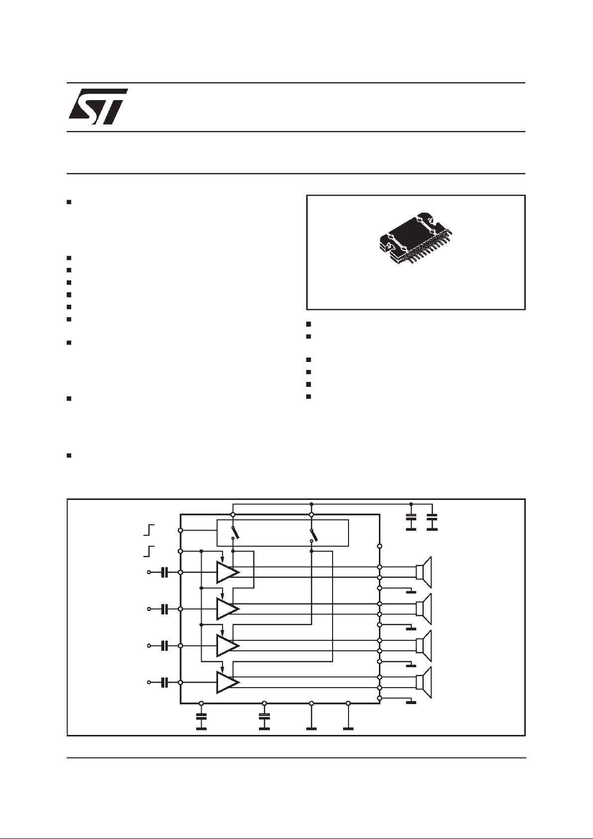
4 x 30W QUAD BRIDGE CAR RADIO AMPLIFIER
HIGHOUTPUTPOWERCAPABILITY:
4 x35W/4Ω MAX.
4 x30W/4ΩEIAJ
4 x22W/4Ω@ 14.4V, 1KHz, 10%
4 x18.5W/4Ω @ 13.2V,1KHz,10%
CLIPPINGDETECTOR
LOW DISTORTION
LOW OUTPUTNOISE
ST-BYFUNCTION
MUTEFUNCTION
AUTOMUTEAT MIN. SUPPLY VOLTAGE DE-
TECTION
DIAGNOSTICSFACILITYFOR:
– CLIPPING
– OUTTOGND SHORT
– OUTTOV
– THERMALSHUTDOWN
LOW EXTERNALCOMPONENTCOUNT:
– INTERNALLYFIXED GAIN (32dB)
– NOEXTERNALCOMPENSATION
– NOBOOTSTRAPCAPACITORS
PROTECTIONS:
OUTPUT SHORT CIRCUIT TO GND, TO V
ACROSS THE LOAD
SHORT
S
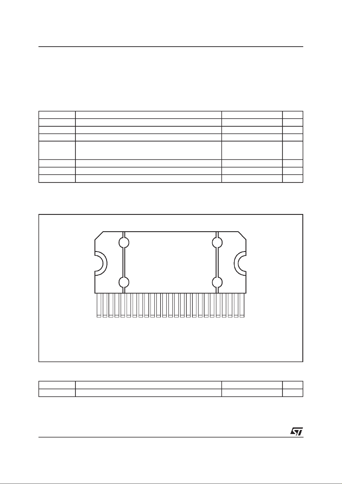
TDA7383
FLEXIWATT25
ORDERING NUMBER: TDA7383
VERYINDUCTIVE LOADS
OVERRATING CHIP TEMPERATURE WITH
SOFTTHERMAL LIMITER
LOADDUMP VOLTAGE
FORTUITOUSOPEN GND
REVERSEDBATTERY
ESD PROTECTION
DESCRIPTION
The TDA7383 is a new technology class AB
Audio Power Amplifier in Flexiwatt 25 package
designed for high end car radioapplications.
,
S
BLOCK AND APPLICATION DIAGRAM
Vcc1 Vcc2
ST-BY
MUTE
IN1
0.1µF
IN2
0.1µF
IN3
0.1µF
IN4
0.1µF
AC-GND
0.1µF47µF
October 1999
100nF2.200µF
DIAGN. OUT
OUT1+
OUT1PW-GND
OUT2+
OUT2PW-GND
OUT3+
OUT3PW-GND
OUT4+
OUT4PW-GND
SVR TAB S-GND
D93AU002C
1/12
TDA7383
DESCRIPTION(continued)
Thanks to the fully complementaryPNP/NPN output configurationthe TDA7383 allows a rail to rail
output voltage swing with no need of bootstrap
capacitors. The extremely reduced components
count allows very compact sets.
ABSOLUTE MAXIMUM RATINGS
Symbol Parameter Value Unit
V
V
CC (DC)
V
CC (pk)
CC
I
O
Operating Supply Voltage 18 V
DC Supply Voltage 28 V
Peak Supply Voltage (t = 50ms) 50 V
Output Peak Current:
Repetitive (Duty Cycle 10% at f = 10Hz)
Non Repetitive(t = 100µs)
P
tot
T
j
T
stg
Power dissipation, (T
=70°C) 80 W
case
Junction Temperature 150
Storage Temperature – 55 to150
PIN CONNECTION (Topview)
The on-board clipping detector simplifies gain
compression operations. The fault diagnostics
makes it possible to detect mistakes during CarRadioassembly and wiring in the car.
4.5
5.5
A
A
C
°
C
°
1 25
TAB
OUT2-
P-GND
ST-BY
CC
V
OUT2+
OUT1-
OUT1+
P-GND1
SVR
IN1
IN2
IN4
S-GND
IN3
OUT3+
AC-GND
OUT3-
P-GND3
CC
V
MUTE
OUT4+
D94AU117B
OUT4-
P-GND4
DIAGNOSTICS
THERMAL DATA
Symbol Parameter Value Unit
Thermal Resistance Junction to Case Max. 1
2/12
R
th j-case
C/W
°
TDA7383
ELECTRICALCHARACTERISTICS(VS= 14.4V; f = 1KHz; RL=4Ω;T
amb
=25°C;
Refer to the Testand application circuit (fig.1),unless otherwisespecified.)
Symbol Parameter Test Condition Min. Typ. Max. Unit
I
q1
V
OS
G
v
P
o
P
o EIAJ
P
o max.
THD Distortion P
e
No
SVR Supply Voltage Rejection f = 100Hz 50 65 dB
f
cl
f
ch
R
C
T
I
SB
V
SB out
V
SB IN
A
M
V
M out
V
Min
I
m (L)
I
CDOFF
I
CDON
(*) Saturated square wave output.
(**) Diagnostics output pulled-up to 5V with 10KΩ series resistor.
Quiescent Current 180 300 mA
Output Offset Voltage 200 mV
Voltage Gain 31 32 33 dB
Output Power THD = 10%
THD = 1%
THD = 10%; V
THD = 5%; V
THD = 1%; V
THD = 10%; V
THD = 1%; V
= 14V
S
= 14V
S
= 14V
S
= 13.2V
S
= 13.2V
S
20
16.5
19
17
16
17
14
22
18
21
19
17
18.5
15
EIAJ Ouput Power (*) VS = 13.7V 27.5 30 W
Max. Output Power (*) VS= 14.4V 33 35 W
= 4W 0.05 0.3 %
o
Output Noise ”A” Weighted
Bw = 20Hz to 20KHz
75
100 150
Low Cut-Off Frequency 20 Hz
High Cut-Off Frequency 75 KHz
Input Impedance 70 100 KΩ
i
Cross Talk f= 1KHz 50 70 dB
St-By Current Consumption St-By = LOW 100
St-By OUT ThresholdVoltage (Amp: ON) 3.5 V
St-By IN Threshold Voltage (Amp: OFF) 1.5 V
Mute Attenuation VO= 1Vrms 80 90 dB
Mute OUT Threshold Voltage (Amp: Play) 3.5 V
Mute IN Threshold Voltage (Amp: Mute) 1.5 V
Muting Pin Current V
MUTE
= 1.5V
51016µA
(Source Current)
Clipping Detector ”OFF” Output
THD = 1% (**) 100
Average Current
Clipping Detector ”ON” Output
THD = 10% (**) 100 240 350 µA
Average Current
W
W
W
W
W
W
W
µ
µV
µ
µ
V
A
A
3/12
TDA7383
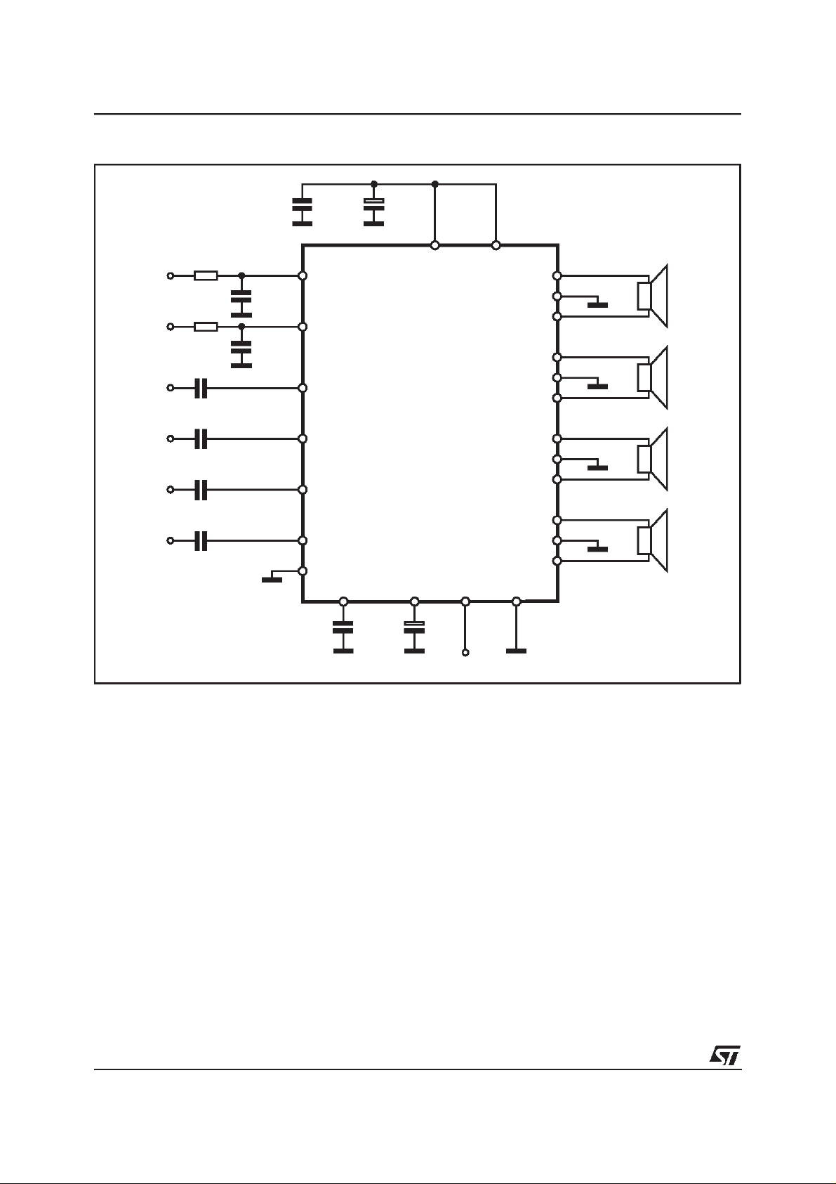
Figure 1: StandardTest and Application Circuit
ST-BY
MUTE
IN1
IN2
IN3
IN4
R1
10K
R2
47K
C1
0.1µF
C2 0.1µF
C3 0.1µF
C4 0.1µF
C9
1µF
C10
1µF
S-GND
C8
0.1µF
4
22
11
12
15
14
13
16 10 25 1
C5
0.1µF
C7
2200µF
Vcc1-2 Vcc3-4
SVR TAB
C6
47µF
620
9
8
7
5
2
3
17
18
19
21
24
23
OUT1
OUT2
OUT3
OUT4
D94AU179B
4/12
DIAGNOSTICS

Figure 2: P.C.B. and componentlayout of the figure 1 (1:1scale)
TDA7383
COMPONENTS &
TOP COPPER LAYER
TDA7383
BOTTOM COPPER LAYER
5/12

TDA7383
Figure 3: QuiescentCurrent vs. Supply Voltage
Figure 5: Output Power vs. SupplyVoltage
Figure4: Quiescent Output Voltage vs. Supply
Voltage
Figure6: Distortionvs. Output Power
THD(%)
10
Vs= 14.4V
RL = 4 Ohm
Figure 7: Distortion vs. Frequency.
THD (%)
10
Vs= 14.4 V
RL = 4 Ohm
Po= 1 W
1
0.1
1
f= 10 KHz
0.1
0
0.1 1 10
f= 1 KHz
Po(W)
Figure 8: Supply Voltage Rejection vs.
Frequency
SVR (dB)
100
Rg= 600 Ohm
90
Vripple= 1 Vrms
80
70
60
50
40
0
10 100 1000 10000
f (Hz)
6/12
30
10 100 1000 10000
f (Hz)

TDA7383
Figure 9: Output Noise vs. Source Resistance
En (µV)
200
180
Vs= 14.4 V
RL= 4 Ohm
160
140
120
22 - 22K Hz lin.
100
80
”A” wgtd
60
40
1 10 100 1k 10k 100k
Rg (Ohm)
APPLICATIONHINTS (ref.to the circuit of fig. 1)
BIASING AND SVR
As shown by fig. 11, all the TDA7383’s main sec-
tions, such as INPUTS, OUTPUTS AND AC-GND
(pin 16) are internally biased at half Supply Voltage level (Vs/2), whichis derived from the Supply
VoltageRejection (SVR) block. In this way no current flows throughthe internalfeedbacknetwork.
The AC-GND is common to all the 4 amplifiers
and represents the connection point of all the inverting inputs.
Both individual inputs and AC-GND are connected to Vs/2 (SVR) by means of 100KΩresistors.
Figure10: Power Dissipation & Efficiency vs.
OutputPower
Ptot (W)
To ensure proper operation and high supply voltage rejection, it is of fundamental importance to
provide a good impedance matching between INPUTS and AC-GROUND terminations. This impliesthat C
1,C2,C3,C4,C5
CAPACITORSHAVE
TO CARRY THE SAME NOMINAL VALUE AND
THEIR TOLERANCE SHOULDNEVER EXCEED
±10 %.
Besides its contributionto the ripple rejection, the
SVR capacitor governs the turn ON/OFFtime sequence and, consequently,plays an essential role
in the pop optimizationduring ON/OFF transients.
To conveniently serve both needs, ITS MINIMUM
RECOMMENDEDVALUE IS 10µF.
Figure 11: Input/OutputBiasing.
V
S
10KΩ
SVR AC_GND
10KΩ
100KΩ
F
0.1µ
C1 ÷ C4
100KΩ70KΩ
47µ
F
C6
IN
0.1µ
C5
F
+
-
8KΩ
400Ω
400Ω
8KΩ
-
+
TOWARDS
OTHER CHANNELS
D95AU302
7/12

TDA7383
INPUT STAGE
The TDA7383’s inputs are ground-compatibleand
can stand very high inputsignals (± 8Vpk)without
any performancesdegradation.
If the standard value for the input capacitors
(0.1µF) is adopted, the low frequency cut-off will
amount to 16 Hz.
STAND-BYAND MUTING
STAND-BY and MUTING facilities are both
CMOS-COMPATIBLE. If unused, a straight connection to Vs of theirrespective pins wouldbe admissible. Conventional low-power transistorscan
be employed to drive muting and stand-by pins in
absence of true CMOSports or microprocessors.
R-C cells have always to be used in order to
smooth down the transitions for preventing any
audible transientnoises.
Since a DC current of about 10 uA normallyflows
out of pin 22, the maximum allowable muting-series resistance (R
) is 70KΩ, which is sufficiently
2
high to permit a muting capacitor reasonably
small (about 1µF).
If R
is higher than recommended, the involved
2
risk will be that the voltage at pin 22 may rise to
above the 1.5 V threshold voltage and the device
will consequently fail to turn OFF when the mute
line is brought down.
About the stand-by, the time constant to be assigned in order to obtain a virtually pop-free transition has to be slowerthan 2.5V/ms.
tion with microprocessor-drivenaudioprocessors.
The maximum load that pin 25 can sustain is
1KΩ.
Due to its operating principles, the clipping detec-
tor has to be viewed mainly as a power-dependFigure12: Diagnosticscircuit.
25
Vpin 25
R
VREF
D95AU303A
Figure13: Clipping Detection Waveforms.
DIAGNOSTICSFACILITY
The TDA7383 is equipped with a diagnostics cir-
cuitry able to detectthe following events:
CLIPPINGin the output stage
OVERHEATING (THERMAL SHUT-DOWN
proximity)
OUTPUT MISCONNECTIONS (OUT-GND &
OUT-Vsshorts)
Diagnostics information is available across an
open collector output located at pin 25 (fig. 12)
through a current sinking whenever at least one
of the above events is recognized.
Among them, the CLIPPING DETECTOR acts in
a way to output a signal as soon as one or more
power transistorsstart being saturated.
As a result, the clipping-related signal at pin 25
takes the form of pulses, which are perfectly syncronized with each single clipping event in the
music program and reflect the same duration time
(fig. 13). Applications making use of this facility
usually operatea filtering/integrationof the pulses
train through passive R-C networks and realize a
volume (or tone bass) stepping down in associa-
8/12
ent feature rather than frequency-dependent.This
means that clipping state will be immediately signaled out whenever a fixed power level is
reached,regardlessof the audiofrequency.
In other words, this feature offers the means to
counteract the extremely sound-damaging effects
of clipping, caused by a sudden increase of odd
order harmonics and appearance of serious intermodulationphenomena.
Another possible kind of distortion control could
be the setting of a maximum allowable THD limit
(e.g. 0.5 %) over the entire audio frequency
range. Besides offering no practical advantages,
this procedure cannot be much accurate, as the
non-clipping distortion is likely to vary over frequency.
In case of OVERHEATING, pin 25 will signal out
the junction temperature proximity to the thermal
shut-down threshold. This will typically start about
o
C beforethe thermal shut-downthreshold is
2

Figure 14: DiagnosticsWaveforms.
ST-BY PIN
VOLTAGE
MUTE PIN
VOLTAGE
Vs
OUTPUT
WAVEFORM
Vpin 25
WAVEFORM
TDA7383
t
t
t
D95AU304
reached.
As variouskind of diagnostics informationis avail-
able at pin 25 (CLIPPING, SHORTS AND OVERHEATING), it may be necessary to operate some
distinctions on order to treat each event separately. This could be achieved by taking into account the intrinsically different timing of the diagnostics outputunder each circumstance.
Figure 15.
VREF
25
T1 <<
T2
VREF ≥ VREF1 >> VREF2
T1
T2
VREF1
VREF2
CLIPPING
SHORT TO GND
OR TO Vs
THERMAL
PROXIMITY
t
In fact, clipping will produce pulses normally
much shorter than thosepresent under faultyconditions. An example of circuit able to distinguish
between the two occurrences is shown by fig. 15.
STABILITYAND LAYOUT CONSIDERATIONS
If properly layouted and hooked to standard car-
radio speakers, the TDA7383 will be intrinsically
stable with no need of external compensations
-
+
-
+
CLIP DET. (TO
COMPRESSOR/
TONE CONTROL)
FAULT, THERMAL
(TO POWER SUPPLY
SECTION, µP
REGULATOR, FLASHING SYSTEM)
D95AU305A
GAIN
SHUTDOWN
VOLTAGE
9/12

TDA7383
such as output R-C cells. Dueto the high number
of channels involved, this translates into a very
remarkable components saving if compared to
similar devices on the market.
To simplify pc-board layout designs, each amplifier stage has its own power ground externallyaccessible (pins 2,8,18,24) and one supply voltage
pin foreach couple of them.
Even more important, this makes it possible to
achieve the highest possible degreeof separation
among the channels,with remarkable benefits in
termsof cross-talkand distortionfeatures.
About the layout grounding, it is particularly im-
portant to connect the AC-GND capacitor (C
)to
5
the signal GND, as close as possible to the audio
inputs ground: this will guarantee high rejection of
any common mode spurious signals.
The SVR capacitor (C
) has also to be connected
6
to the signalGND.
Supply filtering elements (C
) have naturally
7,C8
to be connected to the power-groundand located
as close as possibleto theVs pins.
Pin 1, which is mechanically attached to the device’s tab, needs to be tied to the cleanest power
ground point in the pc-board, which is generally
near the supplyfilteringcapacitors.
10/12

TDA7383
DIM.
MIN. TYP. MAX. MIN. TYP. MAX.
mm inch
A 4.45 4.50 4.65 0.175 0.177 0.183
B 1.80 1.90 2.00 0.070 0.074 0.079
C 1.40 0.055
D 0.75 0.90 1.05 0.029 0.035 0.041
E 0.37 0.39 0.42 0.014 0.015 0.016
F (1) 0.57 0.022
G 0.80 1.00 1.20 0.031 0.040 0.047
G1 23.75 24.00 24.25 0.935 0.945 0.955
H (2) 28.90 29.23 29.30 1.138 1.150 1.153
H1 17.00 0.669
H2 12.80 0.503
H3 0.80 0.031
L (2) 22.07 22.47 22.87 0.869 0.884 0.904
L1 18.57 18.97 19.37 0.731 0.747 0.762
L2 (2) 15.50 15.70 15.90 0.610 0.618 0.626
L3 7.70 7.85 7.95 0.303 0.309 0.313
L4 5 0.197
L5 3.5 0.138
M 3.70 4.00 4.30 0.145 0.157 0.169
M1 3.60 4.00 4.40 0.142 0.157 0.173
N 2.20 0.086
O 2 0.079
R 1.70 0.067
R1 0.5 0.02
R2 0.3 0.12
R3 1.25 0.049
R4 0.50 0.019
V5°(Typ.)
V1 3°(Typ.)
V2 20°(Typ.)
V3 45°(Typ.)
(1): dam-bar protusion not included
(2): molding protusionincluded
OUTLINE AND
MECHANICALDATA
Flexiwatt25
L2
H
V3
OL3 L4
V
C
H3
G
H1
G1
R3
H2
F
A
R4
N
V2
R2
R
L
L1
V1
R2
B
V
FLEX25ME
R1
L5
V1
R1 R1
E
M1
M
D
11/12

TDA7383
Information furnished is believed to be accurate and reliable. However, STMicroelectronics assumes no responsibility for the consequences
of use of such information nor for any infringement of patents or other rights of third parties which may result from its use. No license is
granted by implication or otherwise under any patent or patent rights of STMicroelectronics. Specification mentioned in this publication are
subject to change without notice. This publication supersedes and replaces all information previously supplied. STMicroelectronics products
are not authorized for use as critical components in life support devices or systems without express written approval of STMicroelectronics.
The ST logo is a registered trademark of STMicroelectronics
1999 STMicroelectronics – Printed in Italy – All Rights Reserved
STMicroelectronics GROUP OF COMPANIES
Australia - Brazil - China - Finland - France - Germany - Hong Kong - India - Italy - Japan - Malaysia - Malta - Morocco -
Singapore - Spain - Sweden - Switzerland - United Kingdom - U.S.A.
http://www.st.com
12/12
 Loading...