

Page 1
Dual bridge audio amplifier for car radio
Features
■ Minimum external component count
■ No bootstrap capacitors
■ No Boucherot cells
■ Clip detector output
■ High output power
■ Fixed gain
■ Very low stand-by current (1 µA typ)
■ No switch on/off noise
Protections
■ Output AC/DC short circuit to GND and to V
■ Very inductive loads
■ Overrating chip temperature
■ Load dump voltage
■ Fortuitous open GND
■ Reverse battery
■ ESD
Table 1. Device summary
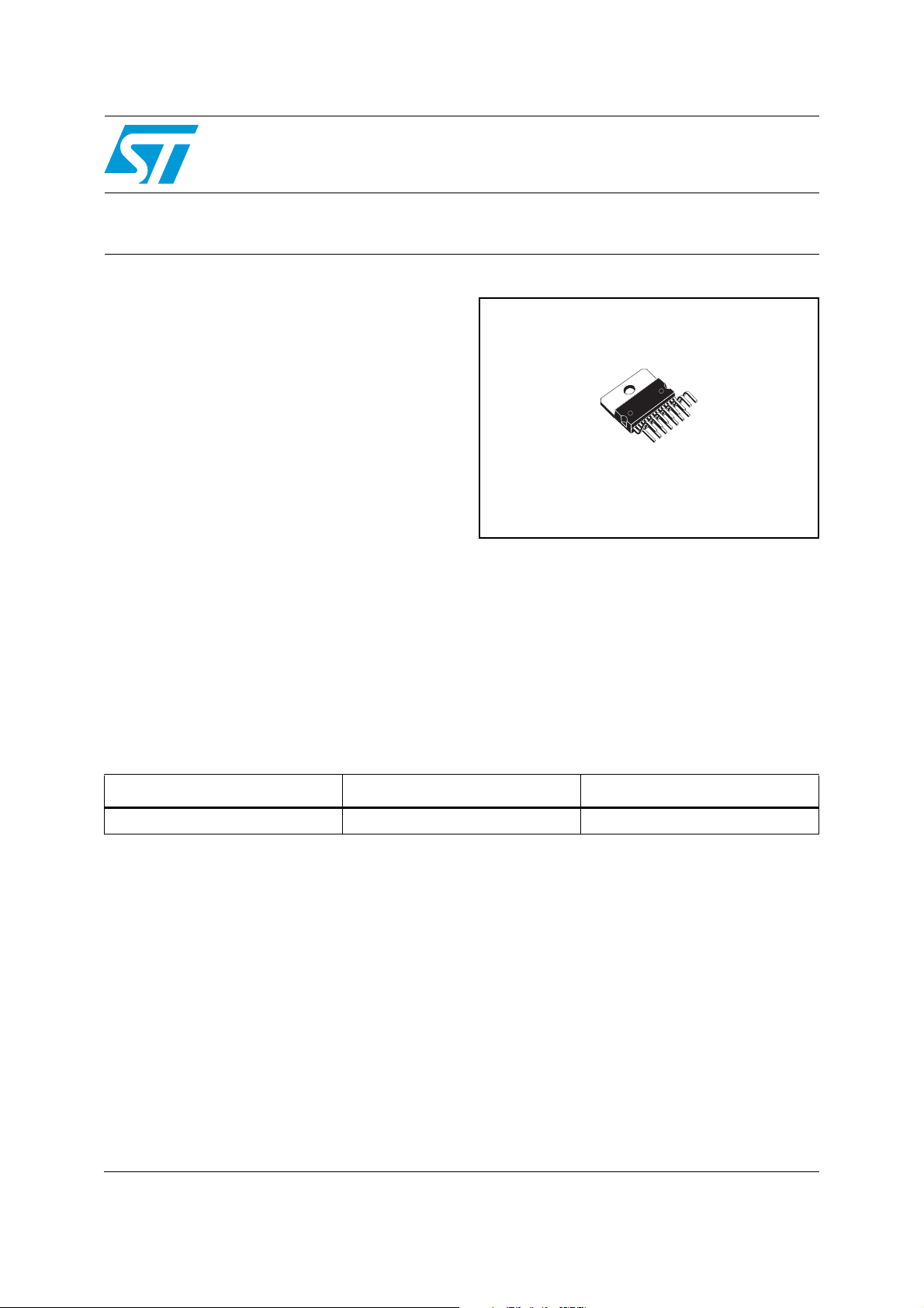
TDA7374
Multiwatt 15
S
Description
The TDA7374 is a class AB audio dual bridge
power amplifier in Multiwatt package designed for
car radio applications.
Thanks to the fully complementary PNP/NPN
output configuration the high power performances
of the TDA7374 are obtained without bootstrap
capacitors.
Order code Package Packing
TDA7374BV Multiwatt 15 Tube
June 2008 Rev 4 1/19
www.st.com
1
Page 2

Contents TDA7374
Contents
1 Block diagram and pins connections diagram . . . . . . . . . . . . . . . . . . . . 5
2 Electrical specifications . . . . . . . . . . . . . . . . . . . . . . . . . . . . . . . . . . . . . . 6
2.1 Absolute maximum ratings . . . . . . . . . . . . . . . . . . . . . . . . . . . . . . . . . . . . . 6
2.2 Thermal data . . . . . . . . . . . . . . . . . . . . . . . . . . . . . . . . . . . . . . . . . . . . . . . 6
2.3 Electrical characteristcs . . . . . . . . . . . . . . . . . . . . . . . . . . . . . . . . . . . . . . . 7
2.4 Electrical characteristics curves . . . . . . . . . . . . . . . . . . . . . . . . . . . . . . . . . 9
3 Output stage . . . . . . . . . . . . . . . . . . . . . . . . . . . . . . . . . . . . . . . . . . . . . . 11
3.1 Rail-to-rail output voltage swing with no need of bootstrap capacitors . . . 11
3.2 Absolute stability without any external compensation . . . . . . . . . . . . . . . 11
3.3 Other outstanding characteristics . . . . . . . . . . . . . . . . . . . . . . . . . . . . . . . 12
3.3.1 Clipping detector output . . . . . . . . . . . . . . . . . . . . . . . . . . . . . . . . . . . . . 12
3.3.2 Offset control . . . . . . . . . . . . . . . . . . . . . . . . . . . . . . . . . . . . . . . . . . . . . 12
3.3.3 Gain internally fixed to 26dB . . . . . . . . . . . . . . . . . . . . . . . . . . . . . . . . . 12
3.3.4 Silent turn on/off and muting/stand-by function . . . . . . . . . . . . . . . . . . . 12
3.4 Built-in protection systems . . . . . . . . . . . . . . . . . . . . . . . . . . . . . . . . . . . . 13
3.4.1 Full protection of device and loudspeakers against AC/DC short circuits
(to Gnd, to V
3.4.2 Load dump voltage surge . . . . . . . . . . . . . . . . . . . . . . . . . . . . . . . . . . . 13
3.4.3 Polarity inversion . . . . . . . . . . . . . . . . . . . . . . . . . . . . . . . . . . . . . . . . . . 13
3.4.4 Open ground . . . . . . . . . . . . . . . . . . . . . . . . . . . . . . . . . . . . . . . . . . . . . 14
3.4.5 Inductive load . . . . . . . . . . . . . . . . . . . . . . . . . . . . . . . . . . . . . . . . . . . . . 14
3.4.6 DC voltage . . . . . . . . . . . . . . . . . . . . . . . . . . . . . . . . . . . . . . . . . . . . . . . 14
3.4.7 Thermal shut-down . . . . . . . . . . . . . . . . . . . . . . . . . . . . . . . . . . . . . . . . 14
3.4.8 Loudspeaker protection . . . . . . . . . . . . . . . . . . . . . . . . . . . . . . . . . . . . . 14
, across the speakers) 13
s
3.5 Clipping detector . . . . . . . . . . . . . . . . . . . . . . . . . . . . . . . . . . . . . . . . . . . 15
3.6 What is needed for a demonstration . . . . . . . . . . . . . . . . . . . . . . . . . . . . 15
3.6.1 General Information . . . . . . . . . . . . . . . . . . . . . . . . . . . . . . . . . . . . . . . . 16
4 Package information . . . . . . . . . . . . . . . . . . . . . . . . . . . . . . . . . . . . . . . . 17
5 Revision history . . . . . . . . . . . . . . . . . . . . . . . . . . . . . . . . . . . . . . . . . . . 18
2/19
Page 3

TDA7374 List of tables
List of tables
Table 1. Device summary . . . . . . . . . . . . . . . . . . . . . . . . . . . . . . . . . . . . . . . . . . . . . . . . . . . . . . . . . . 1
Table 2. Absolute maximum ratings . . . . . . . . . . . . . . . . . . . . . . . . . . . . . . . . . . . . . . . . . . . . . . . . . . 6
Table 3. Thermal data. . . . . . . . . . . . . . . . . . . . . . . . . . . . . . . . . . . . . . . . . . . . . . . . . . . . . . . . . . . . . 6
Table 4. Electrical characteristcs . . . . . . . . . . . . . . . . . . . . . . . . . . . . . . . . . . . . . . . . . . . . . . . . . . . . 7
Table 5. Document revision history . . . . . . . . . . . . . . . . . . . . . . . . . . . . . . . . . . . . . . . . . . . . . . . . . 18
3/19
Page 4

List of figures TDA7374
List of figures
Figure 1. Block diagram . . . . . . . . . . . . . . . . . . . . . . . . . . . . . . . . . . . . . . . . . . . . . . . . . . . . . . . . . . . . 5
Figure 2. Pin connection (top view) . . . . . . . . . . . . . . . . . . . . . . . . . . . . . . . . . . . . . . . . . . . . . . . . . . . 5
Figure 3. Test and application circuit . . . . . . . . . . . . . . . . . . . . . . . . . . . . . . . . . . . . . . . . . . . . . . . . . . 8
Figure 4. Printed board and component layout of the Figure 3.. . . . . . . . . . . . . . . . . . . . . . . . . . . . . . 8
Figure 5. Quiescent drain current vs. supply voltage . . . . . . . . . . . . . . . . . . . . . . . . . . . . . . . . . . . . . . 9
Figure 6. Quiescent output voltage vs. supply voltage . . . . . . . . . . . . . . . . . . . . . . . . . . . . . . . . . . . . 9
Figure 7. Output power vs. supply voltage . . . . . . . . . . . . . . . . . . . . . . . . . . . . . . . . . . . . . . . . . . . . . . 9
Figure 8. Distortion vs. output power . . . . . . . . . . . . . . . . . . . . . . . . . . . . . . . . . . . . . . . . . . . . . . . . . . 9
Figure 9. Output power vs. frequency . . . . . . . . . . . . . . . . . . . . . . . . . . . . . . . . . . . . . . . . . . . . . . . . . 9
Figure 10. Supply volt. rejection vs. frequency for a different values of C6 capacitor . . . . . . . . . . . . . . 9
Figure 11. Cross-talk vs. frequency . . . . . . . . . . . . . . . . . . . . . . . . . . . . . . . . . . . . . . . . . . . . . . . . . . . 10
Figure 12. En input vs. Rg . . . . . . . . . . . . . . . . . . . . . . . . . . . . . . . . . . . . . . . . . . . . . . . . . . . . . . . . . . 10
Figure 13. Stand-by attenuation vs. threshold voltage. . . . . . . . . . . . . . . . . . . . . . . . . . . . . . . . . . . . . 10
Figure 14. Stand-by attenuation vs. input voltage . . . . . . . . . . . . . . . . . . . . . . . . . . . . . . . . . . . . . . . . 10
Figure 15. Clipping detector average current (pin 10) vs. distortion . . . . . . . . . . . . . . . . . . . . . . . . . . 10
Figure 16. Total power dissipation and efficiency vs. output power. . . . . . . . . . . . . . . . . . . . . . . . . . . 10
Figure 17. The new output stage . . . . . . . . . . . . . . . . . . . . . . . . . . . . . . . . . . . . . . . . . . . . . . . . . . . . . 11
Figure 18. Clipping detection waveforms. . . . . . . . . . . . . . . . . . . . . . . . . . . . . . . . . . . . . . . . . . . . . . . 12
Figure 19. A suggested LC network. . . . . . . . . . . . . . . . . . . . . . . . . . . . . . . . . . . . . . . . . . . . . . . . . . . 13
Figure 20. Voltage pulse train on pins 3 and 13 . . . . . . . . . . . . . . . . . . . . . . . . . . . . . . . . . . . . . . . . . 13
Figure 21. Maximum allowable power dissipation vs. ambient temperature . . . . . . . . . . . . . . . . . . . . 14
Figure 22. Clipping detector control routine . . . . . . . . . . . . . . . . . . . . . . . . . . . . . . . . . . . . . . . . . . . . . 15
Figure 23. Application with TDA7302 + TDA7374 . . . . . . . . . . . . . . . . . . . . . . . . . . . . . . . . . . . . . . . . 16
Figure 24. Multiwatt 15 mechanical data and package dimensions. . . . . . . . . . . . . . . . . . . . . . . . . . . 17
4/19
Page 5

TDA7374 Block diagram and pins connections diagram
1 Block diagram and pins connections diagram
Figure 1. Block diagram
Figure 2. Pin connection (top view)
5/19
Page 6
Electrical specifications TDA7374
2 Electrical specifications
2.1 Absolute maximum ratings
Table 2. Absolute maximum ratings
Symbol Parameter Value Unit
V
T
V
V
OP
PEAK
I
O
I
O
P
stg
DC supply voltage 28 V
S
Operating supply voltage 18 V
Peak supply voltage (t = 50 ms) 50 V
Output peak current (not rep. t = 100 µs) 4.5 A
Output peak current (rep. f > 10 Hz) 3.5 A
Power dissipation (T
tot
, TjStorage and junction temperature -40 to 150 °C
2.2 Thermal data
Table 3. Thermal data
Symbol Parameter Value Unit
R
th j-case
Thermal resistance junction to case max. 1.8 °C/W
= 85 °C) 36 W
case
6/19
Page 7

TDA7374 Electrical specifications
2.3 Electrical characteristcs
Table 4. Electrical characteristcs
(Refer to the test circuit; V
= 14.4 V; RL = 4 Ω, T
S
= 25 °C, f = 1 kHz, unless otherwise
amb
specified)
Symbol Parameter Test condition Min. Typ. Max. Unit
V
S
Id Total quiescent drain current 150 mA
P
O
d Distortion R
CT Cross talk
R
IN
G
V
G
V
E
IN
SVR Supply voltage rejection
ASB Stand-by attenuation 60 dB
I
SB
V
SB ON
V
SB OFF
V
OS
I
CD OFF
Supply range 8 18 V
Output power RL = 4 Ω; THD = 10 % 17 21 W
= 4 Ω; PO = 0.1 to 10 W 0.5 %
L
f = 1 kHz; R
f = 10 kHz; R
= 0 65 dB
g
= 0 55 dB
g
Input impedance 10 KΩ
Voltage gain 26 dB
Voltage gain match. 1 dB
R
= 0 to 10 kΩ; Weight A 3.5 μV
g
Input noise voltage
= 0 to 10 kΩ;
R
g
22 Hz to 22 kHz
R
= 0; f = 100 Hz 48 dB
g
= 0; f = 10 kHz 55 dB
R
g
10 μV
Stand-by current consumption 1 μA
Stand-by IN Threshold Voltage 1.5 V
Stand-by OUT threshold
voltage
3.5 V
Output offset voltage 200 mV
Clipping detector "OFF"
output average current
THD = 1 %
(1)
100 μA
I
CD ON
1. Pin 10 pulled-up to 5V with 10kΩ; RL = 4Ω
Clipping detector "ON"
output average current
THD = 10 %
7/19
(1)
190 μA
Page 8

Electrical specifications TDA7374
Figure 3. Test and application circuit
Figure 4. Printed board and component layout of the Figure 3.
8/19
Page 9

TDA7374 Electrical specifications
2.4 Electrical characteristics curves
Figure 5. Quiescent drain current vs. supply
voltage
Figure 6. Quiescent output voltage vs. supply
voltage
Figure 7. Output power vs. supply voltage Figure 8. Distortion vs. output power
Figure 9. Output power vs. frequency Figure 10. Supply volt. rejection vs. frequency
for a different values of C6 capacitor
9/19
Page 10

Electrical specifications TDA7374
Figure 11. Cross-talk vs. frequency Figure 12. En input vs. Rg
Figure 13. Stand-by attenuation vs. threshold
voltage
Figure 15. Clipping detector average current
(pin 10) vs. distortion
Figure 14. Stand-by attenuation vs. input
voltage
Figure 16. Total power dissipation and
efficiency vs. output power
10/19
Page 11

TDA7374 Output stage
3 Output stage
The fully complementary output stage was made possible by the development of a new
component: the ST exclusive power ICV PNP.
A novel design based upon the connection shown in Figure 17 has then allowed the full
exploitation of its possibilities.
Figure 17. The new output stage
The clear advantages this new approach has over classical output stages are as follows:
3.1 Rail-to-rail output voltage swing with no need of bootstrap capacitors
The output swing is limited only by the V
of 0.6 Ω each.
Classical solutions adopting composite PNP-NPN for the upper output stage have higher
saturation loss on the top side of the waveform. This unbalanced saturation causes a
significant power reduction. The only way to recover power consists of the addition of
expensive bootstrap capacitors.
of the output transistors, which are in the range
cesat
3.2 Absolute stability without any external compensation
Referring to the circuit of Figure 17 the gain V
R2/R1. The DC Output (V
By controlling the amount of this local feedback it is possible to force the loop gain (A * β) to
less than unity at frequency for which the phase shift is 180°C. This means that the output
buffer is intrinsically stable and not prone to oscillation.
Most remarkably, the above feature has been achieved in spite of the very low closed loop
gain of the amplifier.
/2) is fixed by an auxiliary amplifier common to all the channels).
CC
OUT/VIN
is greater than unity, approximately 1 +
In contrast, with the classical PNP-NPN stage, the solution adopted for reducing the gain at
high frequencies makes use of external RC networks, namely the Boucherot cells.
11/19
Page 12
Output stage TDA7374
3.3 Other outstanding characteristics
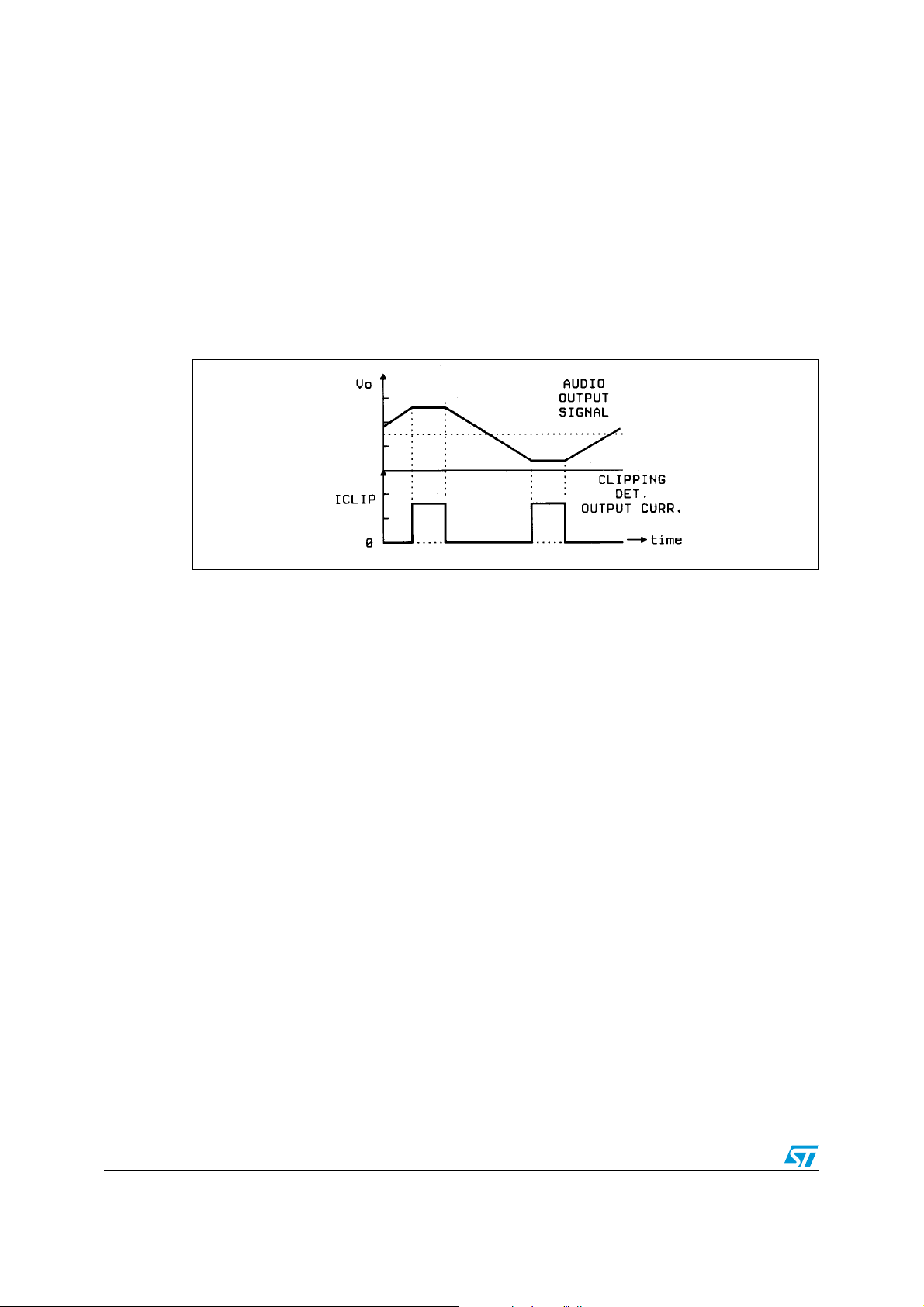
3.3.1 Clipping detector output
The TDA7374 is equipped with an internal circuit able to detect the output stage saturation
providing a proper current sinking into a open collector output (pin 10) when a certain
distortion level is reached at each output.
This particular function allows gain compression facility whenever the amplifier is
overdriven, thus obtaining high quality sound at all listening levels.
Figure 18. Clipping detection waveforms
3.3.2 Offset control
The quiescent output voltage must be as close as possible to its nominal value, so that less
undistorted power would be available.
For this reason an input bias current compensation is implemented to riduce the voltage
drop across the input resistors, which appears amplified at the outputs.
3.3.3 Gain internally fixed to 26 dB
Advantages of this design choice are in terms of:
● components and space saving
● output noise, supply voltage rejection and distortion optimization.
3.3.4 Silent turn on/off and muting/stand-by function
The stand-by can be easily activated by means of a CMOS level applied to pin 7 through a
RC filter.
Under stand-by condition the device is turned off completely (supply current = 1 µA typ.;
output attenuation = 90 dB typ.). Every ON/OFF operation is virtually pop free.
Furthermore, at turn-on the device stays in muting condition for a time determined by the
value assigned to the SVR capacitor (T= Csvr * 7,000).
While in muting the device outputs becomes insensitive to any kinds of signal that may be
present at the input terminals. In other words every transient coming from previous stages
produces no unpleasant acoustic effect to the speakers. Another situation under which the
device is totally muted is whenever the supply voltage drops lower than 7V. This is helpful to
pop suppression during the turn-off by battery switch.
12/19
Page 13

TDA7374 Output stage
3.4 Built-in protection systems
3.4.1 Full protection of device and loudspeakers against AC/DC short circuits (to Gnd, to Vs, across the speakers)
Reliable and safe operation in presence of all kinds of short circuit involving the outputs is
assured by a built-in protection system that operates in the following way:
In case of overload, a SCR is activated as soon as the current flowing through the output
transistors overcomes a preset threshold value depending on the chip temperature. The
SCR causes an interruption of the supply current of the power transistor.
3.4.2 Load dump voltage surge
The TDA7374 has a circuit which enables it to withstand a voltage pulse train on pins 3 and
13, of the type shown in Figure 20. If the supply voltage peaks to more than 50V, then an LC
filter must be inserted between the supply and pins 3 and 13, in order to assure that the
pulses at pins 3 and 13 will be held within the limits shown.
A suggested LC network is shown in Figure 19. With this network, a train of pulses with
amplitude up to 120 V and width of 2ms can be applied at point A. This type of protection is
ON when the supply voltage (pulse or DC) exceeds 18 V. For this reason the maximum
operating supply voltage is 18 V.
Figure 19. A suggested LC network
Figure 20. Voltage pulse train on pins 3 and 13
3.4.3 Polarity inversion
High current (up to 10 A) can be handled by the device with no damage for a longer period
than the blow-out time of a quick 2 A fuse (normally connected in series with the supply).
This features is added to avoid destruction, if during fitting to the car, a mistake on the
connection of the supply is made.
13/19
Page 14

Output stage TDA7374
3.4.4 Open ground
When the radio is in the ON condition and the ground is accidentally opened, a standard
audio amplifier will be damaged. On the TDA7374 protection diodes are included to avoid
any damage.
3.4.5 Inductive load
A protection diode is provided to allow use of the TDA7374 with inductive loads.
3.4.6 DC voltage
The maximum operating DC voltage for the TDA7374 is 18 V. However the device can
withstand a DC voltage up to 28 V with no damage. This could occur during winter if two
batteries are series connected to crank the engine.
3.4.7 Thermal shut-down
The presence of a thermal limiting circuit offers the following advantages:
1. an overload on the output (even if it is permanent), or an excessive ambient
temperature can be easily withstood.
2. the heatsink can have a smaller factor of safety compared with that of a conventional
circuit. There is no device damage in case of excessive junction temperature: all
happens is that P
The maximum allowable power dissipation depends upon the size of the external heatsink
(i.e. its thermal resistance); Figure 21 shows the dissipable power as a function of ambient
temperature for different thermal resistance.
(and therefore Ptot) and Id are reduced.
o
Figure 21. Maximum allowable power dissipation vs. ambient temperature
3.4.8 Loudspeaker protection
The TDA7374 guarantees safe operations even for the loudspeaker in case of accidental
shortcircuit.
Whenever a single OUT to GND, OUT to V
switched OFF so limiting dangerous DC current flowing through the loudspeaker.
short circuit occurs both the outputs are
S
14/19
Page 15

TDA7374 Output stage
3.5 Clipping detector
Figure 23 shows an application using the TDA7374 in combination with the STM
audioprocessor TDA7302. The output clipping is recognized by the microprocessor (in this
application it is simulated by a PC). The detailed way to operate of the system is
represented by the flow-chart of Figure 22.
The controller detects when the clipping is active (minimun detection width fixed by a
C29 = 12 nF external capacitor), and reduces the volume (or bass) by step of 2 dB (with a
programmable waiting time), until no more clipping is detected. Then the controller waits for
a programmable time before increasing the volume again by step of 2 dB until clipping is
again detected or the panel selected volume is reached.
Practical advantages of this application is a better sound quality deriving from operation
under no clipping conditions, which also means the availability of higher undistorted power.
Figure 22. Clipping detector control routine
3.6 What is needed for a demonstration
● IBM compatible PC with parallel port
● STM audioprocessor application disk
● TDA7302 + TDA7374 board
● Connector from audioprocessor board to PC parallel port
15/19
Page 16

Output stage TDA7374
3.6.1 General Information
In the application shown in Figure 23 the TDA7302 audioprocessor works on PC IBM
compatible.
Control is accomplished by serial bus (S-bus or I
through the PC parallel port.
The PC simulates the behaviour of the microprocessor in a real application (for example in a
car radio) and the buffer is necessary only in this application for protecting the PC.
Figure 23. Application with TDA7302 + TDA7374
2
C bus or SPI bus) sent to the test board
16/19
Page 17

TDA7374 Package information
4 Package information
In order to meet environmental requirements, ST (also) offers these devices in ECOPACK®
packages. ECOPACK® packages are lead-free. The category of second Level Interconnect
is marked on the package and on the inner box label, in compliance with JEDEC Standard
JESD97. The maximum ratings related to soldering conditions are also marked on the inner
box label.
ECOPACK is an ST trademark. ECOPACK specifications are available at: www.st.com.
Figure 24. Multiwatt 15 mechanical data and package dimensions
DIM.
A5 0.197
B 2.65 0.104
C 1.6 0.063
D 1 0.039
E 0.49 0.55 0.019 0.022
F 0.66 0.75 0.026 0.030
G 1.02 1.27 1.52 0.040 0.050 0.060
G1 17.53 17.78 18.03 0.690 0 .700 0.710
H1 19.6 0.772
H2 20.2 0.795
L 21.9 22.2 22.5 0.862 0.874 0.886
L1 21.7 22.1 22.5 0.854 0.87 0.886
L2 17.65 18.1 0.695 0.713
L3 17.25 17.5 17.75 0.679 0.689 0.699
L4 10.3 10.7 10.9 0.406 0.421 0.4 29
L7 2.65 2.9 0.104 0.114
M 4.25 4.55 4.85 0.167 0.179 0.191
M1 4.73 5.08 5.43 0.186 0.200 0.214
S 1.9 2.6 0.075 0.102
S1 1.9 2.6 0.075 0.102
Dia1 3.65 3.85 0.144 0.152
mm inch
MIN. TYP. MAX. MIN. TYP. MAX.
OUTLINE AND
MECHANICAL DATA
Multiwatt15 (Vertical)
0016036 J
17/19
Page 18

Revision history TDA7374
5 Revision history
Table 5. Document revision history
Date Revision Changes
12-Oct-1999 3 Initial release.
Document reformatted.
30-Jun-2008 4
Added Table 1: Device summary.
Added ECOPACK description in Section 4: Package information.
18/19
Page 19

TDA7374
Please Read Carefully:
Information in this document is provided solely in connection with ST products. STMicroelectronics NV and its subsidiaries (“ST”) reserve the
right to make changes, corrections, modifications or improvements, to this document, and the products and services described herein at any
time, without notice.
All ST products are sold pursuant to ST’s terms and conditions of sale.
Purchasers are solely responsible for the choice, selection and use of the ST products and services described herein, and ST assumes no
liability whatsoever relating to the choice, selection or use of the ST products and services described herein.
No license, express or implied, by estoppel or otherwise, to any intellectual property rights is granted under this document. If any part of this
document refers to any third party products or services it shall not be deemed a license grant by ST for the use of such third party products
or services, or any intellectual property contained therein or considered as a warranty covering the use in any manner whatsoever of such
third party products or services or any intellectual property contained therein.
UNLESS OTHERWISE SET FORTH IN ST’S TERMS AND CONDITIONS OF SALE ST DISCLAIMS ANY EXPRESS OR IMPLIED
WARRANTY WITH RESPECT TO THE USE AND/OR SALE OF ST PRODUCTS INCLUDING WITHOUT LIMITATION IMPLIED
WARRANTIES OF MERCHANTABILITY, FITNESS FOR A PARTICULAR PURPOSE (AND THEIR EQUIVALENTS UNDER THE LAWS
OF ANY JURISDICTION), OR INFRINGEMENT OF ANY PATENT, COPYRIGHT OR OTHER INTELLECTUAL PROPERTY RIGHT.
UNLESS EXPRESSLY APPROVED IN WRITING BY AN AUTHORIZED ST REPRESENTATIVE, ST PRODUCTS ARE NOT
RECOMMENDED, AUTHORIZED OR WARRANTED FOR USE IN MILITARY, AIR CRAFT, SPACE, LIFE SAVING, OR LIFE SUSTAINING
APPLICATIONS, NOR IN PRODUCTS OR SYSTEMS WHERE FAILURE OR MALFUNCTION MAY RESULT IN PERSONAL INJURY,
DEATH, OR SEVERE PROPERTY OR ENVIRONMENTAL DAMAGE. ST PRODUCTS WHICH ARE NOT SPECIFIED AS "AUTOMOTIVE
GRADE" MAY ONLY BE USED IN AUTOMOTIVE APPLICATIONS AT USER’S OWN RISK.
Resale of ST products with provisions different from the statements and/or technical features set forth in this document shall immediately void
any warranty granted by ST for the ST product or service described herein and shall not create or extend in any manner whatsoever, any
liability of ST.
ST and the ST logo are trademarks or registered trademarks of ST in various countries.
Information in this document supersedes and replaces all information previously supplied.
The ST logo is a registered trademark of STMicroelectronics. All other names are the property of their respective owners.
© 2008 STMicroelectronics - All rights reserved
STMicroelectronics group of companies
Australia - Belgium - Brazil - Canada - China - Czech Republic - Finland - France - Germany - Hong Kong - India - Israel - Italy - Japan -
Malaysia - Malta - Morocco - Singapore - Spain - Sweden - Switzerland - United Kingdom - United States of America
www.st.com
19/19
 Loading...