

Page 1

Features
■ Input multiplexer
– Two stereo and one mono inputs
– One quasi differential input
– Selectable input gain for optimal adaptation
to different sources
■ Fully programmable loudness function
■ Volume control in 0.3dB steps including gain
up to 20dB
■ Zero crossing mute, soft mute and direct mute
■ Bass and treble control
■ Four speaker attenuators
– Four independent speakers control in
1.25dB steps for balance and fader facilities
– Independent mute function
■ All functions programmable via serial I
2
C bus
Description
The audioprocessor TDA7342 is an upgrade of
the TDA731X audioprocessor family.
TDA7342
Digitally controlled audio processor
LQFP32
Due to a highly linear signal processing, using
CMOS-switching techniques instead of standard
bipolar multipliers, very low distortion and very
low noise are obtained. Several new features like
softmute, and zero-crossing mute are
implemented. The soft Mute function can be
activated in two ways:
1. Via serial bus (Mute byte, bit D0)
2. Directly on pin 21 through an I/O line of the
microcontroller
Very low DC stepping is obtained by use of a
BICMOS technology.
Order codes
Part number Package Packing
TDA7342N LQFP32 Tube
TDA7342NTR LQFP32 Tape and reel
November 2006 Rev 2 1/20
www.st.com
1
Page 2

Contents TDA7342
Contents
1 Block diagram and pin descriptions . . . . . . . . . . . . . . . . . . . . . . . . . . . . 5
1.1 Block diagram . . . . . . . . . . . . . . . . . . . . . . . . . . . . . . . . . . . . . . . . . . . . . . . 5
1.2 Pin description . . . . . . . . . . . . . . . . . . . . . . . . . . . . . . . . . . . . . . . . . . . . . . 5
2 Electrical specifications . . . . . . . . . . . . . . . . . . . . . . . . . . . . . . . . . . . . . . 6
2.1 Absolute maximum ratings . . . . . . . . . . . . . . . . . . . . . . . . . . . . . . . . . . . . . 6
3 I2C Bus interface . . . . . . . . . . . . . . . . . . . . . . . . . . . . . . . . . . . . . . . . . . . 10
3.1 Data validity . . . . . . . . . . . . . . . . . . . . . . . . . . . . . . . . . . . . . . . . . . . . . . . 10
3.2 Start and stop conditions . . . . . . . . . . . . . . . . . . . . . . . . . . . . . . . . . . . . . 10
3.3 Byte format . . . . . . . . . . . . . . . . . . . . . . . . . . . . . . . . . . . . . . . . . . . . . . . . 10
3.4 Acknowledge . . . . . . . . . . . . . . . . . . . . . . . . . . . . . . . . . . . . . . . . . . . . . . 10
3.5 Transmission without acknowledge . . . . . . . . . . . . . . . . . . . . . . . . . . . . . 10
4 Software specification . . . . . . . . . . . . . . . . . . . . . . . . . . . . . . . . . . . . . . 12
4.1 Interface protocol . . . . . . . . . . . . . . . . . . . . . . . . . . . . . . . . . . . . . . . . . . . 12
4.2 Auto increment . . . . . . . . . . . . . . . . . . . . . . . . . . . . . . . . . . . . . . . . . . . . . 12
4.3 Transmitted data . . . . . . . . . . . . . . . . . . . . . . . . . . . . . . . . . . . . . . . . . . . . 13
4.4 Data byte specification . . . . . . . . . . . . . . . . . . . . . . . . . . . . . . . . . . . . . . . 13
5 Package information . . . . . . . . . . . . . . . . . . . . . . . . . . . . . . . . . . . . . . . . 18
6 Revision history . . . . . . . . . . . . . . . . . . . . . . . . . . . . . . . . . . . . . . . . . . . 19
2/20
Page 3

TDA7342 List of tables
List of tables
Table 1. Absolute maximum ratings . . . . . . . . . . . . . . . . . . . . . . . . . . . . . . . . . . . . . . . . . . . . . . . . . . 6
Table 2. Thermal data. . . . . . . . . . . . . . . . . . . . . . . . . . . . . . . . . . . . . . . . . . . . . . . . . . . . . . . . . . . . . 6
Table 3. Quick reference data . . . . . . . . . . . . . . . . . . . . . . . . . . . . . . . . . . . . . . . . . . . . . . . . . . . . . . 6
Table 4. Electrical characteristics . . . . . . . . . . . . . . . . . . . . . . . . . . . . . . . . . . . . . . . . . . . . . . . . . . . . 6
Table 5. Subaddress (receive mode) . . . . . . . . . . . . . . . . . . . . . . . . . . . . . . . . . . . . . . . . . . . . . . . . 12
Table 6. Send mode . . . . . . . . . . . . . . . . . . . . . . . . . . . . . . . . . . . . . . . . . . . . . . . . . . . . . . . . . . . . . 13
Table 7. Input selector . . . . . . . . . . . . . . . . . . . . . . . . . . . . . . . . . . . . . . . . . . . . . . . . . . . . . . . . . . . 13
Table 8. Loudness . . . . . . . . . . . . . . . . . . . . . . . . . . . . . . . . . . . . . . . . . . . . . . . . . . . . . . . . . . . . . . 14
Table 9. Mute . . . . . . . . . . . . . . . . . . . . . . . . . . . . . . . . . . . . . . . . . . . . . . . . . . . . . . . . . . . . . . . . . . 14
Table 10. Speaker attenuators (LF, LR, RF, RR) . . . . . . . . . . . . . . . . . . . . . . . . . . . . . . . . . . . . . . . . 15
Table 11. Bass/Treble. . . . . . . . . . . . . . . . . . . . . . . . . . . . . . . . . . . . . . . . . . . . . . . . . . . . . . . . . . . . . 15
Table 12. Volume . . . . . . . . . . . . . . . . . . . . . . . . . . . . . . . . . . . . . . . . . . . . . . . . . . . . . . . . . . . . . . . . 17
Table 13. Document revision history . . . . . . . . . . . . . . . . . . . . . . . . . . . . . . . . . . . . . . . . . . . . . . . . . 19
3/20
Page 4

List of figures TDA7342
List of figures
Figure 1. Block diagram . . . . . . . . . . . . . . . . . . . . . . . . . . . . . . . . . . . . . . . . . . . . . . . . . . . . . . . . . . . . 5
Figure 2. Pin connections (Top view). . . . . . . . . . . . . . . . . . . . . . . . . . . . . . . . . . . . . . . . . . . . . . . . . . 5
Figure 3. Data validity on the I2C BUS . . . . . . . . . . . . . . . . . . . . . . . . . . . . . . . . . . . . . . . . . . . . . . . 11
Figure 4. Timing diagram of I2C BUS . . . . . . . . . . . . . . . . . . . . . . . . . . . . . . . . . . . . . . . . . . . . . . . . 11
Figure 5. Acknowledge on the I2C BUS . . . . . . . . . . . . . . . . . . . . . . . . . . . . . . . . . . . . . . . . . . . . . . 11
Figure 6. Interface protocol . . . . . . . . . . . . . . . . . . . . . . . . . . . . . . . . . . . . . . . . . . . . . . . . . . . . . . . . 12
Figure 7. LQFP32 Mechanical data & package dimensions . . . . . . . . . . . . . . . . . . . . . . . . . . . . . . . 18
4/20
Page 5
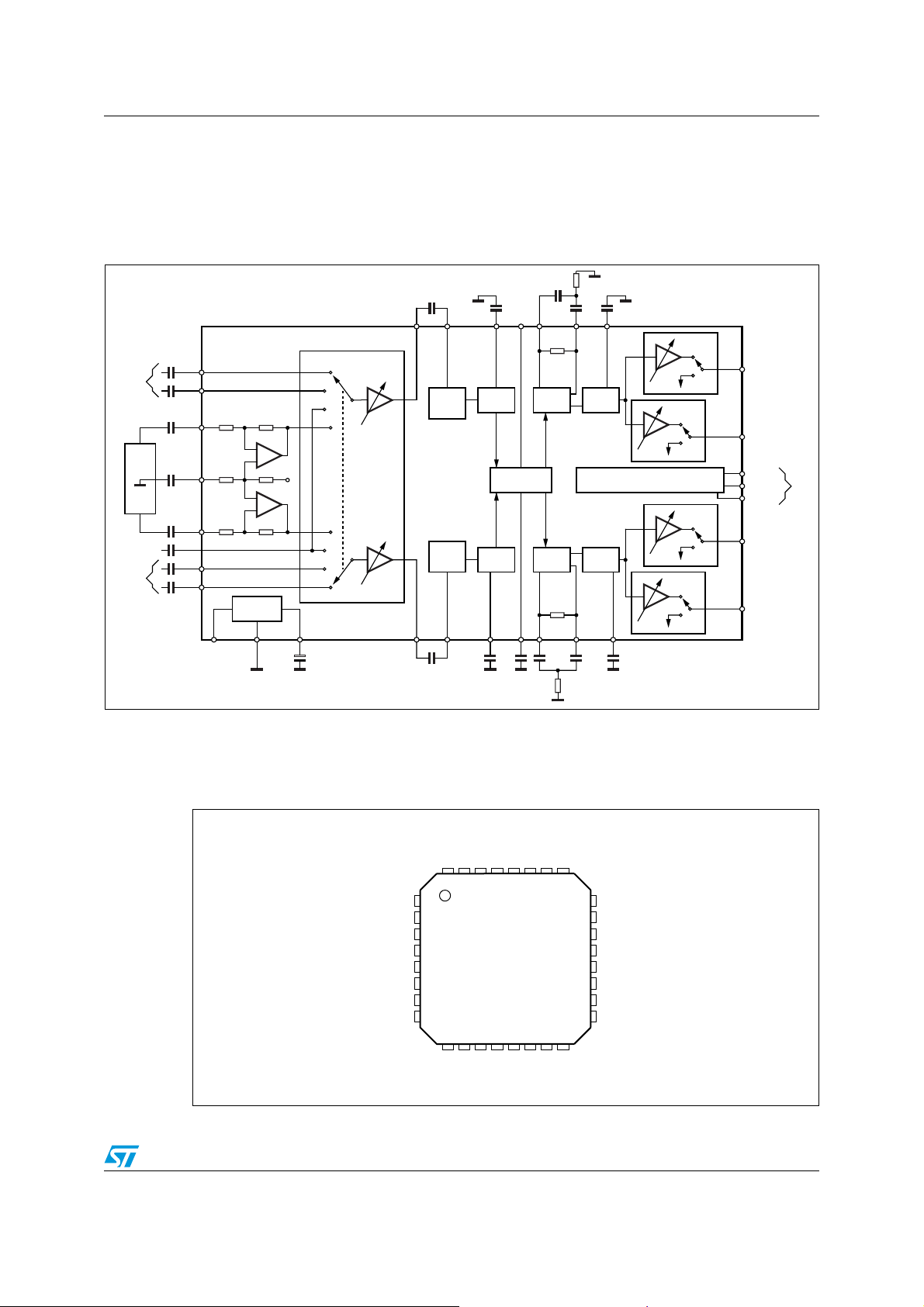
TDA7342 Block diagram and pin descriptions
1 Block diagram and pin descriptions
1.1 Block diagram
Figure 1. Block diagram
LEFT
INPUTS
CD
MONO INPUT
RIGHT
INPUTS
C8
C4
C1
C2
C6
CD GND
C3
C7
C5
13
L1
12
L2
11
L3
10
5
R3
M
8
R2
6
R1
7
V
S
SUPPLY
30 31 29
L1
L2
M
L3
R3
M
R2
R1
10μF C9
INPUT
SELECTOR
+ GAIN
VOL
VOL
CSMOUT(R)CREF
CSM
47nF
21
SM
SOFT
MUTE
C17 100nF
BOUT(L)
18 17
20 19 1
C11
ZERO
CROSS +
MUTE
ZERO
CROSS +
MUTE
2 4
IN(R)
C10
C13 47nF
LOUD(L)
LOUD(R)
C12
47nF
9
LOUD+
LOUD+
OUT(L) IN(L)
16 15
314
R2
4.7K
100nF
BIN(L)
32
BASS
TREBLE
SERIAL BUS DECODER + LATCHES
BASS
TREBLE
BOUT(R) BIN(R)
C14
C15
100nF
100nF
4.7K
R1
C19 2.7nFC18
TREBLE(L)
TREBLE(R)
C16
2.7nF
SPKR
ATT
MUTE
SPKR
ATT
MUTE
SPKR
ATT
MUTE
SPKR
ATT
MUTE
25
23
28
27
26
24
22
D94AU104B
OUT
LEFT FRONT
OUT
LEFT REAR
SCL
SDA
DIGGND
OUT
RIGHT FRONT
OUT
RIGHT REAR
BUS
1.2 Pin description
Figure 2. Pin connections (Top view)
TR R
IN R
OUT R
LOUD R
IN R3
IN R2
IN R1
MONO
S
GND
TR L
V
CREF
SCL
SDA
DIG GND
OUT LF
323031 29 28 27 26 25
1
2
3
4
5
6
7
8
11 12 13 14 15 16
910
IN L3
LOUD L
CD GND
IN L2
IN L1
CSM
IN L
24
23
22
21
20
19
18
17
OUT L
OUT RF
OUT LR
OUT RR
SM
BOUT R
BIN R
BOUT L
BIN L
D94AU105A
5/20
Page 6
Electrical specifications TDA7342
2 Electrical specifications
2.1 Absolute maximum ratings
Table 1. Absolute maximum ratings
Symbol Parameter Value Unit
V
Operating supply voltage 10.5 V
S
T
amb
T
Table 2. Thermal data
Symbol Parameter Value Unit
Operating ambient temperature -40 to 85 °C
Storage temperature range -55 to 150 °C
stg
R
th j-amb
Table 3. Quick reference data
Thermal resistance junction-pins 150 °C/W
Symbol Parameter Min. Typ. Max. Unit
Supply voltage 6 9 10.2 V
V
S
V
Max. input signal handling 2.1 2.6 Vrms
CL
THD Total harmonic distortion V = 1Vrms f = 1KHz 0.01 0.08 %
S/N Signal to noise ratio 106 dB
Channel separation 100 dB
S
C
Volume control 0.3dB step -59.7 20 dB
Treble control 2dB step -14 +14 dB
Bass control 2dB step -10 +18 dB
Fader and balance control 1.25dB step -38.75 0 dB
Input gain 3.75dB step 0 11.25 dB
Mute attenuation 100 dB
Table 4. Electrical characteristics
(V
= 9V; RL = 10KΩ; Rg = 50Ω; T
S
= 25°C; all gains = 0dB; f = 1KHz. Refer
amb
to the test circuit, unless otherwise specified.)
Symbol Parameter Test condition Min. Typ. Max. Unit
Input selector
R
Input resistance 70 100 130 KΩ
I
Clipping level d ≤ 0.3% 2.1 2.6 V
V
CL
S
Input separation 80 100 dB
I
Output load resistance 2 KΩ
R
L
Minimum input gain -0.75 0 0.75 dB
G
I MIN
G
Maximum input gain 10.25 11.25 12.25 dB
I MAX
6/20
RMS
Page 7

TDA7342 Electrical specifications
Table 4. Electrical characteristics (continued)
(V
= 9V; RL = 10KΩ; Rg = 50Ω; T
S
= 25°C; all gains = 0dB; f = 1KHz. Refer
amb
to the test circuit, unless otherwise specified.)
Symbol Parameter Test condition Min. Typ. Max. Unit
Step resolution 2.75 3.75 4.75 dB
G
step
e
Input noise 20Hz to 20 KHz unweighted 2.3 μV
N
V
DC
DC Steps
Differential input (IN 3)
Adjacent gain steps 1.5 10 mV
G
IIN
to G
3 mV
IMAX
Input selector BIT D6 = 0
(0dB)
R
Input resistance
I
Input selector BIT D6 = 1(6dB)
= 1V
V
CMRR
Common mode rejection
ratio
CM
f = 10KHz 45 70 dB
d Distortion VI= 1V
e
Input noise 20Hz to 20KHz; Flat; D6 = 0 5 μV
IN
; f =1KHz 48 75 dB
RMS
RMS
10 15 20 KΩ
14 20 30 KΩ
0.01 0.08 %
D6 = 0 -1 0 1 dB
G
Differential gain
DIFF
D6 = 1 -7 -6 -5 dB
Volume control
Input resistance 35 50 KΩ
R
I
G
Maximum gain 18.75 20 21.25 dB
MAX
A
A
STEPC
A
STEPF
MAX
Maximum attenuation 57.7 59.7 62.7 dB
Step resolution coarse
attenuation
Step resolution fine
attenuation
0.5 1.25 2.0 dB
0.11 0.31 0.51 dB
G = 20 to -20dB -1.25 0 1.25 dB
E
Attenuation set error
A
Tracking error 2 dB
E
t
G = -20 to -58dB -3 2 dB
Adjacent attenuation Steps -3 0 3 mV
V
DC Steps
DC
From 0dB to A
0.5 5 mV
MAX
Loudness control
RI Internal resistor Loud = On 35 50 65 KΩ
A
A
MAX
Maximum attenuation 17.5 18.75 20.0 dB
Step resolution 0.5 1.25 2.0 dB
step
Zero crossing mute
7/20
Page 8

Electrical specifications TDA7342
Table 4. Electrical characteristics (continued)
(V
= 9V; RL = 10KΩ; Rg = 50Ω; T
S
= 25°C; all gains = 0dB; f = 1KHz. Refer
amb
to the test circuit, unless otherwise specified.)
Symbol Parameter Test condition Min. Typ. Max. Unit
WIN = 11 20 mV
V
Zero crossing threshold
TH
(1)
WIN = 10 40 mV
WIN = 01 80 mV
WIN = 00 160 mV
A
MUTE
V
Mute attenuation 80 100 dB
DC Step 0dB to Mute 0 3 mV
DC
Soft mute
A
Mute attenuation 45 60 dB
MUTE
C
= 22nF; 0 to -20dB; I =
CSM
I
T
ON Delay time
DON
OFF current
T
DOFF
V
THSM
R
V
V
SMH
Soft mute threshold 1.5 2.5 3.5 V
Pull-up resistor (pin 21)
INT
(pin 21) Level high 3.5 V
(pin 21) Level low Soft mute active 1 V
SML
MAX
= 22nF; 0 to -20dB; I =
C
CSM
I
MIN
V
= 0V; I = I
V
(2)
CSM
CSM
= 0V; I = I
MAX
MIN
0.7 1 1.7 ms
20 35 55 ms
25 50 75 μA
1 μA
35 50 65 KΩ
Bass control
B
BOOST
B
A
Rg
Max bass boost 15 18 20 dB
Max bass cut -8.5 -10 -11.5 dB
CUT
Step Resolution 1 2 3 dB
step
Internal Feedback
Resistance
Treble control
C
RANGE
A
Control Range ±13 ±14 ±15 dB
Step Resolution 1 2 3 dB
step
Speaker attenuators
C
RANGE
A
A
MUTE
E
V
Control range 35 37.5 40 dB
Step resolution 0.5 1.25 2.00 dB
step
Output mute attenuation Data word = XXX11111 80 100 dB
Attenuation set error 1.25 dB
A
DC Steps Adjacent attenuation steps 0 3 mV
DC
8/20
45 65 85 KΩ
Page 9

TDA7342 Electrical specifications
Table 4. Electrical characteristics (continued)
(V
= 9V; RL = 10KΩ; Rg = 50Ω; T
S
= 25°C; all gains = 0dB; f = 1KHz. Refer
amb
to the test circuit, unless otherwise specified.)
Symbol Parameter Test condition Min. Typ. Max. Unit
Audio output
V
R
R
V
Clipping Level d = 0.3% 2.1 2.6 Vrms
clip
Output Load Resistance 2 KΩ
L
Output Impedance 30 100 Ω
O
DC Voltage Level 3.5 3.8 4.1 V
DC
General
V
I
Supply Voltage 6 9 10.2 V
CC
Supply Current 5 10 15 mA
CC
f = 1KHz 60 80 dB
PSRR
e
S/N Signal to Noise Ratio All Gains = 0dB; V
S
Power Supply Rejection
Ratio
Output Noise
NO
Total Tracking Error
E
t
Channel Separation 80 100 dB
C
d Distortion V
B = 20 to 20kHz "A"
weighted
Output muted (B = 20 to
20kHz flat)
All gains 0dB (B = 20 to
20kHz flat)
A
= 0 to -20dB 0 1 dB
V
= -20 to -60dB 0 2 dB
A
V
= 1Vrms 106 dB
O
=1V 0.01 0.08 %
IN
65 dB
2.5 μV
5 15 μV
Bus inputs
V
V
I
V
1. WIN represents the MUTE programming bit pair D6, D5 for the zero crossing window threshold
2. Internal pull-up resistor to Vs/2; LOW = softmute active
Input Low Voltage 1 V
IL
Input High Voltage 3 V
lN
Input Current VIN = 0.4V -5 5 μA
lN
Output Voltage SDA
O
Acknowledge
IO= 1.6mA 0.4 0.8 V
9/20
Page 10

I2C Bus interface TDA7342
3 I2C Bus interface
Data transmission from the microprocessor to the TDA7342 and vice versa takes place
through the 2 wires of the I
up resistors to the positive supply voltage must be externally connected).
2
C BUS interface, consisting of the two lines SDA and SCL (pull-
3.1 Data validity
As shown in fig. 4, the data on the SDA line must be stable during the high period of the
clock. The HIGH and LOW state of the data line can only change when the clock signal on
the SCL line is LOW.
3.2 Start and stop conditions
As shown in fig. 5 a start condition is a HIGH to LOW transition of the SDA line while SCL is
HIGH. The stop condition is a LOW to HIGH transition of the SDA line while SCL is HIGH.
A STOP condition must be sent before each START condition.
3.3 Byte format
Every byte transferred to the SDA line must contain 8 bits. Each byte must be followed by
an acknowledge bit. The MSB is transferred first.
3.4 Acknowledge
The master (microprocessor) puts a resistive HIGH level on the SDA line during the
acknowledge clock pulse (see
fig. 6). The peripheral (audioprocessor) that acknowledges has to pull-down (LOW) the SDA
line during the acknowledge clock pulse, so that the SDA line is stable LOW during this
clock pulse.
The audioprocessor which has been addressed has to generate an acknowledgment after
the reception of each byte, otherwise the SDA line remains at the HIGH level during the
ninth clock pulse time. In this case the master transmitter can generate the STOP
information in order to abort the transfer.
3.5 Transmission without acknowledge
Avoiding to detect the acknowledge of the audioprocessor, the microprocessor can use a
simpler transmission: simply it waits one clock without checking the slave acknowledging,
and sends the new data. This approach of course is less protected from misworking and
decreases the noise immunity.
10/20
Page 11

TDA7342 I2C Bus interface
Figure 3. Data validity on the I2C BUS
SDA
SCL
STABLE, DATA
Figure 4. Timing diagram of I
SCL
SDA
DATA LINE
VALID
2
C BUS
CHANGE
DATA
ALLOWED
D99AU1031
2
I
CBUS
START
Figure 5. Acknowledge on the I
SCL
SDA
START
1
MSB
D99AU1032
2
C BUS
23789
D99AU1033
STOP
ACKNOWLEDGMENT
FROM RECEIVER
11/20
Page 12

Software specification TDA7342
4 Software specification
4.1 Interface protocol
The interface protocol comprises:
● A start condition (s)
● A chip address byte, (the LSB bit determines read/write transmission)
● A subaddress byte.
● A sequence of data (N-bytes + acknowledge)
● A stop condition (P)
Figure 6. Interface protocol
CHIP ADDRESS
MSB
S 1 0 0 0 1 0 0 R/W
D05AU1575
ACK = Acknowledge
S = Start
P = Stop
I = Auto Increment
X = Not used
Max clock speed 500kbits/s
4.2 Auto increment
If bit I in the subaddress byte is set to "1", the auto increment of the subaddress is enabled
Table 5. Subaddress (receive mode)
MSB LSB Function
X X X I A3 A2 A1 A0
LSB
SUBADDRESS DATA 1 ... DATA n
MSB LSB MSB LSB
XXX A3A2A1A
ACK
I ACK DATA ACK P
0
0 0 0 0 Input selector
0 0 0 1 Loudness
0 0 1 0 Volume
0 0 1 1 Bass, treble
0 1 0 0 Speaker attenuator LF
0 1 0 1 Speaker attenuator LR
0 1 1 0 Speaker attenuator RF
0 1 1 1 Speaker attenuator RR
1 0 0 0 Mute
12/20
Page 13

TDA7342 Software specification
4.3 Transmitted data
Table 6. Send mode
MSB LSB
X X X X X SM ZM X
ZM = Zero crossing muted (HIGH active)
SM = Soft mute activated (HIGH active)
X = Not used
The transmitted data is automatically updated after each ACK.
Transmission can be repeated without new chip address.
4.4 Data byte specification
X = not relevant; set to "1" during testing
Table 7. Input selector
MSB LSB
Function
D7 D6
D5 D4 D3 D2 D1 D0
0 1 0 0 0 not used
0 1 0 0 1 IN 2
0 1 0 1 0 IN 1
0 1 0 1 1 AM mono
0 1 1 0 0 not used
0 1 1 0 1 not used
0 1 1 1 0 not allowed
0 1 1 1 1 not allowed
0 1 0 0 11.25dB gain
0 1 0 1 7.5dB gain
0 1 1 0 3.75dB gain
0 1 1 1 0dB gain
0
1
0dB differential input gain
(IN3)
-6dB differential input
gain (IN3)
For example to select the IN 2 input with a gain of 7.5dB the Data Byte is: X X 1 0 1 0 0 1
13/20
Page 14

Software specification TDA7342
Table 8. Loudness
MSB LSB
Function
D7 D6
X X X 0 0 0 0 0 0dB
X X X 0 0 0 0 1 -1.25dB
X X X 0 0 0 1 0 -2.5dB
X X X 0 0 0 1 1 -3.75dB
X X X 0 0 1 0 0 -5dB
X X X 0 0 1 0 1 -6.25dB
X X X 0 0 1 1 0 -7.5dB
X X X 0 0 1 1 1 -8.75dB
X X X 0 1 0 0 0 -10dB
X X X 0 1 0 0 1 -11.25dB
X X X 0 1 0 1 0 -12.5dB
X X X 0 1 0 1 1 -13.75dB
X X X 0 1 1 0 0 -15dB
X X X 0 1 1 0 1 -16.25dB
D5 D4 D3 D2 D1 D0
X X X 0 1 1 1 0 -17.5dB
X X X 0 1 1 1 1 -18.75dB
X X X 1 D3 D2 D1 D0 Loudness OFF (1)
For example to select -17.5dB attenuation, loudness OFF, the Data Byte is: X X X1 1 1 1 0
NOTE 1: If the loudness is switched OFF, the loudness stage is acting like a volume attenuator with flat
frequency response. D0 to D3 determine the attenuation level.
Table 9. Mute
MSB LSB
Function
D7 D6
D5 D4 D3 D2 D1 D0
1 Soft mute on
0 1 Soft mute with fast slope (I = I
1 1 Soft mute with slow slope (I = I
MAX
MIN
)
)
1 Direct mute
0 1 Zero crossing mute on
0 0
1
Zero crossing mute off
(delayed until the next zerocrossing)
Zero crossing mute and pause detector
reset
0 0 160mV ZC Window threshold (WIN = 00)
0 1 80mV ZC Window threshold (WIN = 01)
14/20
Page 15

TDA7342 Software specification
Table 9. Mute
MSB LSB
Function
D7 D6
D5 D4 D3 D2 D1 D0
1 0 40mV ZC Window threshold (WIN = 10)
1 1 20mV ZC Window threshold (WIN = 11)
0 Non symmetrical bass cut (note 4)
1 Symmetrical bass cut
An additional direct mute function is included in the speaker attenuators.
Note 4: Bass cut for very low frequencies; should not be used at +16 and +18dB bass boost (DC gain)
Table 10. Speaker attenuators (LF, LR, RF, RR)
MSB LSB
Function
D7 D6
X X X 0 0 0 0dB
X X X 0 0 1 -1.25dB
X X X 0 1 0 -2.5dB
D5 D4 D3 D2 D1 D0
1.25dB step
X X X 0 1 1 -3.75dB
X X X 1 0 0 -5dB
X X X 1 0 1 -6.25dB
X X X 1 1 0 -7.5dB
X X X 1 1 1 -8.75dB
10dB step
X X X 0 0 0dB
X X X 0 1 -10dB
X X X 1 0 -20dB
X X X 1 1 -30dB
X X X 1 1 1 1 1 Speaker mute
For example an attenuation of 25dB on a selected output is given by: X X X1 0 1 0 0
Table 11. Bass/Treble
MSB LSB
Function
D7 D6
Treble step
0 0 0 0 -14dB
D5 D4 D3 D2 D1 D0
0 0 0 1 -12dB
15/20
Page 16

Software specification TDA7342
Table 11. Bass/Treble (continued)
MSB LSB
Function
D7 D6
0 0 1 0 -10dB
0 0 1 1 -8dB
0 1 0 0 -6dB
0 1 0 1 -4dB
0 1 1 0 -2dB
0 1 1 1 0dB
1 1 1 1 0dB
1 1 1 0 2dB
1 1 0 1 4dB
1 1 0 0 6dB
1 0 1 1 8dB
1 0 1 0 10dB
D5 D4 D3 D2 D1 D0
1 0 0 1 12dB
1 0 0 0 14dB
Bass steps
0 0 1 0 -10dB
0 0 1 1 -8dB
0 1 0 0 -6dB
0 1 0 1 -4dB
0 1 1 0 -2dB
0 1 1 1 -0dB
1 1 1 1 -0dB
1 1 1 0 2dB
1 1 0 1 4dB
1 1 0 0 6dB
1 0 1 1 8dB
1 0 1 0 10dB
1 0 0 1 12dB
1 0 0 0 14dB
0 0 0 1 146B
0 0 0 0 18dB
For example 12dB Treble and -8dB Bass give the following data byte: 0 0 1 1 1 0 0 1
16/20
Page 17

TDA7342 Software specification
Table 12. Volume
MSB LSB
Function
D7 D6
0.31db fine attenuation steps
0 0 0db
0 1 -0.31db
1 0 -0.62db
1 1 -0.94db
1.25db coarse attenuation steps
0 0 0 0db
0 0 1 -1.25db
0 1 0 -2.5db
0 1 1 -3.75db
1 0 0 -5db
1 0 1 -6.25db
1 1 0 -7.5db
1 1 1 -8.75db
D5 D4 D3 D2 D1 D0
10db gain / attenuation steps
0 0 0 20db
0 0 1 10db
0 1 0 0db
0 1 1 -10db
1 0 0 -20db
1 0 1 -30db
1 1 0 -40db
1 1 1 -50db
For example to select -47.81dB Volume the Data Byte is: 1 1 0 1 1 0 0 1
Power on RESET: All Bytes Set to 1 1 1 1 1 1 1 0
NB. Purchase of I2C Components of STMicrolectronics, conveys a
license under the Philips I
components in an I
2
2
C Patent Rights to use these
C system, provided that the system conforms
to the I2C Standard Specifications as defined by Philips.
17/20
Page 18

Package information TDA7342
5 Package information
In order to meet environmental requirements, ST offers these devices in ECOPACK®
packages. These packages have a lead-free second level interconnect. The category of
second level interconnect is marked on the package and on the inner box label, in
compliance with JEDEC standard JESD97. The maximum ratings related to soldering
conditions are also marked on the inner box label.
ECOPACK is an ST trademark. ECOPACK specifications are available at: www.st.com.
Figure 7. LQFP32 Mechanical data & package dimensions
DIM.
A 1.600 0.0630
A1 0.050 0.150 0.0020 0.0059
A2 1.350 1.400 1.450 0.0531 0.0551 0.0571
b 0.300 0.370 0.450 0.0118 0.0146 0.0177
c 0.090 0.200 0.0035 0.0079
D 8.800 9.000 9.200 0.3465 0.3543 0.3622
D1 6.800 7.000 7.200 0.2677 0.2756 0.2835
D3 5.600 0.2205
E 8.800 9.000 9.200 0.3465 0.3543 0.3622
E1 6.800 7.000 7.200 0.2677 0.2756 0.2835
E3 5.600 0.2205
e 0.800 0.0315
L 0.450 0.600 0.750 0.0177 0.0236 0.0295
L1 1.000 0.0394
K 3.500 7.000 0.1378 0.2756
ccc 0.100 0.0039
mm inch
MIN. TYP. MAX. MIN. TYP. MAX.
OUTLINE AND
MECHANICAL DATA
Weight: 0.20gr
LQFP32 (7 x 7 x 1.40mm)
18/20
0060661 D
Page 19

TDA7342 Revision history
6 Revision history
Table 13. Document revision history
Date Revision Changes
24-Jan-2006 1 Initial release.
20-Nov-2006 2 Update package information, layout changes, text modifications.
19/20
Page 20

TDA7342
Please Read Carefully:
Information in this document is provided solely in connection with ST products. STMicroelectronics NV and its subsidiaries (“ST”) reserve the
right to make changes, corrections, modifications or improvements, to this document, and the products and services described herein at any
time, without notice.
All ST products are sold pursuant to ST’s terms and conditions of sale.
Purchasers are solely responsible for the choice, selection and use of the ST products and services described herein, and ST assumes no
liability whatsoever relating to the choice, selection or use of the ST products and services described herein.
No license, express or implied, by estoppel or otherwise, to any intellectual property rights is granted under this document. If any part of this
document refers to any third party products or services it shall not be deemed a license grant by ST for the use of such third party products
or services, or any intellectual property contained therein or considered as a warranty covering the use in any manner whatsoever of such
third party products or services or any intellectual property contained therein.
UNLESS OTHERWISE SET FORTH IN ST’S TERMS AND CONDITIONS OF SALE ST DISCLAIMS ANY EXPRESS OR IMPLIED
WARRANTY WITH RESPECT TO THE USE AND/OR SALE OF ST PRODUCTS INCLUDING WITHOUT LIMITATION IMPLIED
WARRANTIES OF MERCHANTABILITY, FITNESS FOR A PARTICULAR PURPOSE (AND THEIR EQUIVALENTS UNDER THE LAWS
OF ANY JURISDICTION), OR INFRINGEMENT OF ANY PATENT, COPYRIGHT OR OTHER INTELLECTUAL PROPERTY RIGHT.
UNLESS EXPRESSLY APPROVED IN WRITING BY AN AUTHORIZED ST REPRESENTATIVE, ST PRODUCTS ARE NOT
RECOMMENDED, AUTHORIZED OR WARRANTED FOR USE IN MILITARY, AIR CRAFT, SPACE, LIFE SAVING, OR LIFE SUSTAINING
APPLICATIONS, NOR IN PRODUCTS OR SYSTEMS WHERE FAILURE OR MALFUNCTION MAY RESULT IN PERSONAL INJURY,
DEATH, OR SEVERE PROPERTY OR ENVIRONMENTAL DAMAGE. ST PRODUCTS WHICH ARE NOT SPECIFIED AS "AUTOMOTIVE
GRADE" MAY ONLY BE USED IN AUTOMOTIVE APPLICATIONS AT USER’S OWN RISK.
Resale of ST products with provisions different from the statements and/or technical features set forth in this document shall immediately void
any warranty granted by ST for the ST product or service described herein and shall not create or extend in any manner whatsoever, any
liability of ST.
ST and the ST logo are trademarks or registered trademarks of ST in various countries.
Information in this document supersedes and replaces all information previously supplied.
The ST logo is a registered trademark of STMicroelectronics. All other names are the property of their respective owners.
© 2006 STMicroelectronics - All rights reserved
STMicroelectronics group of companies
Australia - Belgium - Brazil - Canada - China - Czech Republic - Finland - France - Germany - Hong Kong - India - Israel - Italy - Japan -
Malaysia - Malta - Morocco - Singapore - Spain - Sweden - Switzerland - United Kingdom - United States of America
www.st.com
20/20
 Loading...