

Page 1
TDA7296
Fi
70V - 60W DMOS AUDIO AMPLIFIER WITH MUTE/ST-BY
1 FEATURES
■ MULTIPOWER BCD TECHNOLOGY
■ VERY HIGH OPERATING VOLTAGE RANGE
(±35V)
■ DMOS POWER STAGE
■ HIGH OUTPUT POWER (UP TO 60W MUSIC
POWER)
■ MUTING/STAND-BY FUNCTIONS
■ NO SWITCH ON/OFF NOISE
■ NO BOUCHEROT CELLS
■ VERY LOW DISTORTION
■ VERY LOW NOISE
■ SHORT CIRCUIT PROTECTION
■ THERMAL SHUTDOWN
2 DESCRIPTION
The TDA7296 is a monolithic integrated circuit in
Multiwatt15 package, intended for use as audio
class AB amplifier in Hi-Fi field applications (Home
Stereo, self powered loudspeakers, Topclass TV).
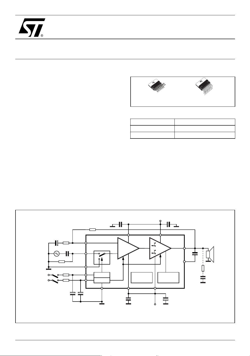
Figure 2. Typical Application and Test Circuit
gure 1. Package
Multiwatt15V
Multiwatt15H
(Short Leads)
Table 1. Order Codes
Part Number Package
TDA7296 Multiwatt15V
TDA7296HS Multiwatt15H (Short Leads)
Thanks to the wide voltage range and to the high
out current capability it is able to supply the highest power into both 4Ω and 8Ω loads even in presence of poor supply regulation, with high Supply
Voltage Rejection.
The built in muting function with turn on delay simplifies the remote operation avoiding switching onoff noises.
VM
VSTBY
February 2005
+VsC7 100nF C6 1000µF
R3 22K
C2
R2
22µF
680Ω
C1 470nF
R1 22K
R5 10K
R4 22K
C3 10µF C4 10µF
Note: The Boucherot cell R6, C10, normally not necessary for a stable operation it could
be needed in presence of particular load impedances at V
IN- 2
IN+
IN+MUTE
MUTE
STBY
3
4
10
MUTE
9
STBY
1
STBY-GND
713
-
+
THERMAL
SHUTDOWN
-Vs -PWVs
C9 100nF C8 1000µF
<±25V.
S
+PWVs+Vs
PROTECTION
158
-Vs
S/C
14
OUT
C5
22µF
6
BOOTSTRAP
D93AU011
R6
2.7Ω
C10
100nF
Rev. 10
1/15
Page 2
TDA7296
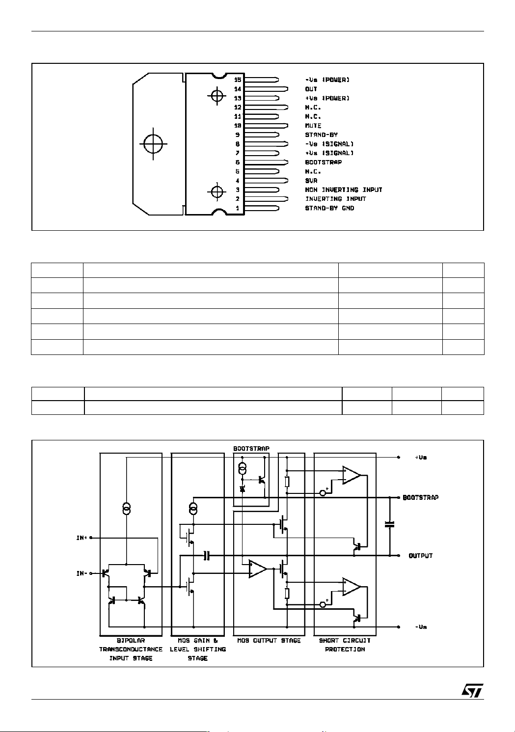
Figure 3. Pin Connection
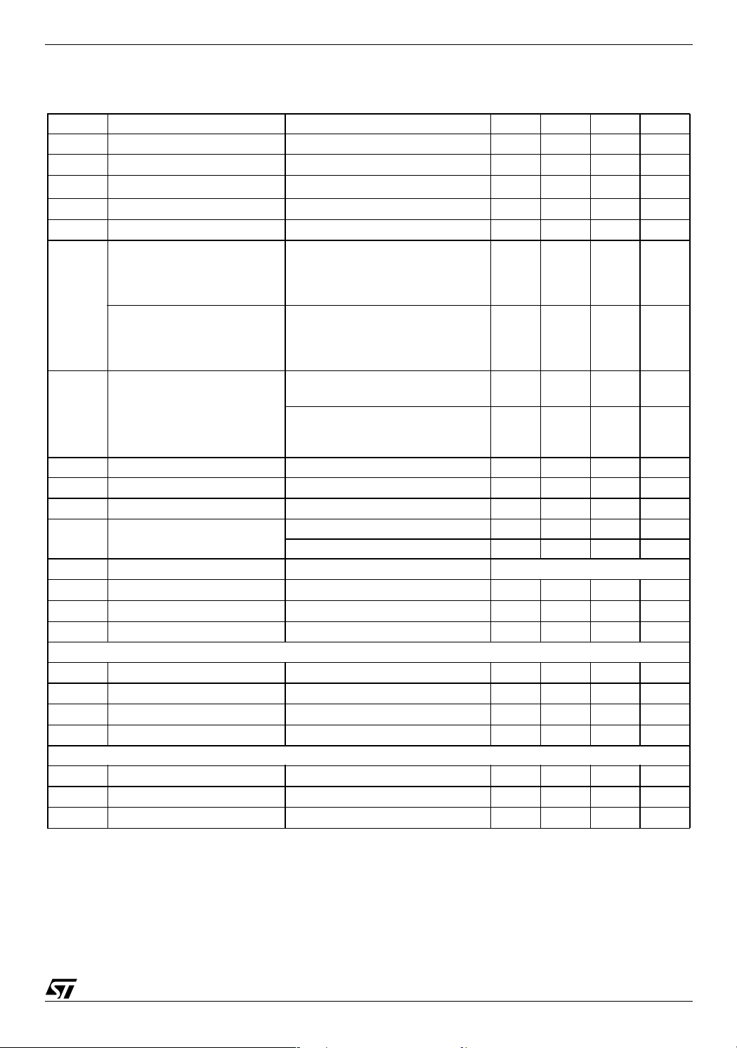
Table 2. Absolute Maximum Ratings
Symbol Parameter Value Unit
V
I
O
P
tot
T
op
T
stg
Supply Voltage (No Signal) ±35 V
S
Output Peak Current 5 A
Power Dissipation T
= 70°C 50 W
case
Operating Ambient Temperature Range 0 to 70 °C
, TjStorage and Junction Temperature 150 °C
Table 3. Thermal Data
Symbol Parameter Typ. Max Unit
R
th j-case
Thermal Resistance Junction-case 1 1.5 °C/W
Figure 4. Block Diagram
2/15
Page 3
TDA7296
Table 4. Electrical Characteristcs (Refer to the Test Circuit VS = ±24V, RL = 8Ω, GV = 30dB; Rg = 50Ω;
= 25°C, f = 1 kHz; unless otherwise specified).
T
amb
Symbol Parameter Test Condition Min. Typ. Max. Unit
V
V
I
P
SR Slew Rate 7 10 V/µs
G
G
f
L ,fH
SVR Supply Voltage Rejection f = 100Hz; V
STAND-BY FUNCTION (Ref: -Vs or GND)
V
ST on
V
ST off
AT T
I
q st-by
MUTE FUNCTION (Ref: -Vs ro GND)
V
V
AT T
Note (*):
MUSIC POWER is the maximal power which the amplifier is capable of producing across the rated load resistance (regardless of non linearity)
1 sec after the application of a sinusoidal input signal of frequency 1KHz.
Supply Range ±10 ±35 V
S
I
Quiescent Current 20 30 65 mA
q
I
Input Bias Current 500 nA
b
Input Offset Voltage -10 10 mV
OS
Input Offset Current -100 100 nA
OS
RMS Continuous Output
O
Power
Music Power (RMS)
∆t = 1s (*)
d Total Harmonic Distortion (**) P
d = 05%
= ± 24V, RL = 8Ω;
V
S
V
= ± 21V, RL = 6Ω;
S
VS = ± 18V, RL = 4Ω;
d = 10%
= ± 29V, RL = 8Ω;
V
S
V
= ± 24V, RL = 6Ω;
S
V
= ± 22V, RL = 4Ω;
S
= 5W; f = 1kHz
O
27
27
27
30
30
30
60
60
60
0.005
PO = 0.1 to 20W; f = 20Hz to 20kHz
V
= ± 18V, RL = 4Ω;
S
PO = 5W; f = 1kHz
P
= 0.1 to 20W; f = 20Hz to 20kHz
O
Open Loop Voltage Gain 80 dB
V
Closed Loop Voltage Gain (1) 24 30 40 dB
V
e
Total Input Noise A = curve 1 µV
N
0.01
f = 20Hz to 20kHz 2 5 µV
frequency response (-3dB) PO =1W 20Hz to 20kHz
R
Input Resistance 100 kΩ
i
= 0.5Vrms 60 75 dB
ripple
T
Thermal Shutdown 145 °C
S
Stand-by on Threshold 1.5 V
Stand-by off Threshold 3.5 V
Stand-by Attenuation 70 90 dB
st-by
Quiescent Current @ Stand-by 1 3 mA
Mute on Threshold 1.5 V
Mon
Mute off Threshold 3.5 V
Moff
Mute AttenuatIon 60 80 dB
mute
0.1
0.1
W
W
W
W
W
W
%
%
%
Note (**): Tested with optimized Application Board (see fig.5)
3/15
Page 4
TDA7296
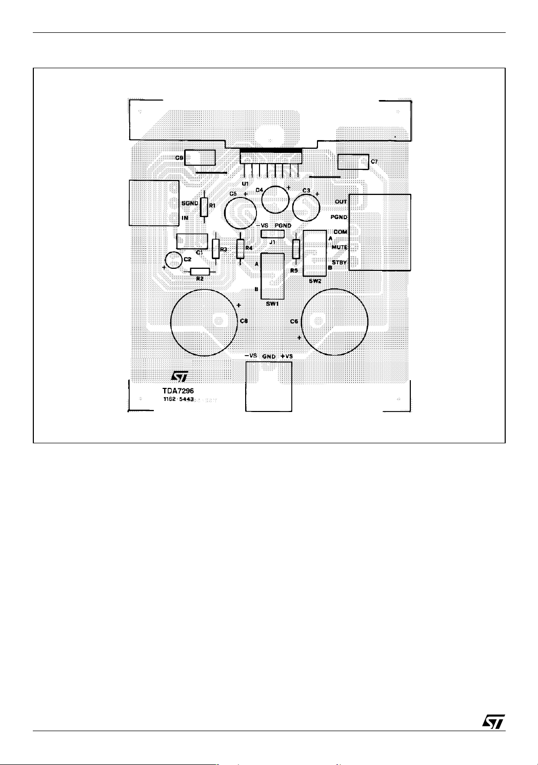
Figure 5. P.C.B. and Components Layout of the Circuit of figure 2.
Note:
The Stand-by and Mute functions can be referred either to GND or -VS.
On the P.C.B. is possible to set both the configuration through the jumper J1.
4/15
Page 5

TDA7296
3 APPLICATION SUGGESTIONS
(see Test and Application Circuits of the Fig. 2)
The recommended values of the external components are those shown on the application circuit of Figure
2. Different values can be used; the following table can help the designer.
COMPONENTS
R1 (*) 22k Input Resistance Increase Input
R2 680Ω Closed Loop Gain
R3 (*) 22k Increase of Gain Decrease of Gain
R4 22k St-by Time Constant Larger St-by
R5 10k Mute Time Constant Larger Mute
C1 0.47µF Input DC Decoupling Higher Low Frequency
C2 22µF Feedback DC
C3 10µF Mute Time Constant Larger Mute
C4 10µF St-by Time Constant Larger St-by
C5 22µF Bootstrapping Signal Degradation at
SUGGESTED
VALUE
PURPOSE
Set to 30db (**)
Decoupling
LARGER THAN
SUGGESTED
Impedance
Decrease of Gain Increase of Gain
ON/OFF Time
ON/OFF Time
ON/OFF Time
ON/OFF Time
SMALLER THAN
SUGGESTED
Decrease Input
Impedance
Smaller St-by ON/OFF
Time; Pop Noise
Smaller Mute
ON/OFF Time
Higher Low Frequency
Smaller Mute ON/OFF
Smaller St-by ON/OFF
Time; Pop Noise
Low Frequency
Cutoff
Cutoff
Time
C6, C8 1000µF Supply Voltage Bypass Danger of Oscillation
C7, C9 0.1µF Supply Voltage Bypass Danger of Oscillation
(*) R1 = R3 for pop optimization
(**) Closed Loop Gain has to be ≥ 24dB
5/15
Page 6
TDA7296
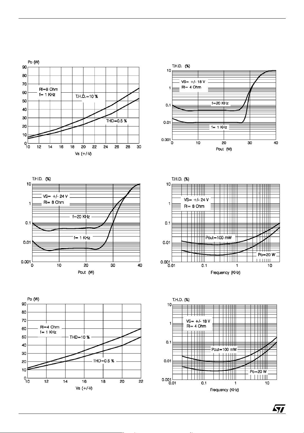
4 TYPICAL CHARACTERISTICS
(Application Circuit of fig 2 unless otherwise specified)
Figure 6. : Output Power vs. Supply Voltage.
Figure 9. Distortion vs. Output Power
Figure 7. Distortion vs. Output Power
Figure 8. Output Power vs. Supply Voltage
Figure 10. Distortion vs. Frequency
Figure 11. Distortion vs. Frequency
6/15
Page 7
TDA7296
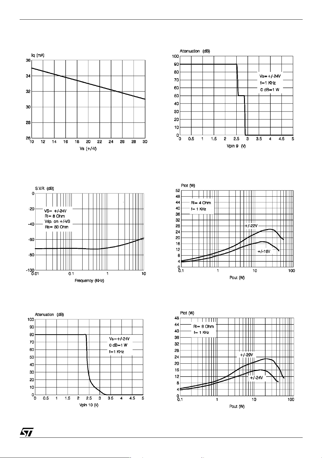
Figure 12. Quiescent Current vs. Supply
Voltage
Figure 13. Supply Voltage Rejection vs.
Frequency
Figure 15. St-by Attenuation vs. V
pin9
Figure 16. Power Dissipation vs. Output Power
Figure 14. Mute Attenuation vs. V
pin10
Figure 17. Power Dissipation vs. Output Power
7/15
Page 8

TDA7296
5 INTRODUCTION
In consumer electronics, an increasing demand has arisen for very high power monolithic audio amplifiers
able to match, with a low cost the performance obtained from the best discrete designs.
The task of realizing this linear integrated circuit in conventional bipolar technology is made extremely difficult by the occurence of 2nd breakdown phenomenon. It limits the safe operating area (SOA) of the power devices, and as a consequence, the maximum attainable output power, especially in presence of highly
reactive loads. Moreover, full exploitation of the SOA translates into a substantial increase in circuit and
layout complexity due to the need for sophisticated protection circuits.
To overcome these substantial drawbacks, the use of power MOS devices, which are immune from secondary breakdown is highly desirable. The device described has therefore been developed in a mixed bipolar-MOS high voltage technology called BCD 80.
5.1 Output Stage
The main design task one is confronted with while developing an integrated circuit as a power operational
amplifier, independently of the technology used, is that of realising the output stage. The solution shown
as a principle schematic by Fig 18 represents the DMOS unity-gain output buffer of the TDA7296.
This large-signal, high-power buffer must be capable of handling extremely high current and voltage levels
while maintaining acceptably low harmonic distortion and good behaviour over frequency response; moreover, an accurate control of quiescent current is required.
A local linearizing feedback, provided by differential amplifier A, is used to fullfil the above requirements,
allowing a simple and effective quiescent current setting. Proper biasing of the power output transistors
alone is however not enough to guarantee the absence of crossover distortion. While a linearization of the
DC transfer characteristic of the stage is obtained, the dynamic behaviour of the system must be taken
into account.
A significant aid in keeping the distortion contributed by the final stage as low as possible is provided by
the compensation scheme, which exploits the direct connection of the Miller capacitor at the amplifier’s
output to introduce a local AC feedback path enclosing the output stage itself.
5.2 Protections
In designing a power IC, particular attention must be reserved to the circuits devoted to protection of the
device from short circuit or overload conditions.
Due to the absence of the 2nd breakdown phenomenon, the SOA of the power DMOS transistors is delimited only by a maximum dissipation curve dependent on the duration of the applied stimulus.
In order to fully exploit the capabilities of the power transistors, the protection scheme implemented in this
device combines a conventional SOA protection circuit with a novel local temperature sensing technique
which " dynamically" controls the maximum dissipation.
Figure 18. Principle Schematic of a DMOS Unity-gain Buffer.
8/15
Page 9

Figure 19. Turn ON/OFF Suggested Sequence
+Vs
(V)
+35
-35
-Vs
V
IN
(mV)
V
ST-BY
PIN #9
(V)
5V
TDA7296
V
MUTE
PIN #10
(V)
I
P
(mA)
V
OUT
(V)
5V
OFF
ST-BY
PLAY
MUTE MUTE
ST-BY OFF
D93AU013
In addition to the overload protection described above, the device features a thermal shutdown circuit
which initially puts the device into a muting state (@ Tj = 145°C) and then into stand-by (@ Tj = 150°C).
Full protection against electrostatic discharges on every pin is included.
5.3 Other Features
The device is provided with both stand-by and mute functions, independently driven by two CMOS logic
compatible input pins.
The circuits dedicated to the switching on and off of the amplifier have been carefully optimized to avoid
any kind of uncontrolled audible transient at the output.
The sequence that we recommend during the ON/OFF transients is shown by Figure 19.
The application of figure 20 shows the possibility of using only one command for both st-by and mute functions. On both the pins, the maximum applicable range corresponds to the operating supply voltage.
9/15
Page 10

TDA7296
Figure 20. Single Signal ST-BY/MUTE Control Circuit
MUTE/
20K
ST-BY
10K 30K
MUTE STBY
1N4148
10µF10µF
D93AU014
6 BRIDGE APPLICATION
Another application suggestion is the BRIDGE configuration, where two TDA7296 are used, as shown by
the schematic diagram.
In this application, the value of the load must not be lower than 8 Ohm for dissipation and current capability
reasons. A suitable field of application includes HI-FI/TV subwoofers realizations. The main advantages
offered by this solution are:
– High power performances with limited supply voltage level.
– Considerably high output power even with high load values (i.e. 16 Ohm).
The characteristics shown by figures 23 and 24, measured with loads respectively 8 Ohm and 16 Ohm.
With R
±24V the maximum Pout is 60W.
Figure 21. Bridge Application Circuit
= 8 Ohm, Vs = ±18V the maximum output power obtainable is 60W, while with Rl=16 Ohm, Vs =
l
+Vs
Vi
ST-BY/MUTE
10K 30K
20K
22µF
1N4148
0.56µF 22K
2200µF0.22µF
3
22K0.56µF
1
4
10
9
9
10
22µF
3
1
4
137
+
-
15 8
+
-
137
815
6
14
2
2200µF
6
14
2
22µF
22K
680
22K
-Vs
0.22µF
22µF
22K
680
D93AU015A
10/15
Page 11

TDA7296
Figure 22. Frequency Response of the Bridge
Application
Figure 23. Distortion vs. Output Power
Figure 24. Distortion vs. Output Power
11/15
Page 12

TDA7296
Figure 25. Multiwatt15V Mechanical Data & Package Dimensions
DIM.
A5 0.197
B 2.65 0.104
C 1.6 0.063
D 1 0.039
E 0.49 0.55 0.019 0.022
F 0.66 0.75 0.026 0.030
G 1.02 1.27 1.52 0.040 0.050 0.060
G1 17.53 17.78 18.03 0.690 0.700 0.710
H1 19.6 0.772
H2 20.2 0.795
L 21.9 22.2 22.5 0.862 0.874 0.886
L1 21.7 22.1 22.5 0.854 0.87 0.886
L2 17.65 18.1 0.695 0.713
L3 17.25 17.5 17.75 0.679 0.689 0.699
L4 10.3 10.7 10.9 0.406 0.421 0.429
L7 2.65 2.9 0.104 0.114
M 4.25 4.55 4.85 0.167 0.179 0.191
M1 4.73 5.08 5.43 0.186 0.200 0.214
S 1.9 2.6 0.075 0.102
S1 1.9 2.6 0.075 0.102
Dia1 3.65 3.85 0.144 0.152
mm inch
MIN. TYP. MAX. MIN. TYP. MAX.
OUTLINE AND
MECHANICAL DATA
Multiwatt15 (Vertical)
12/15
0016036 J
Page 13

Figure 26. Multiwatt15 Horizontal (Short leads) Mechanical Data & Package Dimensions
TDA7296
DIM.
mm inch
MIN. TYP. MAX. MIN. TYP. MAX.
A50.197
B 2.65 0.104
C1.60.063
E 0.49 0.55 0.019 0.022
F 0.66 0.75 0.026 0.030
G 1.02 1.27 1.52 0.040 0.050 0.060
G1 17.53 17.78 18.03 0.690 0.700 0.709
H1 19.6 20.2 0.772 0.795
H2 19.6 20.2 0.772 0.795
L1 17.80 18.00 18.20 0.701 0.709 0.717
L2 2.54 0.100
L3 17.25 17.5 17.75 0.679 0.689 0.699
L4 10.3 10.7 10.9 0.406 0.421 0.429
L5 2.70 3.00 3.30 0.106 0.118 0.130
L7 2.65 2.9 0.104 0.114
R 1.5 0.059
S 1.9 2.6 0.075 0.102
S1 1.9 2.6 0.075 0.102
Multiwatt15 H (Short leads)
Dia1 3.65 3.85 0.144 0.152
OUTLINE AND
MECHANICAL DATA
H2
V
R
R
B
L5
F
G1
G
V
E
N
V V
C
L1L2
L3
L4
R1 P
L7
Diam 1
S1
V
A
H2
H1
S
MW15HME
0067558 E
13/15
Page 14

TDA7296
Table 5. Revision History
Date Revision Description of Changes
January 2004 8 First Issue in EDOCS DMS
September 2004 9 Added Package Multiwatt15 Horizontal (Short leads)
February 2005 10 Corrected mistyping error in Table 2.
14/15
Page 15

TDA7296
Information furnished is believed to be accurate and reliable. However, STMicroelectronics assumes no responsibility for the consequences
of use of such information nor for any infringement of patents or other rights of third parties which may result from its use. No license is granted
by implication or otherwise under any patent or patent rights of STMicroelectronics. Specifications mentioned in this publication are subject
to change without notice. This publication supersedes and replaces all information previously supplied. STMicroelectronics products are not
authorized for use as critical components in life support devices or systems without express written approval of STMicroelectronics.
The ST logo is a registered trademark of STMicroelectronics.
All other names are the property of their respective owners
© 2005 STMicroelectronics - All rights reserved
Australia - Belgium - Brazil - Canada - China - Czech Republic - Finland - France - Germany - Hong Kong - India - Israel - Italy - Japan -
Malaysia - Malta - Morocco - Singapore - Spain - Sweden - Switzerland - United Kingdom - United States of America
STMicroelectronics group of companies
www.st.com
15/15
 Loading...