

Page 1

1 FEATURES
V
F
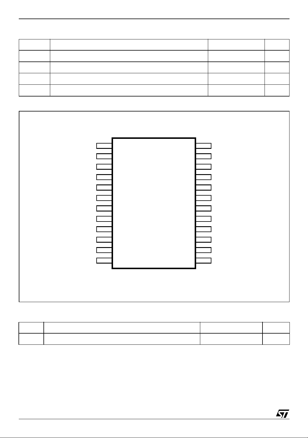
Figure 1. Package
T
■ TECHNOLOGY BI20II
■ WIDE SUPPLY VOLTAGE RA NGE (3 .5 - 12V)
■ OUTPUT POWER:
– 3+3W @THD = 10%, R
– 4+4W Music Power @THD = 10%, R
V
= 8.5V
CC
■ SINGLE SUPPLY
■ MINIMUM EXTERNAL COMPONENTS:
= 8Ω, VCC = 7.5V
L
= 8Ω,
L
– NO SVR CAPACITOR
– NO BOOTSTRA P
– NO BOUCHEROT CELLS
– INTERNALLY FIXED GAIN
■ STAND-BY & MUTE FUNCTIONS
■ SHORT CIRCUIT PROTECTION
■ THERMAL OVERLOAD PR OTEC TION
TDA7266P
3+3W DUAL BRIDGE AMPLIFIER
PRODUCT PREVIEW
PowerSSO24 (Slug Down)
able 1. Order Codes
Part Number Package
TDA7266P PowerSSO24 (Slug Down)
2 DESCRIPTION
The TDA7266P is a dual bridge amplifier specially
designed for LCD TV/Monitor, PC Motherboard, TV
and Portable Audio applications.
Figure 2. Tes t an d A pp li cat io n D i agram
CC
+5V
ST-BY
MUTE
IN2
C3 0.22µF
R3 10K
C4
10µF
C5 0.22µF
R4 10K
C6
1µF
PW-GND
S-GND
8
14
11
17
10
1
24
Vref
187
+
-
-
+
+
-
-
+
5
6
20
19
C1
470µFC2100nF
OUT1+
OUT1-
OUT2+
OUT2-
D03AU1531A
C7
100n
July 2004
This is preliminary information on a new product foreseen to be developed. Details are subject to change without notice.
REV. 2
1/12
Page 2
TDA7266P
D
P
Table 2. Absolute Maximum Ratings
Symbol Parameter Value Unit
Supply Voltage 20 V
s
Output Peak Current (internally limited) 1.5 A
Operating Temperature 0 to 70 °C
Storage and Junction Temperature -40 to 150 °C
T
T
stg, Tj
V
I
O
op
Figure 3. Pin Connection (Top view)
W GND
N.C.
N.C.
N.C.
OUT1+
OUT1-
+V
S
IN1
1
2
3
4
5
6
7
8
24
23
22
21
20
19
18
17
PW GN
N.C.
N.C.
N.C.
OUT2+
OUT2+V
S
IN2
9
16
15MUTE
STBY
N.C.
11
12
14
13
D03AU1532
N.C.N.C.
N.C.10
SGND
N.C.
Table 3. Themal Data
Symbol Parameters Value Unit
R
th j-case
Thermal Resistance Junction to Case Typ. 1.5 °C/W
2/12
Page 3

TDA7266P
Table 4.
(Refer to te st circuit; VCC = 7.5V, RL = 8Ω, f = 1KHz, T
Electrical Characteristcs
= 25°C unless otherwise specified)
amb
Symbol Parameter Test Condition Min. Typ. Max. Unit
V
V
P
P
Supply Range 3.5 12 V
CC
Total Quiescent Current 40 mA
I
q
Output Offset Voltage 120 mV
OS
Output Power THD 10% 3 W
O
Output Music Power (*) 4 W
O
THD Total Harmonic Distortion PO = 1W 0.03 0.2 %
PO = 0.1W to 2W
1%
f = 100Hz to 15KHz
SVR Supply Voltage Rejection f = 100Hz, VR =0.5V 40 56 dB
CT Crosstalk 46 60 dB
A
MUTE
G
Mute Attenuation 60 80 dB
T
Thermal Threshold 150 °C
w
Closed Loop Voltage Gain 25 26 27 dB
V
∆G
VT
VT
I
ST-BY
(*) Measured on demoboard of figure 8 wi th gaussian noi se signal whi ch simulates M usic/Speec h programmes.
Voltage Gain Matching 0.5 dB
V
R
Input Resistance 25 30 K Ω
i
Mute Threshold for VCC > 6.4V; Vo = -30dB 2.3 2.9 4.1 V
MUTE
< 6.4V; Vo = -30dB VCC/2-1VCC/2
for V
CC
St-by Threshold 0.8 1.3 1.8 V
ST-BY
St-by Current V6 = GND 100 µA
e
Total Output Voltage A Curve 150 µV
N
-0.75
VCC/2
-0.5
V
3/12
Page 4

TDA7266P
F
3 APPLICATIVE SUG GESTIONS
3.1 STAND-BY AND MUTE FUNCTIONS
3.1.1 (A) Microprocessor Application
In order to avoid annoying "Pop-Noise" during Turn-On/Off transients, it is necessary to guarantee the right Stby and mute signals seque nce.It is quite simpl e to obtain this function using a microprocessor (Fig. 4 and 5).
At first St-by signal (f rom
exponentially. The external RC network is intended to turn-on slowly the biasing circuits of the amplifier, this to
avoid "POP" and "CLICK" on the outputs.
When this voltage reaches the St-by threshold level, the amplifier is switched-on and the external capacitors in
series to the input terminals (C1, C3) start to charge.
It's necessary to mantain the mute signal low until the capacitors are fully charged, this to avoid that the device
goes in play mode causing a loud "Pop Noise" on the speakers.
A delay of 100-200ms between St-by and mute signals is suitable for a proper operation.
Figure 4. Microprocessor Application
µ
P) goes high and the voltage across the St-by terminal (Pin 11) starts to increase
V
CC
µP
ST-BY
MUTE
IN1
R1 10K
IN2
R2 10K
PW-GND
C1 0.22µF
C2
10µF
C3 0.22µF
C4
1µF
S-GND
8
11
14
17
10
1
24
Vref
187
+
-
-
+
+
-
-
+
5
6
20
19
C5
470µFC6100n
OUT1+
OUT1-
OUT2+
OUT2-
D03AU1533
4/12
Page 5

Figure 5. Microprocessor Driving S ignals
+
A
VS(V)
+7.5
V
IN
(mV)
V
ST-BY
pin 11
1.8
1.3
0.8
V
MUTE
pin 10
4.1
2.9
2.3
TDA7266P
I
q
(mA)
V
OUT
(V)
OFF
ST-BY
PLAY MUTE ST-BY
MUTE
OFF
D03AU1535
3.1.2 B) Low Cost Application
In low cost applications where the µP is not present, the suggested circuit is shown in fig.6.
The St-by and mute terminals are tied together and they are connected to the supply line via an external voltage
divider.
The device is switched-on/off from the supply line and the external capacitor C4 is intended to delay the St-by
and mute threshold exceeding, avoiding "Popping" problems.
So to avoid any popping or clicking sond, it is important to clock:
a Correct Sequenc e: At turn-ON, the Stand-by must be removed a t first, then the M ute must be re-
leased after a delay of abo ut 100-200ms . On the contrary at t urn-OFF the M ute must be a ctivated
as first and then the Stand-by.
With the values suggested in the Application circuit the right operation is guaranteed.
b Correct Threshold Voltages: In order to avoid that due to the spread in the internal thresholds (see
the above li mits) a wrong external voltage caus es uncertain commu tations f or the two functions we
suggest to use the following values:
Mute for Vc c>6.4V : VT = 2.3V
Mute for Vcc<6.4V : V T = Vcc/2 - 1
Stand-by : VT = 0.8V
5/12
Page 6

TDA7266P
F
V
F
Figure 6. Sta nd-alone low-cost Applica tio n
V
CC
R1
24K
R2
47K
C4
10µF
C3 0.22µF
IN1
C5 0.22µF
IN2
PW-GND
ST-BY
S-GND
MUTE
8
11
14
Vref
17
10
1
24
+
-
-
+
+
-
-
+
187
5
6
20
19
C1
470µFC2100nF
OUT1+
OUT1-
OUT2+
OUT2-
D03AU1534A
C7
100n
Figure 7. Applicat i on Circ uit
CC
R1
+5V
JP1
R2
ST-BY
MUTE
IN1
IN2
C3 0.22µF
R3 10K
C4
10µF
C5 0.22µF
R4 10K
C6
1µF
PW-GND
S-GND
8
14
11
Vref
17
10
1
24
+
-
+
+
-
+
187
5
6
20
19
C1
470µFC2100nF
OUT1+
OUT1-
OUT2+
OUT2-
D03AU1551
C7
100n
6/12
Page 7

Figure 8. PCB Component Layout
Figure 9. PCB Copper Top (Top view)
TDA7266P
Figure 10. PCB Copper Bottom (Top view)
7/12
Page 8

TDA7266P
P
2
4 PCB LAYOUT AND EXTERNAL COMPONENTS
Regarding the PCB layout care must be taken for three main subjects:
1) Signal and Power Gnd separation
2) Dissipating Copper Area
3) Filter Capacitors positioning
1) Signal and Power Gnd separation:
To the Signal GND must be referred the Audio Input Signals, the Mute and Stand-b y Voltages and t he
device PIN.14. This Gnd path must be as clean as possible in order to improve the device THD+Noise
and to avoid spurious oscillations across the speakers.
The Power GND is di rectly con nected to th e Ou tput power Stage transistors (Emitters) and is cros sed
by large amount of current , thi s pat h is al so used in this device to dissipate the heating generat ed (no
needs of external heatsinker).
Referring to the typical application circuit, the separation between the two GND paths must be obtained
connecting them separately (star routing) to the bulk
Electrolithic capacitor C1 (470µF).
Regarding the Power Gnd dimensioning we have to consider the Dissipated Power the Thermal Protection Threshold and the Package thermal Characteristics.
2) Dissipating Copper Area:
Dissipated Power:
The max dissipated power happens for a THD near 1% and is given by the formula:
V
CC
------------- - I
dmax W()
2
π
2Rl
----- -
+⋅=
qVCC
2
This gives fo r: V cc = 7.5V, Rl = 8Ω ,Iq = 40mA a dissipated power of Pd = 3W.
Thermal Protection:
The thermal protection threshold is placed at a junction temperature of 150°C.
Package Thermal Characteristics:
The thermal resistance Junction to Ambient obtainable with a GND copper Area of 3x3 cm and with 16 via
holes (see picture) is about 25° C/W. This means that with the above menti oned max dissipated Power
(Pd=3W) we can expect a 75°C, this gives a safety margin before the thermal protection intervention in the
consumer environments where a 50°C ambient is specified as maximum
Figure 11.
3)Filter Capacitors Positioning:
The two Ceramic capacitors C2/C7 (100nF) must be placed as close as possible
respectively to the t wo V cc pins ( 7 - 18) in orde r to avoi d the pos sibiltiy of osc illations arising on the
output Audio signals.
8/12
Page 9

TDA7266P
20k
T
100k
L
5
4
-
-
-
Attenuation (dB)
5 TYPICAL CHARACTERISTICS
(Referred to application circuit of figure 8 unless otherwise specified)
Figure 12. Distortion vs Frequency
HD(%)
10
Vcc = 7.5V
1
0.1
0.010
Rl = 8 ohm
Pout = 100mW
Pout = 2W
100 1k 10k
frequency (Hz)
Figure 13. Distortion vs Output Power
10
%
5
Vs= 7.5V
Rl= 8 Ohm
2
F= 1 KHz
1
0.5
0.2
0.1
0.05
0.02
0.01
100m 3200m 300m 400m500m 700m 1 2
W
Figure 15. Gain vs Frequency
evel(dBr)
5.0000
4.0000
3.0000
2.0000
1.0000
0.0
-1.000
-2.000
-3.000
-4.000
-5.000
10 100 1k 10k
Vcc = 7.5V
Rl = 8 ohm
Pout = 1W
frequency (Hz)
Figu r e 1 6 . Mute Attenu a tion vs Vpin.10
Attenuation (dB)
10
0
-10
-20
-30
-40
-50
-60
-70
-80
-90
00
11.522.533.544.5
Vpin.10(V)
Figure 14. Distortion vs Output Power
%
%
10
10
5
5
Vs= 8 .5V
Vs= 8 .5V
2
2
Rl= 8 Ohm
Rl= 8 Ohm
F= 1 KHz
F= 1 KHz
1
1
0.5
0.5
0.2
0.2
0.1
0.1
0.05
0.05
0.02
0.02
0.01
0.01
100m 4200m 300m 400m 600m 800m 1 2 3
100m 4200m 300m 400m 600m 800m 1 2 3
W
W
Figure 17. Stand-By attenuation vs Vpin 11
10
0
-10
-20
-30
-40
-50
-60
-70
-80
-90
100
110
120
0 0.2 0.4 0.6 0.8 1 1.2 1.4 1.6 1.8 2 2.2 2.
Vpin.11 (V)
9/12
Page 10

TDA7266P
Figure 18. PowerSSO24 Mechanic al Data & Package Dimension s
DIM.
A 2.15 2.47 0.084 0.097
A2 2.15 2.40 0.084 0.094
a100.07500.003
b 0.33 0.51 0.013 0.020
c 0.23 0.32 0.009 0.012
(1)
10.10 10.50 0.398 0.413
D
(1)
E
e 0.8 0.031
e3 8.8 0.346
G 0.10 0.004
G1 0.06 0.002
H 10.10 10.50 0.398 0.413
h 0.40 0.016
L 0.55 0.85 0.022 0.033
N 10˚ (max)
X 4.10 4.70 0.161 0.185
Y 6.50 7.10 0.256 0.279
(1) “D and E1 ” do not include mol d flash or protusions.
Mold flash or p rot usions shall not exceed 0.15m m (0.006”)
(2) No intrusion allowed inwards the leads.
(3) Flash or bleeds on exposed die pad shall not exceed 0.4 mm
per side
mm inch
MIN. TYP. MAX. MIN. TYP. MAX.
7.4 7.6 0.291 0.299
OUTLINE AND
MECHANICAL DATA
PowerSSO24
10/12
7412828 A
Page 11

Table 5. Revision History
Date Revision Description of Changes
May 2004 1 First Issue
July 2004 2 Electrical Characteristics: Deleted TYP. Value VCC
TDA7266P
11/12
Page 12

TDA7266P
Information furnished is believed to be accurate and reliable. However, STMicroelectronics assumes no responsibility for the consequences
of use of such information nor for any infringement of patents or other rights of third parties which may result from its use. No license is granted
by implic ation or oth erwise under any patent or pate nt rights of STMicroe l ectronics. Specificat i ons mentioned in thi s publication are subject
to change without notice. This publication supersedes and replaces all information previously supplied. STMicroelectronics products are not
authorized for use as critical comp onents in life support devi ces or systems wi t h out express wri t ten approva l of STMicroelectronics.
The ST logo is a register ed trademark of S T M i croelectroni cs.
All other nam es are the pro perty of their respectiv e owners
© 2004 STMi croelectro ni cs - All rights res erved
Australi a - Belgium - B razil - Canad a - China - Czech Republic - F i nl and - France - Germany - Hong Kong - India - Israel - Ital y - Japan -
Malaysia - Malta - Morocco - Singapore - Spain - Sweden - Switzerland - United Kingdom - United States
STMicroelectronics GROUP OF COMPANIES
www.st.com
12/12
 Loading...