

TDA7233
Fi
1W AUDIO AMPLIFIER WITH MUTE
1 FEATURES
OPERATING VOLTAGE 1.8 TO 15 V
EXTERNAL MUTE OR POWER DOWN
FUNCTION
IMPROVED SUPPLY VOLTAGE REJECTION
LOW QUIESCENT CURRENT
HIGH POWER CAPABILITY
LOW CROSSOVER DISTORTION
2 DESCRIPTION
The TDA7233/D is a monolithic integrated circuit
in 8 pin Minidip or SO8 package, intended for use
as class AB power amplifier with a wide range of
supply voltage from 1.8V to 15V in portable players, cordless telephones and Cellular Radios.
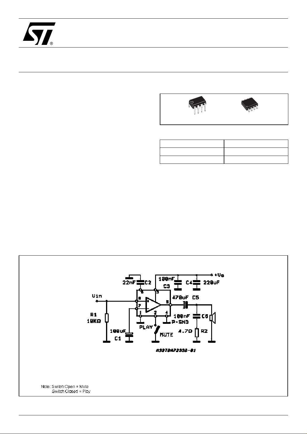
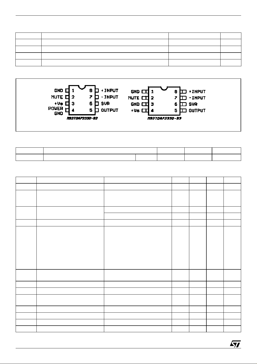
Figure 2. Pin Connection
gure 1. Package
Minidip
Table 1. Order Codes
Part Number Package
TDA7233 Minidip
TDA7233D SO8
SO8
May 2010
REV. 4
1/8
TDA7233
Table 2. Absolute Maximum Ratings
Symbol Parameter Value Unit
V
P
tot
I
O
T
stg
Figure 3. PIN CONNECTIONS (top view)
Supply Voltage 16 V
S
Total Power Dissipation at T
= 50 °C 1 W
amb
Output Peak Current 1 A
, TjStorage and Junction Temperature -40 to 150 °C
Minidip
SO8
Table 3. Thermal Data
Symbol Parameter SO8 MInidip Unit
R
th j-amb
Table 4. Electrical Characteristcs (V
Symbol Parameter Test Condition Min. Typ. Max. Unit
V
S
V
O
I
d
I
b
P
O
d Distortion Po = 0.5W; f = 1KHz; R
Gv Closed Loop Voltage Gain f = 1KHz; 39 dB
R
in
e
N
SVR Supply Voltage Rejection f = 100Hz; R
I
M
Thermal Resistance Junction-ambient Max. 200 100 °C/W
= 6 V, T
s
= 25 °C, unless otherwise specified)
amb
Supply Voltage 1.8 15 V
Quiescent Output Voltage
Vs = 3 V
Vs = 9 V
2.7
1.2
4.2
Quiescent Drain Current MUTE HIGH 3.6 9 mA
MUTE LOW 0.4 mA
Input Bias Current 100 nA
Output Power d = 10%; f = 1kHz
Vs = 12V; R
Vs = 9V; R
Vs = 9V; R
Vs = 6V; R
Vs = 6V; R
Vs = 3V; R
Vs = 3V; R
= 8Ω
L
= 4Ω
L
= 8Ω
L
= 8Ω
L
= 4Ω
L
= 4Ω
L
= 8Ω
L
= 8Ω
L
1.9
1.6
1
0.4
0.7
110
70
0.3 %
Vs = 9V
Input Resistance f = 1KHz; 100 KΩ
Total Input Noise Rs = 10KΩ; B = Curve A
Rs = 10KΩ; B = 22Hz to 22KHz
= 10KΩ 45 dB
g
2
3
MUTE Attenuation Vo = 1V; f = 100Hz to 10KHz; 70 dB
MUTE Threshold 0.6 V
MUTE Current Vs = 15V 0.4 mA
V
W
W
W
W
W
mW
mW
µV
µV
2/8
TDA7233
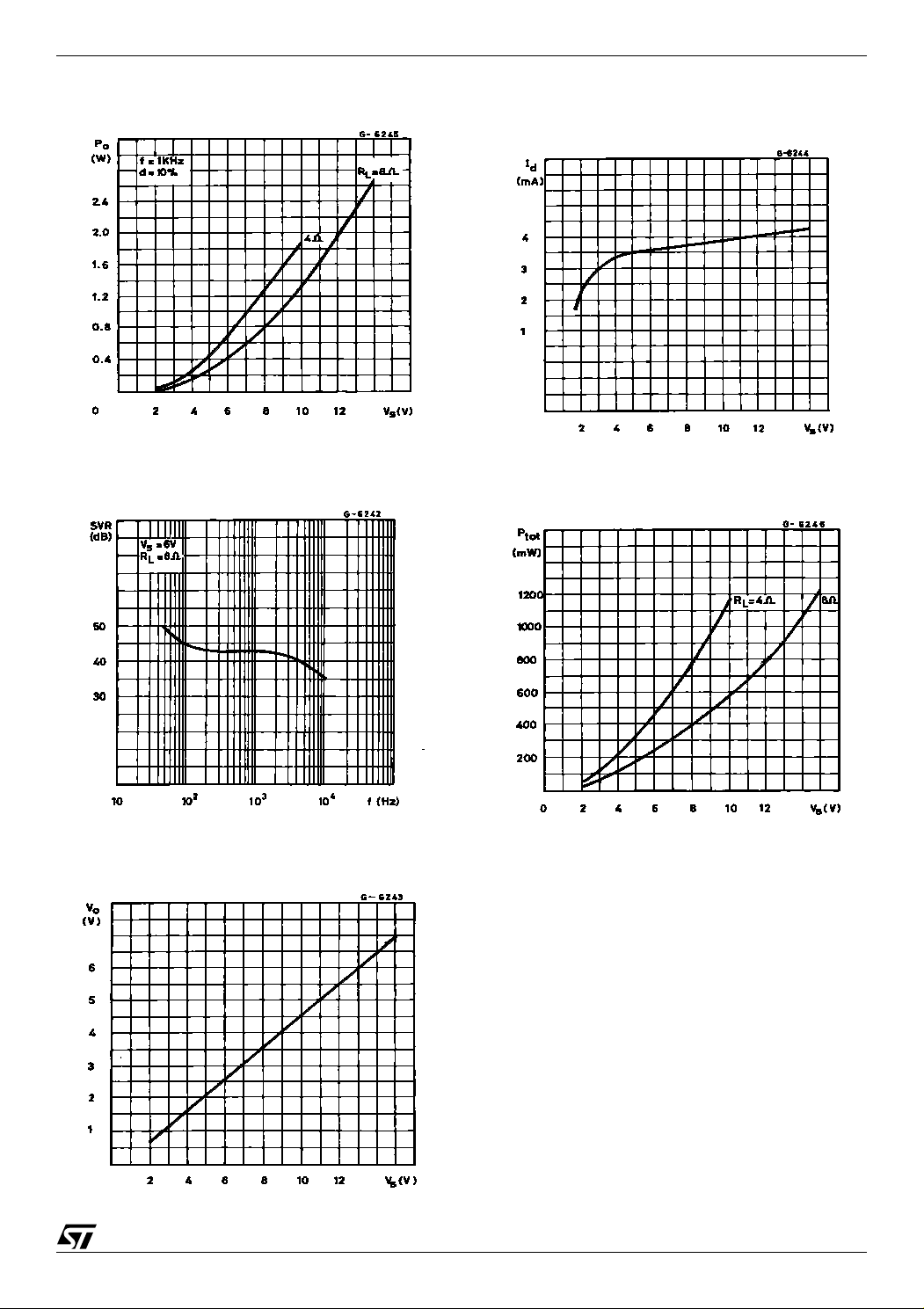
Figure 4. Output Power versus Supply Voltage
Figure 5. Supply Voltage Rejection versus
Frequency
Figure 7. Quiescent Current versus Supply
Voltage
Figure 8. Total Power Dissipated versus
Supply Voltage
Figure 6. DC Output Voltage versus Supply
Voltage
3/8

TDA7233
3 PACKAGE MECHANICAL DATA
In order to meet environmental requirements, ST offers these devices in different grades of ECOPACK
packages, depending on their level of environmental compliance. ECOPACK® specifications, grade definitions and product status are available at: www.st.com. ECOPACK
®
is an ST trademark.
®
4/8

Figure 9. Minidip Mechanical Data & Package Dimensions
TDA7233
DIM.
mm inch
MIN. TYP. MAX. MIN. TYP. MAX.
A3.32 0.131
a1 0.51 0.020
B 1.15 1.65 0.045 0.065
b 0.356 0.55 0.014 0.022
b1 0.204 0.304 0.008 0.012
D 10.92 0.430
E 7.95 9.75 0.313 0.384
e2.54 0.100
e3 7.62 0.300
e4 7.62 0.300
F 6.6 0.260
I 5.08 0.200
L 3.18 3.81 0.125 0.150
Z 1.52 0.060
OUTLINE AND
MECHANICAL DATA
Minidip
5/8

TDA7233
Figure 10. SO8 Mechanical Data & Package Dimensions
DIM.
A 1.750 0.0689
A1 0.100 0.250 0.0039 0.0098
A2 1.250 0.0492
b 0.280 0.480 0.0110 0.0189
c 0.170 0.230 0.0067 0.0091
(1)
D
E 5.800 6.000 6.200 0.2283 0.2362 0.2441
(2)
E1
e 1.270 0.0500
h 0.250 0.500 0.0098 0.0197
L 0.400 1.270 0.0157 0.0500
L1 1.040 0.0409
k0˚8˚0˚8˚
ccc 0.100 0.0039
Notes: 1. Dimensions D does not include mold flash,
protrusions or gate burrs.
Mold flash, potrusions or gate burrs shall not
exceed 0.15mm in total (both side).
2. Dimension “E1” does not include interlead flash
or protrusions. Interlead flash or protrusions shall
not exceed 0.25mm per side.
mm inch
MIN. TYP. MAX. MIN. TYP. MAX.
4.800 4.900 5.000 0.1890 0.1929 0.1969
3.800 3.900 4.000 0.1496 0.1535 0.1575
OUTLINE AND
MECHANICAL DATA
SO-8
6/8
0016023 D

4 REVISION HISTORY
Table 5. Revision History
Date Revision Description of Changes
September 2003 3 No recorded changes
TDA7233
03-May-2010 4 Updated title and added environmental compliance statement for
package
7/8

TDA7233
Please Read Carefully:
Information in this document is provided solely in connection with ST products. STMicroelectronics NV and its subsidiaries (“ST”) reserve the
right to make changes, corrections, modifications or improvements, to this document, and the products and services described herein at any
time, without notice.
All ST products are sold pursuant to ST’s terms and conditions of sale.
Purchasers are solely responsible for the choice, selection and use of the ST products and services described herein, and ST assumes no
liability whatsoever relating to the choice, selection or use of the ST products and services described herein.
No license, express or implied, by estoppel or otherwise, to any intellectual property rights is granted under this document. If any part of this
document refers to any third party products or services it shall not be deemed a license grant by ST for the use of such third party products
or services, or any intellectual property contained therein or considered as a warranty covering the use in any manner whatsoever of such
third party products or services or any intellectual property contained therein.
UNLESS OTHERWISE SET FORTH IN ST’S TERMS AND CONDITIONS OF SALE ST DISCLAIMS ANY EXPRESS OR IMPLIED
WARRANTY WITH RESPECT TO THE USE AND/OR SALE OF ST PRODUCTS INCLUDING WITHOUT LIMITATION IMPLIED
WARRANTIES OF MERCHANTABILITY, FITNESS FOR A PARTICULAR PURPOSE (AND THEIR EQUIVALENTS UNDER THE LAWS
OF ANY JURISDICTION), OR INFRINGEMENT OF ANY PATENT, COPYRIGHT OR OTHER INTELLECTUAL PROPERTY RIGHT.
UNLESS EXPRESSLY APPROVED IN WRITING BY AN AUTHORIZED ST REPRESENTATIVE, ST PRODUCTS ARE NOT
RECOMMENDED, AUTHORIZED OR WARRANTED FOR USE IN MILITARY, AIR CRAFT, SPACE, LIFE SAVING, OR LIFE
SUSTAINING APPLICATIONS, NOR IN PRODUCTS OR SYSTEMS WHERE FAILURE OR MALFUNCTION MAY RESULT IN
PERSONAL INJURY, DEATH, OR SEVERE PROPERTY OR ENVIRONMENTAL DAMAGE. ST PRODUCTS WHICH ARE NOT
SPECIFIED AS "AUTOMOTIVE GRADE" MAY ONLY BE USED IN AUTOMOTIVE APPLICATIONS AT USER’S OWN RISK.
Resale of ST products with provisions different from the statements and/or technical features set forth in this document shall immediately void
any warranty granted by ST for the ST product or service described herein and shall not create or extend in any manner whatsoever, any
liability of ST.
ST and the ST logo are trademarks or registered trademarks of ST in various countries.
Information in this document supersedes and replaces all information previously supplied.
The ST logo is a registered trademark of STMicroelectronics. All other names are the property of their respective owners.
© 2010 STMicroelectronics - All rights reserved
STMicroelectronics group of companies
Australia - Belgium - Brazil - Canada - China - Czech Republic - Finland - France - Germany - Hong Kong - India - Israel - Italy - Japan -
Malaysia - Malta - Morocco - Philippines - Singapore - Spain - Sweden - Switzerland - United Kingdom - United States of America
www.st.com
8/8
 Loading...