

现货库存、技术资料、百科信息、热点资讯,精彩尽在鼎好!
TV VERTICALDEFLECTION OUTPUT CIRCUIT
The functionsincorporatedare :
.
POWERAMPLIFIER
.
FLYBACKGENERATOR
.
REFERENCE VOLTAGE
.
THERMALPROTECTION
TDA2170
DESCRIPTION
The TDA2170 is a monolithicintegrated circuit in
11-leadMultiwatt package.It is a high efficiency
power boosterfor directdriving ofverticalwindings
of TV yokes. It is intended for use in Colour are B
& Wtelevision receivers aswell asin monitors and
displays.
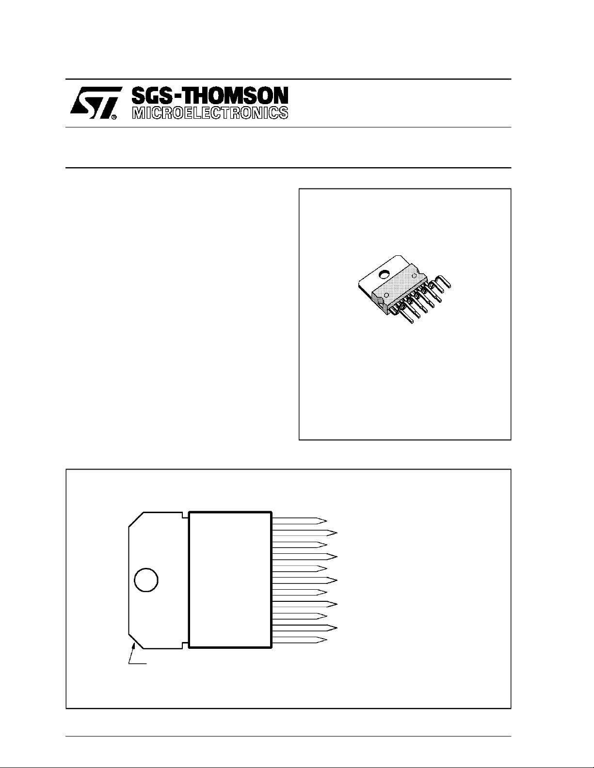
PINCONNECTIONS
11
10
9
8
7
6
5
4
3
2
1
MULTIWATT 11
(Plastic Package)
ORDER CODE : TDA2170
NC
GND
REFERENCEVOLTAGE
OUTPUTSTAGESUPPLY
OUTPUT
GND
FLYBACKGENERATOR
SUPPLYVOLTAGE
NON INVERTINGINPUT
INVERTING INPUT
NC
December 1992
Tab connected to Pin 6
2170-01.EPS
1/7
TDA2170
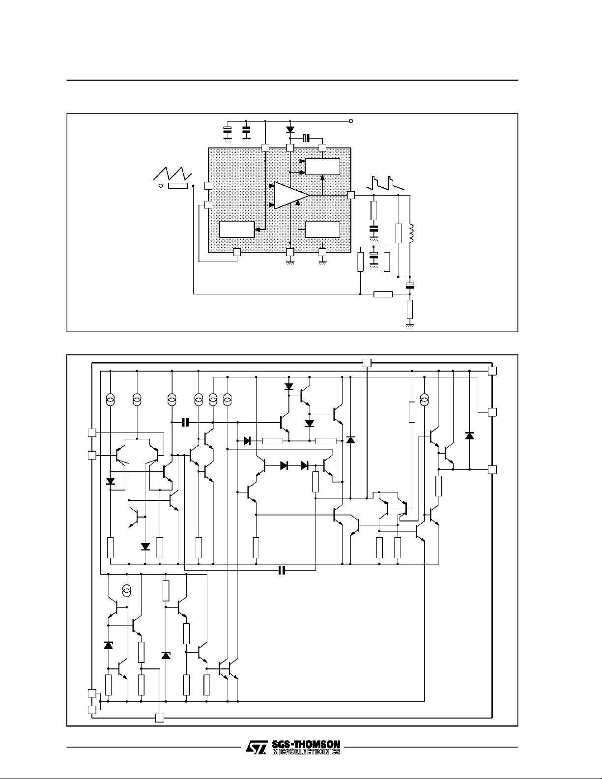
BLOCK DIAGRAM
584
Flyback
Generator
+V
S
SCHEMATIC DIAGRAM
3
2
Q1 Q2
D1
Q3
2
3
Reference
Voltage
Power
Amplifier
7
Thermal
Protection
6
109
YOKE
2170-02.EPS
7
4
D4
Q11
Q17
R12
Q20 D9
Q21
R11
Q18
Q22
Q19
R8 R9
Q12
D5
R5R4
D8
Q13
Q4
C1
Q7
D3
Q6
Q8
Q9
Q10
D6 D7
R6
Q14
Q5
Q15
Q16
R2D2R1
R3
R7
8
5
2/7
C2
R12
Q23
Q26
Q24
R14
Z1
R15
R13
Q25
R16
Q27
Q28Z2
R17 R18
Q29
6
10
9
2170-03.EPS
TDA2170
ABSOLUTEMAXIMUM RATINGS
Symbol Parameter Value Unit
V
s
V
7,V8
V
5
V2,V
I
o
I
o
I
o
I
5
I
5 Pin 5 Peak to Peak Flyback Current at f = 50 Hz, t
P
tot
T
stg,Tj
THERMALDATA
Symbol Parameter Value Unit
R
th (j-c)
R
th (j-a)
Supply Voltage (pin 4) 35 V
Flyback Peak Voltage 60 V
Voltage at Pin 5 + V
Amplifier Input Voltage + Vs– 0.5 V
3
s
Output Peak Current (non repetitive, t = 2 msec) 2.5 A
Output Peak Current at f = 50 Hz, t ≤ 10 µsec
Output Peak Current at f = 50 Hz, t > 10 µsec
Pin 5 DC Current at V7<V
Total Power Dissipation at T
4
case
=60°C
≤ 1.5 msec
fly
3A
2A
100 mA
3A
30 W
Storage and Junction Temperature – 40 to 150 °
Thermal Resistance Junction-case Max 3 °
Thermal Resistance Junction–ambient Max 40
C
C/W
°C/W
2170-01.TBL
2170-02.TBL
ELECTRICAL CHARACTERISTICS
(refer to the test circuits, V
Symbol Parameter Test Conditions Min. Typ. Max. Unit Fig.
Pin 4 Quiescent Current I5=0;I7=0;V3= 3 V 8 16 mA 1a
Pin 8 Quiescent Current I5=0;I7=0;V3=3V 16 36 mA 1a
Amplifier Input Bias Current V3= 1 V – 0.1 – 1
Amplifier Input Bias Current V2= 1 V – 0.1 – 1 µ
Reference Voltage I9= 0 2.2 V 1a
9
Reference Voltage Drift vs. Supply Voltage VS= 15 to 30 V 1 2 mV/V 1a
9
S
Pin 5 Saturation Voltage to GND I5=20mA 1 V 1c
Quiescent Output Voltage
7
Output Saturation Voltage to GND I7= 1.2 A 1 1.4 V 1c
Output Saturation Voltage to Supply – I7= 1.2 A 1.6 2.2 V 1b
Reference Voltage Output Resistance 2.1
9
Junction Temperature for Thermal Shut
j
Down
V
∆V
∆V
V
V
V
V
R
I
4
I
8
I
3
I
2
5L
7L
7H
T
=35V, T
S
=25°C unless otherwisespecified)
amb
=35V;Ra=13kΩ 18 V 1d
V
S
=15V;Ra=13kΩ 7.5 V 1d
V
S
= 0.7 A 0.7 1 V 1c
I
7
= 0.7 A 1.3 1.8 V 1b
–I
7
140
µA
A
kΩ
°C
1a
1a
2170-03.TBL
3/7

TDA2170
Figure 1 : DC Test Circuits
Figure 1a : Measurementof I2;I3;I4;I8;I9;
/∆VS;R9
∆V
9
S1: (a) I2; (b) I3,I4and I8.
: (a) I4and I8;(b) I3;(c) I2.
S
2
S
: (a) I2,I3,I4,I8,I9and V9;(b) R9.
3
Figure 1c : Measurementof V5L,V
7.L
.
Figure1b: Measurementof V7
2170-04.EPS
Figure1d: Measurementof V7.
H
2170-05.EPS
S1 : (a)V5L;(b) V7L.
Figure 2 : ApplicationCircuit
4/7
2170-06.EPS
2170-07.EPS
2170-08.EPS

Figure 3 : PC Board and ComponentLayout(1:1 scale)
TDA2170
COMPONENTS LIST FORTYPICALAPPLICATIONS
Component
5.9 Ω /10mH
1.95 App
RT1 10 4.7 10
R1 12 10 12
R2 10 5.6 5.6
R3 27 12 18
R4 12 8.2 5.6
R5 0.82 1 1 Ω
R6 270 330 330 Ω
R7 1.5 1.5 1.5 Ω
D1 1N 4001 1N 4001 1N 4001 –
C1 0.1 0.1 0.1 µ
C2 el. 1000/25 V 470/25 V 470/25 V
C3 el. 220/25 V 220/25 V 220/25 V µ
C4 0.22 0.22 0.22 µ
C5 el. 2200/25 V 2200/25 V 1000/16 V
C6 el. 4.7/16 V 4.7/16 V 10/16 V µ
110° TVC
110° TVC
9.6 Ω / 24.6 mH
1.2 App
90° TVC
15 Ω /30mH
0.82 App
Unit
kΩ
kΩ
kΩ
kΩ
kΩ
F
µF
F
F
µF
F
2170-09.TIF
2170-04.TBL
5/7

TDA2170
TYPICALPERFORMANCES
Parameter
–Supply Voltage 24 22.5 25 V
V
s
I
– Current 280 175 125 mA
s
t
– Flyback Time 0.6 1 0.7 ms
fly
*P
– Power Dissipation 4.2 2.5 2.05 W
tot
*R
T
T
t
V
V
* Worst case condition.
– Heatsink 7 13 16 °
th c–a
amb
j max
o
i
7
110° TVC
5.9 Ω /10mH
60 60 60 °
110 110 110 °
20 20 20 ms
2.5 2.5 2.5 V
50 47 52 V
MOUNTINGINSTRUCTIONS
The power dissipated in the circuit must be removedby adding an externalheatsink.
Thanks to the MULTIWATT package attaching
the heatsink is verysimple,a screwora compres-
Figure 2 : ApplicationCircuit
110° TVC
9.6 Ω /27mH
90° TVC
15 Ω /30 mH
sion spring (clip) being sufficient. Between the
heatsinkandthepackageitisbettertoinsertalayer
of silicon grease, to optimize the thermal contact ;
no electrical isolation is needed between the two
surfaces.
Unit
C/W
C
C
PP
P
2170-05.TBL
Figure5 : Maximum AllowablePowerDissipationversusAmbientTemperature
6/7
2170-10.EPS / 2170-11.EPS
2170-12.EPS

TDA2170
PACKAGE MECHANICAL DATA
11PINS - PLASTICMULTIWATT
H1
A
Dimensions
C
D
E
M1
B
M
Millimeters Inches
Min. Typ. Max. Min. Typ. Max.
L7
Dia. 1
L2
L
L1
F
G1
A 5 0.197
B 2.65 0.104
C 1.6 0.063
E 0.49 0.55 0.019 0.022
F 0.88 0.95 0.035 0.037
G 1.57 1.7 1.83 0.062 0.067 0.072
G1 16.87 17 17.13 0.664 0.669 0.674
H1 19.6 0.772
H2 20.2 0.795
L 21.5 22.3 0.846 0.878
L1 21.4 22.2 0.843 0.874
L2 17.4 18.1 0.685 0.713
L3 17.25 17.5 17.75 0.679 0.689 0.699
L4 10.3 10.7 10.9 0.406 0.421 0.429
L7 2.65 2.9 0.104 0.114
M 4.1 4.3 4.5 0.161 0.169 0.177
M1 4.88 5.08 5.3 0.192 0.200 0.209
S 1.9 2.6 0.075 0.102
S1 1.9 2.6 0.075 0.102
Dia. 1 3.65 3.85 0.144 0.152
Information furnishedis believed to beaccurate andreliable. However, SGS-THOMSON Microelectronics assumes noresponsibility
for the consequences of use ofsuch information norfor anyinfringement ofpatents orother rights of third parties which may result
from itsuse. Nolicence is grantedby implication or otherwise under any patent or patentrights of SGS-THOMSON Microelectronics.
Specifications mentioned in this publication are subject to change without notice. This publication supersedes and replaces all
information previously supplied. SGS-THOMSON Microelectronics productsare notauthorized for use ascritical components in life
support devices or systems without express written approval of SGS-THOMSON Microelectronics.
S
S1
L3
L4
H2
G
PMMUL11V.EPS
MUL11V.TBL
1994SGS-THOMSON Microelectronics - All Rights Reserved
Purchase of I2C Components of SGS-THOMSON Microelectronics,conveys a license under the Philips
2
I
C Patent.Rights touse these components in aI2C system, isgranted provided that thesystem conforms to
2
the I
C Standard Specificationsas definedby Philips.
SGS-THOMSON Microelectronics GROUP OFCOMPANIES
Australia - Brazil - China -France - Germany - Hong Kong - Italy - Japan - Korea - Malaysia - Malta - Morocco
The Netherlands - Singapore - Spain -Sweden - Switzerland -Taiwan - Thailand - United Kingdom -U.S.A.
7/7
 Loading...