

现货库存、技术资料、百科信息、热点资讯,精彩尽在鼎好!
®
TDA2030
14W Hi-Fi AUDIO AMPLIFIER
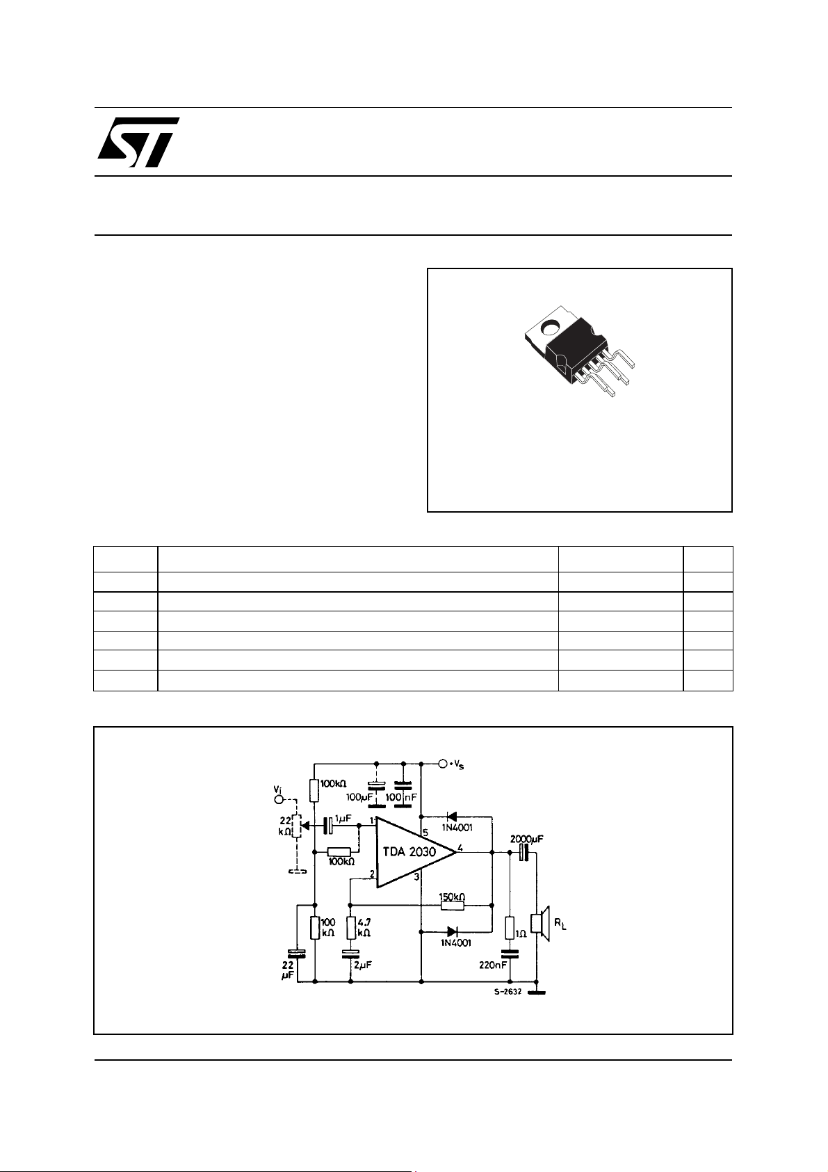
DESCRIPTION
The TDA2030 is a monolithic integrated circuit in
Pentawatt® package, intended for use as a low
frequency class AB amplifier. Typically it provides
14W output power (d = 0.5%) at 14V/4Ω; at ± 14V
or 28V, the guaranteed out put power is 12W on a
4Ω load and 8W on a 8Ω (DIN45500).
The TDA 2030 provides high output current and has
very low harmonic and cross-over distortion.
Further the device incorporates an original (and
patented) short circuit protection system comprising an arrangement for automatically limiting the
dissipated power so as to keep the working point
of the output transistors within their safe operating
area. A conventional thermal shut-down system is
ORDERING NUMBERS
TDA2030V
also included.
ABSOLUTE MAXIMUM RATINGS
Symbol Parameter Value Unit
V
V
V
I
P
T
stg
Supply voltage
s
Input voltage V
i
Differential input voltage
i
Output peak current (internally limited) 3.5 A
o
Power dissip ation at T
tot
, TjStoprage and junction temperature -40 to 150
case
= 90°C
Pentawatt
: TD A2030H
18 (36)
±
s
15
±
20 W
V
V
C
°
TYPICAL APPLICATION
June 1998
1/12
TDA2030
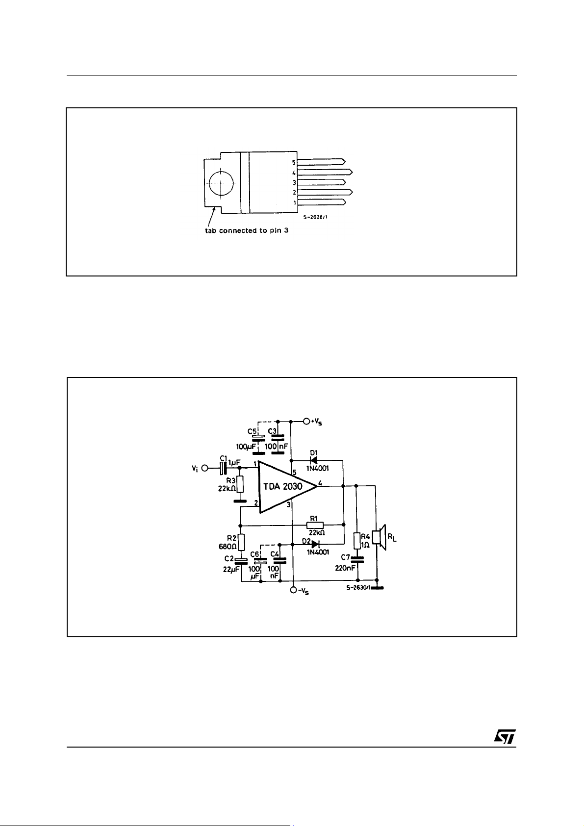
PIN CONNECTION
TEST CIRCUIT
(top view)
+V
S
OUTPUT
-V
S
INVERTING INPUT
NON INVERTING INPUT
2/12
TDA2030
THERMAL DATA
Symbol Parameter Value Unit
R
th j-case
ELECTRICAL CHARACTERISTICS
Thermal resistance junction-case max 3
(Refer to the test circuit, V
= ± 14V , T
s
= 25°C unless otherwise
amb
specified) for single Supply refer to fig. 15 Vs = 28V
Symbol Parameter Test conditions Min. Typ. Max. Unit
V
I
I
V
I
os
P
Supply voltage
s
Quiescent drain current
d
Input bias current 0.2 2
b
Input offset voltage
os
Input offset current
Output power
o
= ± 18V (Vs = 36V)
V
s
d = 0.5% G
f = 40 to 15,000 Hz
R
= 4
Ω
L
R
= 8
Ω
L
d = 10%
G
f = 1 KHz
R
= 4
Ω
L
R
= 8
Ω
L
= 30 dB
v
= 30 dB
v
6
±
12
40 60 mA
2
±
20
±
12
8
14
9
18
11
±
±
±
18
36
20
200
C/W
°
µ
mV
nA
W
W
W
W
V
A
P
d Distortion
= 0.1 to 12W
o
= 4Ω G
R
L
v
f = 40 to 15,000 Hz
= 0.1 to 8W
P
o
= 8Ω G
R
L
v
f = 40 to 15,000 Hz
B Power Bandwidth
(-3 dB)
R
G
G
e
i
Input resistance (pin 1) 0.5 5
i
Voltage gain (open loop) 90 dB
v
Voltage gain (closed loop) f = 1 kHz 29.5 30 30.5 dB
v
Input noise voltage
N
Input noise current 80 200 pA
N
SVR Supply voltage rejection RL = 4Ω G
I
Drain current Po = 14W
d
= 30 dB
G
v
= 12W
P
o
R
L
B = 22 Hz to 22 KHz
R
V
f
ripple
P
g
ripple
o
= 22 k
= W
Ω
= 0.5 V
= 100 Hz
v
eff
R
L
R
L
= 30 dB
= 30 dB
= 4
Ω
= 30 dB
= 4
Ω
= 8
Ω
0.2 0.5 %
0.1 0.5 %
10 to 140,000 Hz
310
40 50
900
500
M
Ω
V
µ
dB
mA
mA
3/12
TDA 2030
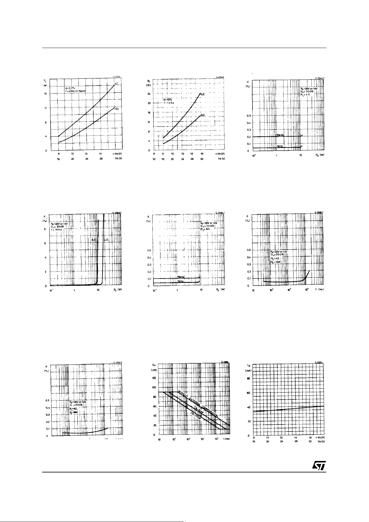
Figure 1. Output power vs.
supply voltage
Figure 4. Distortion vs.
output power
Figure 2. Output power vs.
supply voltage
Figure 5. Distortion vs.
output power
Figure 3. Distortion vs.
output power
Figure 6. Distortion vs.
frequency
Figure 7. Distortion vs.
frequency
4/12
Figure 8. Frequency response with different values
of the rolloff capacitor C8
(see fig. 13)
Figure 9. Quiescent current
vs. supply vo ltage
 Loading...