

现货库存、技术资料、百科信息、热点资讯,精彩尽在鼎好!
DESCRIPTION
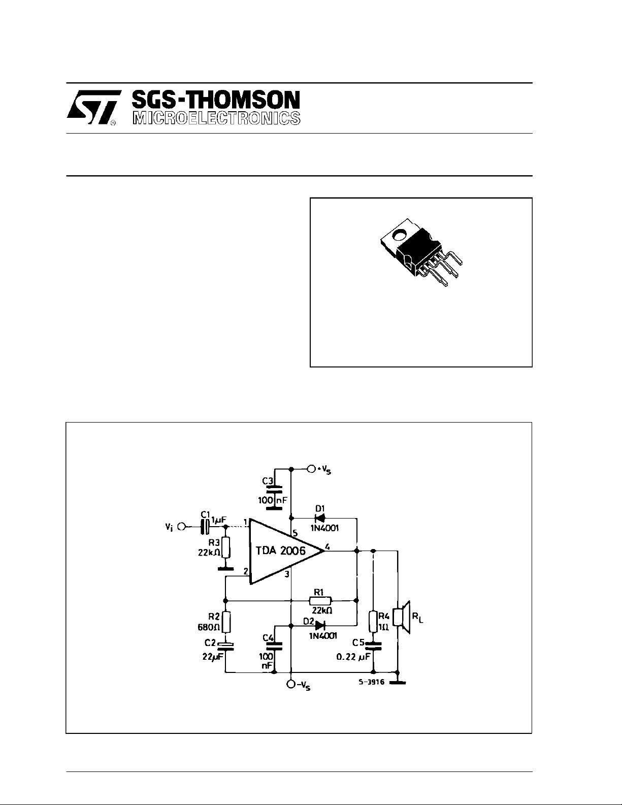
The TDA2006 is a monolithic integrated circuit in
Pentawatt package, intended for use as a low
frequencyclass ”AB” amplifier. At ±12V,d = 10 %
typicallyitprovides12Woutputpowerona4Ω load
and 8W on a 8Ω . The TDA2006 provides high
output current and has very low harmonic and
cross-over distortion. Further the device incorporatesanoriginal(andpatented)shortcircuitprotection system comprising an arrangement for
automaticallylimitingthe dissipatedpower soas to
keep the working point of the output transistors
within their safe operating area. A conventional
thermal shutdown system is also included. The
TDA2006is pin to pin equivalentto theTDA2030.
TDA2006
12W AUDIOAMPLIFIER
PENTAWATT
ORDERING NUMBERS : TDA2006V
TDA2006H
TYPICALAPPLICATION CIRCUIT
May 1995
1/12
TDA2006
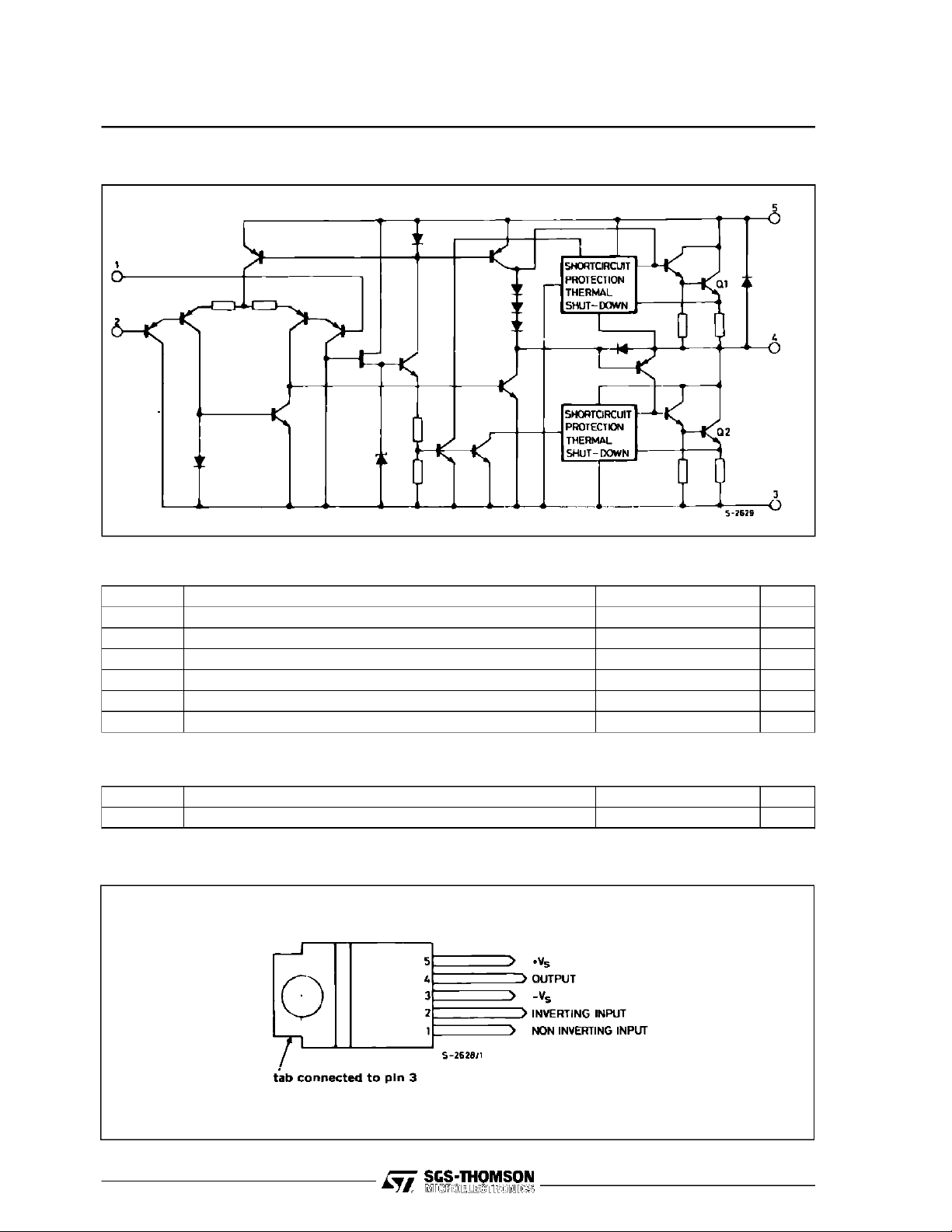
SCHEMATIC DIAGRAM
ABSOLUTE MAXIMUM RATINGS
Symbol Parameter Value Unit
V
s
V
V
I
o
P
tot
T
stg,Tj
Supply Voltage ± 15 V
Input Voltage V
i
Differential Input Voltage ± 12 V
i
s
Output Peak Current (internaly limited) 3 A
Power Dissipation at T
=90°C20W
case
Storage andJunction Temperature – 40 to 150 °C
THERMALDATA
Symbol Parameter Value Unit
R
th (j-c)
Thermal Resistance Junction-case Max 3 °C/W
PIN CONNECTION
2/12

TDA2006
ELECTRICALCHARACTERISTICS
(refer to thetest circuit ; V
= ± 12V, T
S
Symbol Parameter Test Conditions Min. Typ. Max. Unit
V
V
I
V
P
Supply Voltage ± 6 ± 15 V
s
I
Quiescent Drain Current Vs= ± 15V 40 80 mA
d
Input Bias Current Vs= ± 15V 0.2 3 µA
I
b
Input Offset Voltage Vs= ± 15V ± 8mV
OS
Input Offset Current Vs= ± 15V ± 80 nA
OS
Output Offset Voltage Vs= ± 15V ± 10 ± 100 mV
OS
Output Power d = 10%, f = 1kHz
o
d Distortion P
V
Input Sensitivity Po= 10W, RL=4Ω, f = 1kHz
i
B Frequency Response (– 3dB) P
R
Input Resistance (pin1) f = 1kHz 0.5 5 MΩ
i
G
G
e
Voltage Gain (open loop) f = 1kHz 75 dB
v
Voltage Gain (closed loop) f = 1kHz 29.5 30 30.5 dB
v
Input Noise Voltage B (– 3dB) = 22Hz to 22kHz, RL=4Ω 310µV
N
i
Input Noise Current B (– 3dB) = 22Hz to 22kHz, RL=4Ω 80 200 pA
N
SVR Supply Voltage Rejection R
I
Drain Current Po= 12W, RL=4Ω
d
T
Thermal Shutdown Junction
j
Temperature
(*) Referring to Figure 15, single supply.
=25oC unless otherwise specified)
amb
=4Ω
R
L
=8Ω 6
R
L
= 0.1 to 8W, RL=4Ω, f = 1kHz
o
= 0.1 to 4W, RL=8Ω, f = 1kHz
P
o
=6W,RL=8Ω, f = 1kHz
P
o
=8W,RL=4Ω 20Hz to 100kHz
o
=4Ω,Rg= 22kΩ,f
L
=8W,RL=8Ω
P
o
= 100Hz (*) 40 50 dB
ripple
12
8
0.2
0.1
200
220
850
500
145 °C
W
%
%
mV
mV
mA
mA
3/12
TDA2006
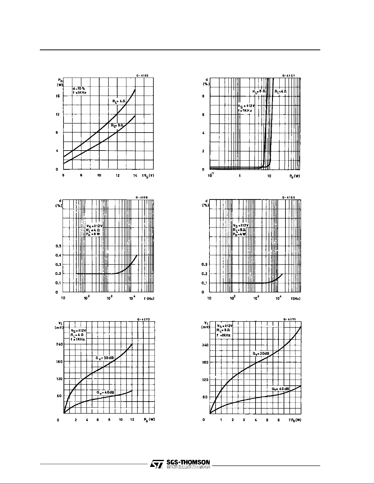
Figure1 : OutputPower versus Supply Voltage Figure 2 : Distortionversus OutputPower
Figure3 : Distortionversus Frequency Figure4 : Distortion versusFrequency
Figure5 : Sensitivityversus Output Power Figure6 : Sensitivityversus OutputPower
4/12

TDA2006
Figure7 : FrequencyResponsewith differentval-
uesof the rolloff CapacitorC8 (see
Figure13)
Figure9 : QuiescentCurrent versus
Supply Voltage
Figure8 : Value of C8 versus Voltage Gain for dif-
ferent Bandwidths (see Figure 13)
Figure10 : Supply Voltage Rejection versus
VoltageGain
Figure11 : PowerDissipationand Efficiency ver-
sus Output Power
Figure12 : Maximum PowerDissipationversus
SupplyVoltage
(sine waveoperation)
5/12

TDA2006
Figure13 : ApplicationCircuit with Spilt PowerSupply
Figure14 : P.C. Board and ComponentsLayoutof theCircuit of Figure 13 (1:1 scale)
6/12

Figure15 : ApplicationCircuit with SinglePower Supply
Figure16 : P.C. Board and ComponentsLayoutof theCircuit of Figure 15 (1:1 scale)
TDA2006
7/12
TDA2006
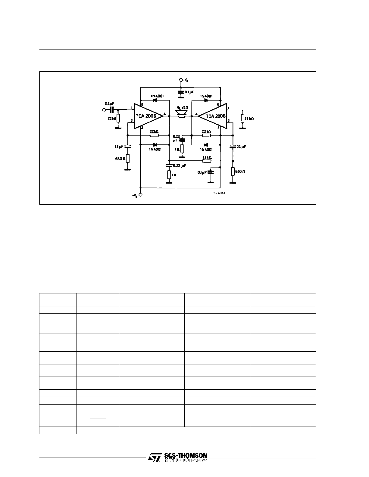
Figure17 : BridgeAmplifierConfiguration with Split PowerSupply(PO= 24W,VS= ± 12V)
PRACTICALCONSIDERATIONS
PrintedCircuit Board
The layout shownin Figure14 should be adopted
by the designers. If different layout are used, the
ground points of input 1 and input 2 must be well
decoupled from ground of the output on which a
ratherhigh current flows.
AssemblySuggestion
No electricalisolationisneededbetween thepack-
age and the heat-sink with single supply voltage
configuration.
ApplicationSuggestion
The recommendedvalues of the components are
the onesshownon applicationcircuitsof Figure13.
Differentvaluescan be used. The table 1 can help
the designers.
Table 1
Component
R
1
R
2
R
3
R
4
R
5
C
1
C
2
C
3C4
C
5C6
C
7
C
8
D
1D2
(*) Closed loop gain must behigher than 24dB.
8/12
Recommanded
Value
22 kΩ Closed Loop GainSetting Increase of Gain Decrease of Gain (*)
680 Ω Closed Loop GainSetting Decrease of Gain (*) Increase of Gain
22 kΩ Non InvertingInput
Biasing
1 Ω Frequency Stability Danger of Oscillation at
3R
2
Upper Frequency Cut-off Poor High Frequencies
2.2 µF Input DC Decoupling Increase of Low
22 µF Inverting Input DC
Decoupling
0.1 µF Supply Voltageby Pass Danger of Oscillation
100 µF Supply Voltage by Pass Danger of Oscillation
0.22 µF Frequency Stability Danger of Oscillation
1
2πBR
1
Upper Frequency Cut-off Lower Bandwidth LargerBandwidth
1N4001 To Protect the Device Against Output Voltage Spikes.
Purpose
Larger Than
Recommanded Value
Increase of Input
Impedance
High Frequencies with
Inductive Loads
Attenuation
Smaller Than
Recommanded Value
Decrease of Input
Impedance
Danger of Oscillation
Frequencies Cut-off
Increase of Low
Frequencies Cut-off

TDA2006
SHORTCIRCUIT PROTECTION
The TDA2006 has an original circuit which limits
the current of the output transistors. Figure 18
shows that the maximumoutput current is a function of the collector emitter voltage ; hence the
output transistors work within their safe operating
area(Figure 19).
Thisfunctioncan thereforebe consideredas being
peak power limiting rather thansimple current limiting.
It reducesthe possibility that the devicegets damaged during an accidental short circuit from AC
output to ground.
THERMALSHUT DOWN
Thepresenceof a thermal limiting circuitoffers the
followingadvantages :
1)an overload on the output (even if it is
permanent), or an above limit ambient
temperaturecan be easily supported since the
cannotbe higherthan 150°C.
T
j
2) the heatsink can have a smallerfactor of safety
compared with that of a conventional circuit.
Thereis no possibilityof device damage due to
high junction temperature.
If for any reason, the junction temperature increasesupto 150°C,thethermalshutdownsimply
reducesthepowerdissipationandthecurrentconsumption.
Figure19 : SafeOperating Area and Collector
Characteristics ofthe Protected
PowerTransistor
Figure20 : OutputPower and DrainCurrent ver-
susCase Temlperature(R
=4Ω)
L
The maximum allowable power dissipation depends upon the size of the external heatsink (i.e.
its thermalresistance) ; Figure22 shows the dissipablepower as a function of ambient temperature
for differentthermal resistances.
Figure18 : MaximumOutput Current versus
VoltageV
accross each Out-
CE (sat)
put Transistor
Figure21 : OutputPower and DrainCurrent ver-
susCase Temlperature(R
=8Ω)
L
9/12

TDA2006
Figure22 : MaximumAllowable PowerDissipa-
tion versusAmbientTemperature
DIMENSIONSUGGESTION
Thefollowingtable showsthelengthoftheheatsink
in Figure23 for severalvalues of P
P
(W) 12 8 6
tot
Lenght of Heatsink (mm) 60 40 30
R
of Heatsink (°C/W) 4.2 6.2 8.3
th
andRth.
tot
Figure 23 : Example of Heatsink
10/12

PENTAWATT PACKAGE MECHANICAL DATA
TDA2006
DIM.
MIN. TYP. MAX. MIN. TYP. MAX.
mm inch
A 4.8 0.189
C 1.37 0.054
D 2.4 2.8 0.094 0.110
D1 1.2 1.35 0.047 0.053
E 0.35 0.55 0.014 0.022
F 0.8 1.05 0.031 0.041
F1 1 1.4 0.039 0.055
G 3.4 0.126 0.134 0.142
G1 6.8 0.260 0.268 0.276
H2 10.4 0.409
H3 10.05 10.4 0.396 0.409
L 17.85 0.703
L1 15.75 0.620
L2 21.4 0.843
L3 22.5 0.886
L5 2.6 3 0.102 0.118
L6 15.1 15.8 0.594 0.622
L7 6 6.6 0.236 0.260
M 4.5 0.177
M1 4 0.157
Dia 3.65 3.85 0.144 0.152
A
H3
L
L1
C
D1
L5
Dia.
L7
L6
L2
L3
D
F1
H2
E
MM1
G1
G
F
11/12

TDA2006
Information furnished is believed to be accurate andreliable. However,SGS-THOMSON Microelectronicsassumes no responsibility
for the consequences of use of such information nor for anyinfringement ofpatents or other rights of third parties which may result
from its use. No license is granted byimplication orotherwise under any patent or patent rights of SGS-THOMSON Microelectronics.
Specifications mentioned in this publication are subject to change without notice. This publication supersedes and replaces all
information previously supplied. SGS-THOMSON Microelectronics products arenot authorized for use as critical components in life
support devices or systems without express written approval of SGS-THOMSON Microelectronics.
1995 SGS-THOMSON Microelectronics - AllRights Reserved
PENTAWATT is Registered Trademarkof SGS-THOMSON Microelectronics
Australia- Brazil - France - Germany- Hong Kong - Italy - Japan - Korea - Malaysia - Malta - Morocco - The Netherlands - Singa-
pore - Spain - Sweden - Switzerland - Taiwan - Thaliand - United Kingdom - U.S.A.
SGS-THOMSON Microelectronics GROUP OF COMPANIES
12/12
 Loading...