

Page 1

10 + 10 W stereo amplifier for car radio
Features
■ Low distortion
■ Low noise
■ Protection against:
– Output AC short circuit to ground
– Overrating chip temperature
– Load dump voltage surge
– Fortuitous open ground
– Very inductive loads
Description
The TDA2004R is a class B dual audio power
amplifier in Multiwatt11 package specifically
designed for car radio applications.
Table 1. Device summary
TDA2004R
Multiwatt11
Power booster amplifiers can be easily designed
using this device that provides a high current
capability (up to 3.5 A) and can drive very low
impedance loads (down to 1.6 Ω).
The TDA2004R allows very compact applications
because few external components are required
and it doesn't need electrical insulation between
the package and the heatsink.
Order code Package Packing
TDA2004R Multiwatt11 Tube
June 2010 Doc ID 17614 Rev 1 1/17
www.st.com
1
Page 2

Contents TDA2004R
Contents
1 Pins description . . . . . . . . . . . . . . . . . . . . . . . . . . . . . . . . . . . . . . . . . . . . 5
2 Electrical specifications . . . . . . . . . . . . . . . . . . . . . . . . . . . . . . . . . . . . . . 6
2.1 Absolute maximum ratings . . . . . . . . . . . . . . . . . . . . . . . . . . . . . . . . . . . . . 6
2.2 Thermal data . . . . . . . . . . . . . . . . . . . . . . . . . . . . . . . . . . . . . . . . . . . . . . . 6
2.3 Electrical characteristics . . . . . . . . . . . . . . . . . . . . . . . . . . . . . . . . . . . . . . . 6
2.4 Test and application circuit . . . . . . . . . . . . . . . . . . . . . . . . . . . . . . . . . . . . . 8
2.5 Electrical characteristics curves . . . . . . . . . . . . . . . . . . . . . . . . . . . . . . . . . 9
3 Application suggestion . . . . . . . . . . . . . . . . . . . . . . . . . . . . . . . . . . . . . . 12
3.1 Built-in protection systems . . . . . . . . . . . . . . . . . . . . . . . . . . . . . . . . . . . . 12
3.1.1 Load dump voltage surge . . . . . . . . . . . . . . . . . . . . . . . . . . . . . . . . . . . 12
3.1.2 Short circuit (AC condition) . . . . . . . . . . . . . . . . . . . . . . . . . . . . . . . . . . 13
3.1.3 Polarity inversion . . . . . . . . . . . . . . . . . . . . . . . . . . . . . . . . . . . . . . . . . . 13
3.1.4 Open ground . . . . . . . . . . . . . . . . . . . . . . . . . . . . . . . . . . . . . . . . . . . . . 13
3.1.5 Inductive load . . . . . . . . . . . . . . . . . . . . . . . . . . . . . . . . . . . . . . . . . . . . . 13
3.1.6 DC voltage . . . . . . . . . . . . . . . . . . . . . . . . . . . . . . . . . . . . . . . . . . . . . . . 13
3.1.7 Thermal shut-down . . . . . . . . . . . . . . . . . . . . . . . . . . . . . . . . . . . . . . . . 14
4 Package information . . . . . . . . . . . . . . . . . . . . . . . . . . . . . . . . . . . . . . . . 15
5 Revision history . . . . . . . . . . . . . . . . . . . . . . . . . . . . . . . . . . . . . . . . . . . 16
2/17 Doc ID 17614 Rev 1
Page 3

TDA2004R List of tables
List of tables
Table 1. Device summary . . . . . . . . . . . . . . . . . . . . . . . . . . . . . . . . . . . . . . . . . . . . . . . . . . . . . . . . . . 1
Table 2. Absolute maximum ratings . . . . . . . . . . . . . . . . . . . . . . . . . . . . . . . . . . . . . . . . . . . . . . . . . . 6
Table 3. Thermal data. . . . . . . . . . . . . . . . . . . . . . . . . . . . . . . . . . . . . . . . . . . . . . . . . . . . . . . . . . . . . 6
Table 4. Electrical characteristics . . . . . . . . . . . . . . . . . . . . . . . . . . . . . . . . . . . . . . . . . . . . . . . . . . . . 6
Table 5. Recommended values of the component of the application circuit. . . . . . . . . . . . . . . . . . . 12
Table 6. Document revision history . . . . . . . . . . . . . . . . . . . . . . . . . . . . . . . . . . . . . . . . . . . . . . . . . 16
Doc ID 17614 Rev 1 3/17
Page 4

List of figures TDA2004R
List of figures
Figure 1. Pins connection diagram (top view) . . . . . . . . . . . . . . . . . . . . . . . . . . . . . . . . . . . . . . . . . . . 5
Figure 2. Test and application circuit . . . . . . . . . . . . . . . . . . . . . . . . . . . . . . . . . . . . . . . . . . . . . . . . . . 8
Figure 3. Printed circuit board and components layout of the figure 2. . . . . . . . . . . . . . . . . . . . . . . . . 8
Figure 4. Quiescent output voltage vs. supply voltage . . . . . . . . . . . . . . . . . . . . . . . . . . . . . . . . . . . . 9
Figure 5. Quiescent drain current vs. supply voltage . . . . . . . . . . . . . . . . . . . . . . . . . . . . . . . . . . . . . . 9
Figure 6. Distortion vs. output power . . . . . . . . . . . . . . . . . . . . . . . . . . . . . . . . . . . . . . . . . . . . . . . . . . 9
Figure 7. Output power vs. supply voltage, R
Figure 8. Output power vs. supply voltage, R
Figure 9. Distortion vs. frequency, R
Figure 10. Distortion vs. frequency, R
= 2 and 4 Ω . . . . . . . . . . . . . . . . . . . . . . . . . . . . . . . . . . . . . . . . . . . .9
L
= 1.6 and 3.2 Ω . . . . . . . . . . . . . . . . . . . . . . . . . . . . . . . . . . . . . . . .10
L
Figure 11. Supply voltage rejection vs. C3 . . . . . . . . . . . . . . . . . . . . . . . . . . . . . . . . . . . . . . . . . . . . . 10
Figure 12. Supply voltage rejection vs. frequency . . . . . . . . . . . . . . . . . . . . . . . . . . . . . . . . . . . . . . . . 10
Figure 13. Supply voltage rejection vs. C2 and C3, G
Figure 14. Supply voltage rejection vs. C2 and C3, G
Figure 15. Gain vs. input sensitivity . . . . . . . . . . . . . . . . . . . . . . . . . . . . . . . . . . . . . . . . . . . . . . . . . . . 10
Figure 16. Total power dissipation and efficiency vs. output power (R
Figure 17. Total power dissipation and efficiency vs. output power (R
Figure 18. Maximum allowable power dissipation vs. ambient temperature . . . . . . . . . . . . . . . . . . . . 11
Figure 19. Suggested LC network circuit . . . . . . . . . . . . . . . . . . . . . . . . . . . . . . . . . . . . . . . . . . . . . . . 13
Figure 20. Voltage gain bridge configuration . . . . . . . . . . . . . . . . . . . . . . . . . . . . . . . . . . . . . . . . . . . . 13
Figure 21. Multiwatt11 mechanical data and package dimensions . . . . . . . . . . . . . . . . . . . . . . . . . . . 15
= 2 and 4 Ω . . . . . . . . . . . . . . . . . . . . . . . . . . . . . . . . . . . . .9
L
= 1.6 and 3.2Ω . . . . . . . . . . . . . . . . . . . . . . . . . . . . . . . . . .9
L
= 390/1Ω. . . . . . . . . . . . . . . . . . . . . . . . . . . . . . . .10
V
= 1000/10Ω . . . . . . . . . . . . . . . . . . . . . . . . . . . . .10
V
= 2 Ω) . . . . . . . . . . . . . . . . . . 11
L
= 3.2 Ω ) . . . . . . . . . . . . . . . . 11
L
4/17 Doc ID 17614 Rev 1
Page 5

TDA2004R Pins description
1 Pins description
Figure 1. Pins connection diagram (top view)
TAB CONNECTED TO PIN 6
11
10
9
8
7
6
5
4
3
2
1
D95AU318
BOOTSTRAP(1)
OUTPUT(1)
+V
S
OUTPUT(2)
BOOTSTRAP(2)
GND
INPUT+(2)
INPUT-(2)
SVRR
INPUT-(1)
INPUT+(1)
Doc ID 17614 Rev 1 5/17
Page 6

Electrical specifications TDA2004R
2 Electrical specifications
2.1 Absolute maximum ratings
Table 2. Absolute maximum ratings
Symbol Parameter Value Unit
Operating supply voltage 18
V
S
Peak supply voltage (50 ms) 40
VDC supply voltage 28
(1)
Io
Output peak current (non repetitive t = 0.1 ms) 4.5
Output peak current (repetitive f ≥10 Hz) 3.5
P
tot
T
, T
stg
1. The max. output current is internally limited.
Power dissipation at T
Storage and junction temperature -40 to 150 °C
j
= 60 °C 30 W
case
2.2 Thermal data
Table 3. Thermal data
Symbol Parameter Value Unit
R
th-j-case
Thermal resistance junction-to-case max 3 °C/W
2.3 Electrical characteristics
Refer to the stereo application circuit T
otherwise specified
Table 4. Electrical characteristics
Symbol Parameter Test condition Min. Typ. Max. Unit
= 25 °C; Gv = 50 dB; R
amb
th(heatsink)
= 4 °C/W unless
A
V
V
Supply voltage 8 18 V
S
V
= 14.4 V
Quiescent offset voltage
o
I
Total quiescent drain current
d
S
= 13.2 V
V
S
V
= 14.4 V
S
= 13.2 V
V
S
f = 1 kHz; THD = 10 %
= 14.4 V; RL = 4 Ω
V
S
P
Output power (each channel)
o
= 14.4 V; RL = 3.2 Ω
V
S
VS = 14.4 V; RL = 2 Ω
= 14.4 V; RL = 1.6 Ω
V
S
6/17 Doc ID 17614 Rev 1
6.6
6
6
7
9
10
7.2
6.6
-
65
62
7.8
7.2
120
120
V
V
mA
mA
6.5
8
-W
10
11
Page 7

TDA2004R Electrical specifications
Table 4. Electrical characteristics (continued)
Symbol Parameter Test condition Min. Typ. Max. Unit
f = 1 kHz; THD = 10 %
P
Output power (each channel)
o
VS = 13.2 V; RL =3.2 Ω
= 13.2 V; RL = 1.6 Ω
V
S
6
9
VS = 16 V; RL = 2 Ω
10
6.5
12
(1)
-W
THD Total harmonic distortion
CT Cross talk
Input saturation voltage - 300 - mW
V
i
R
f
Input resistance f = 1 kHz 70 200 - kΩ
i
f
Low frequency roll off (-3 dB)
L
High frequency roll off (-3 dB) RL = 1.6 Ω to 4 Ω 15 - - kHz
H
Open loop voltage gain f = 1 kHz - 90 -
G
v
Closed loop voltage gain f = 1 kHz 48 50 51
ΔG
e
Closed loop gain matching - - 0.5 - dB
v
Total input noise voltage Rg = 10 kΩ
N
SVR Supply voltage rejection
η Efficiency
T
Thermal shutdown junction
J
temperature
f = 1 kHz; V
RL = 4 Ω; Po = 50 mW to 4 W;
f = 1 kHz; V
RL = 2 Ω; Po = 50 mW to 6 W;
f = 1 kHz; V
RL = 3.2 Ω; Po = 50 mW to 3W;
f = 1KHz; V
RL = 1.6Ω; Po = 40mW to 6W;
V
= 14.4 V; Vo = 4 V
S
= 5 kΩ; RL = 4 Ω;
R
g
f = 1 kHz
f = 10 kHz
R
= 4 Ω
L
= 2 Ω
R
L
RL = 3.2 Ω
= 1.6 Ω
R
L
= 14.4 V;
S
= 14.4 V;
S
= 13.2 V;
S
= 13.2V;
S
RMS
-0.21%
-0.31%
-0.21%
-0.31%
;
50
40
60
45
-
mW
mW
35
--
50
40
Hz
55
dB
(2)
-1.55μV
V
= 0.5 Vrms;
ripple
=100 Hz; Rg = 10 kΩ;
f
ripple
= 10 μF
C
3
f = 1 kHz; V
= 14.4 V;
S
RL = 4 Ω; Po = 6.5 W;
= 2Ω; Po = 10 W;
R
L
f = 1 kHz; V
= 3.2 Ω; Po = 6.5 W;
R
L
= 1.6 Ω; Po = 10 W;
R
L
= 13.2 V;
S
35 45 - dB
-7060-%
-7060-%
- - 145 - °C
1. 9.3 W without bootstrap.
2. Bandwidth filter: 22 Hz to 22 kHz.
Doc ID 17614 Rev 1 7/17
Page 8

Electrical specifications TDA2004R
2.4 Test and application circuit
Figure 2. Test and application circuit
+V
s
0.1µF
120 kΩ
C12
93
C3
10 µF
INPUT (L)
INPUT (R)
2.2µF
5
3V 1/2
C1
2.2µF
1
3V
C2
+
TDA 2004R
–
+
1/2
TDA 2004R
–
6
7
8
4
11
10
2
C4
1.2 kΩ
220 µF
C5
C6
1.2 kΩ
220 µF
C7
33 Ω
33 Ω
100 µF
10 V
100 µF
10 V
R3
R5
R6
R7
2200 µF
C8R2
0.1 µF
1 Ω
2200 µF
C9R4
0.1 µF
1 Ω
Figure 3. Printed circuit board and components layout of the figure 2
10 V
C10
10 V
C11
R
L
R
L
8/17 Doc ID 17614 Rev 1
Page 9
TDA2004R Electrical specifications
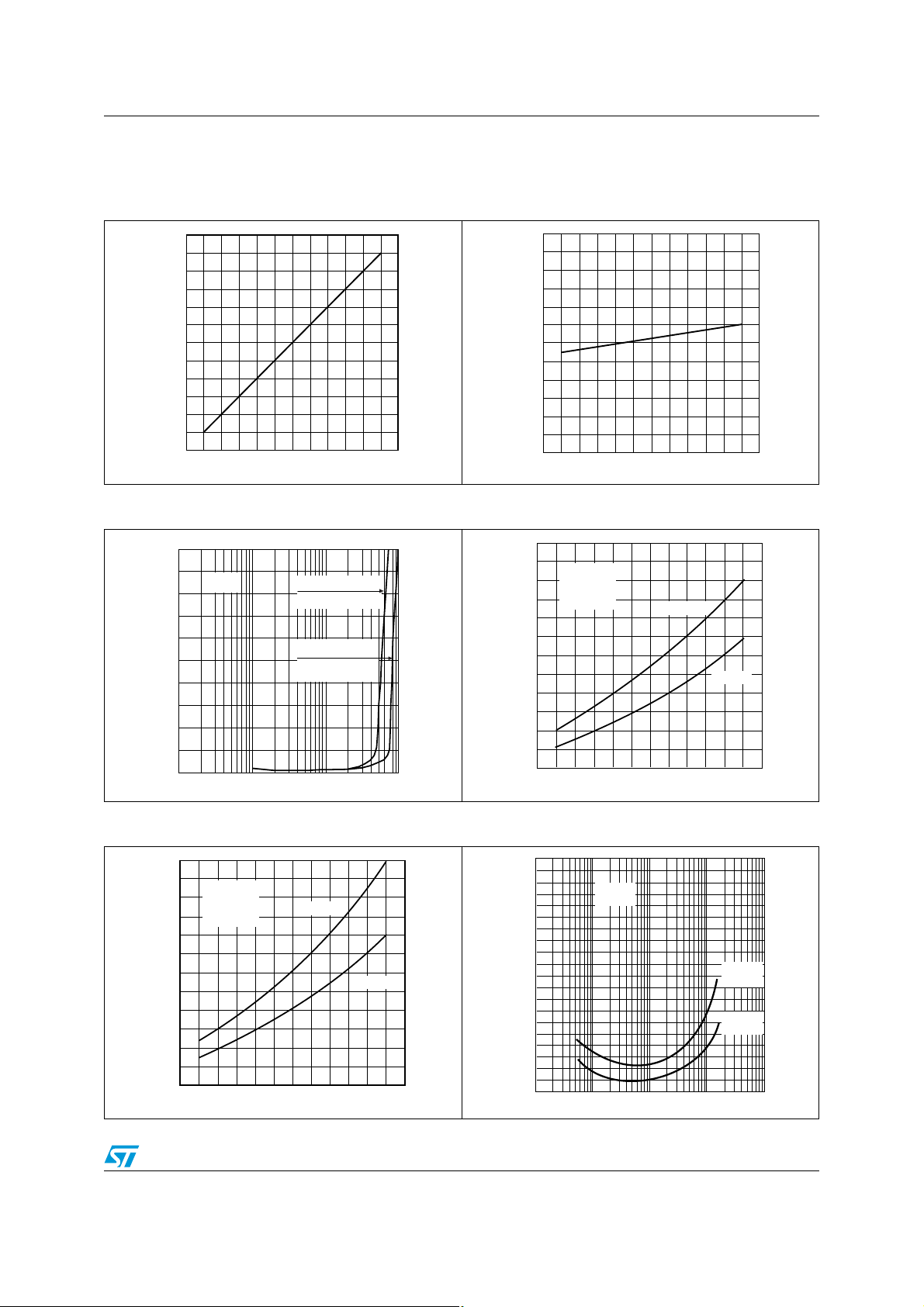
2.5 Electrical characteristics curves
Figure 4. Quiescent output voltage vs. sup-
ply voltage
V
O
(V)
8
7
6
5
4
08
10 12 14 16 Vs (V)
Figure 5. Quiescent drain current vs. supply
voltage
I
d
(mA)
100
80
60
40
20
08
10 12 14 16 Vs (V)
Figure 6. Distortion vs. output power Figure 7. Output power vs. supply voltage,
R
= 2 and 4 Ω
(%)
d
f = 1 kHz
Gv = 50 dB
8
6
4
Vs = 13.2 V
Vs = 14.4 V
Vs = 13.2 V
Vs = 14.4 V
R
R
L
R
L
R
= 3.2 Ω
= 4 Ω
L
= 1.6 Ω
= 2 Ω
L
P
(W)
15
12
L
o
f = 1 kHz
G
v = 50 dB
d = 10 %
9
6
RL = 2 Ω
RL = 4 Ω
2
0
0.01 0.1 1 Po (W)
Figure 8. Output power vs. supply voltage,
R
= 1.6 and 3.2Ω
P
(W)
15
12
L
o
f = 1 kHz
G
v = 50 dB
d = 10 %
9
RL = 1.6 Ω
RL = 3.2 Ω
6
3
0
8
10
12
14 16
Vs (V)
Doc ID 17614 Rev 1 9/17
3
0
8
10
12
14 16
Figure 9. Distortion vs. frequency, R
4 Ω
d
(%)
= 14.4 V
V
s
Gv = 50 dB
1.2
P
o
R
= 2 Ω
L
0.8
P
o
R
= 4 Ω
L
0.4
10
2
10
3
10
4
10
Vs (V)
= 2 and
L
= 2.5 W
= 2.5 W
f (Hz)
Page 10

Electrical specifications TDA2004R
Figure 10. Distortion vs. frequency, RL = 1.6
and 3.2 Ω
(%)
1.2
0.8
0.4
d
V
= 13.2 V
s
Gv = 50 dB
= 2.5 W
P
o
R
= 1.6 Ω
L
= 2.5 W
P
o
R
= 3.2 Ω
L
10
2
10
3
10
4
f (Hz)
10
Figure 12. Supply voltage rejection vs.
frequency
SVR
(dB)
Vs = 14.4 V
Gv = 50 dB
= 10 µF
C
3
60
50
40
30
20
Rg = 0
Rg = 10 kΩ
Figure 11. Supply voltage rejection vs. C3
SVR
(dB)
10
20
30
40
50
60
Vs = 14.4 V
f
= 100 kHz
ripple
= 0.5 V
V
ripple
Gv = 50 dB
= 10 kΩ
R
g
10 12 C
(µF)13
3
Figure 13. Supply voltage rejection vs. C2 and
SVR
(dB)
50
40
30
C3, G
Vs = 14.4 V
R
= 4 Ω
L
R
= 10 kΩ
g
Gv = 390/1 Ω
f
ripple
= 100 Hz
= 390/1Ω
V
C2 = 220 µF
C2 = 22 µF
C2 = 5 µF
10 10
2
Figure 14. Supply voltage rejection vs. C2 and
3
10
f (Hz)
Figure 15. Gain vs. input sensitivity
C3, GV = 1000/10Ω
10/17 Doc ID 17614 Rev 1
SVR
(dB)
50
40
30
20
Vs = 14.4 V
R
= 4 Ω
L
= 10 kΩ
R
g
Gv = 1000/10 Ω
= 100 Hz
f
ripple
C2 = 220 µF
C2 = 22 µF
C2 = 5 µF
10 20 C
(dB)
46
(µF)12 5
3
20
G
v
54
50
42
Po = 6 W
38
34
Po = 0.5 W
30
26
22
2468 2468
10 100
30
10 20 C
VS = 14.4 V
f = 1 kHz
R
= 4 Ω
L
300 V
(mV)
i
(µF)12 5
3
G
v
500
200
100
50
20
Page 11
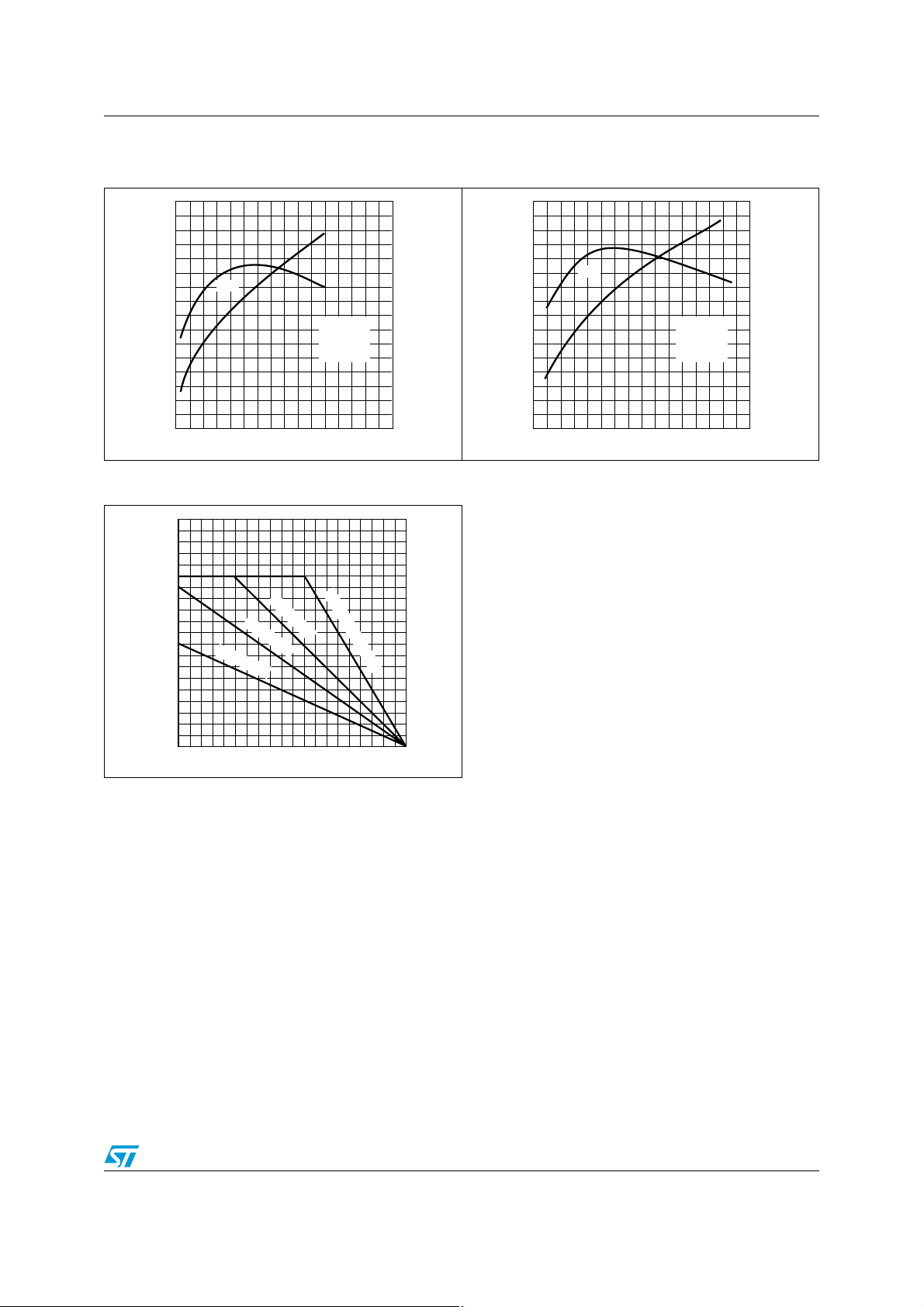
TDA2004R Electrical specifications
Figure 16. Total power dissipation and
efficiency vs. output power (R
P
(W)
tot
12
P
10
8
6
4
2
tot
η
Vs = 14.4 V
R
= 4 Ω
L
f = 1 kHz
Gv = 50 dB
20 24 P
= 2Ω)
L
η
(%)
60
40
20
(W)841216
o
Figure 18. Maximum allowable power dissipa-
tion vs. ambient temperature
P
(W)
32
28
24
20
16
12
8
4
0
tot
= 2˚C/W
50
INFINITE HEATSINK
100 T
amb
(˚C)
-50
R
th
= 8˚C/W
0
R
th
= 4˚C/W
R
th
Figure 17. Total power dissipation and efficiency
vs. output power (R
P
tot
(W)
6
4
2
P
tot
η
= 3.2 Ω)
L
Vs = 13.2 V
R
= 3.2 Ω
L
f = 1 kHz
Gv = 50 dB
10 12 P
η
(%)
60
40
20
(W)4268
o
Doc ID 17614 Rev 1 11/17
Page 12

Application suggestion TDA2004R
3 Application suggestion
The recommended values of the components are those shown on application circuit of
Figure 2. Different values can be used; the following table can help the designer.
Table 5. Recommended values of the component of the application circuit
Component
R1 120 kΩ
R2, R4 1 kΩ
R3, R5 3.3 Ω Decrease of gain Increase of gain
R6, R7 1 Ω Frequency stability
C1, C2 2.2 μF Input DC decoupling High turn-on delay
C3 10 μF Ripple rejection
C4, C6 100 μF Bootstrapping -
C5, C7 100 μF
C8, C9 0.1 μF Frequency stability - Danger of oscillation
C10, C11 1000 to 2200 μF Output DC decoupling -
1. The closed loop gain must be higher than 26 dB.
Recommended
value
Purpose Larger than Smaller than r
Optimization of the
output signal symmetry
Closed loop gain setting
(1)
Feedback input DC
decoupling
Smaller P
Increase of gain Decrease of gain
Danger of oscillation
at high frequency with
inductive load
Increase of SVR,
Increase of the switch-on
time
--
omax
Smaller P
High turn-on pop, higher
low frequency cutoff.
Increase of noise
Degradation of SVR
Increase of distortion at
low frequency
Higher low-frequency
cut-off
omax
3.1 Built-in protection systems
3.1.1 Load dump voltage surge
The TDA2004R has a circuit which enables it to withstand voltage pulse train, on Pin 9, of
the type shown in Figure 20. If the supply voltage peaks to more than 40 V, then an LC filter
must be inserted between the supply and pin 9, in order to assure that the pulses at pin 9
will be held within the limits shown.
A suggested LC network is shown in Figure 19. With this network, a train of pulses with
amplitude up to 120 V and width of 2 ms can be applied at point A. This type of protection is
ON when the supply voltage (pulse or DC) exceeds 18 V. For this reason the maximum
operating supply voltage is 18 V.
12/17 Doc ID 17614 Rev 1
Page 13

TDA2004R Application suggestion
Figure 19. Suggested LC network circuit
L = 2mH
FROM
SUPPLY
LINE
A
TO PIN
C
3000 µF
16V
Figure 20. Voltage gain bridge configuration
Vs (V)
40
t1 = 50ms
t2 = 1000ms
14.4
t1
t2
t
3.1.2 Short circuit (AC condition)
The TDA2004R can withstand a permanent short-circuit from the output to ground caused
by a wrong connection during normal working.
3.1.3 Polarity inversion
High current (up to 10 A) can be handled by the device with no damage for a longer period
than the blow-out time of a quick 2 A fuse (normally connected in series with the supply).
This feature is added to avoid destruction, if during fitting to the car, a mistake on the
connection of the supply is made.
3.1.4 Open ground
When the ratio is in the ON condition and the ground is accidentally opened, a standard
audio amplifier will be damaged. On the TDA2004R protection diodes are included to avoid
any damage.
3.1.5 Inductive load
A protection diode is provided to allow use of the TDA2004R with inductive loads.
3.1.6 DC voltage
The maximum operating DC voltage for the TDA2004R is 18 V. However the device can
withstand a DC voltage up to 28 V with no damage. This could occur during winter if two
batteries are series connected to crank the engine.
Doc ID 17614 Rev 1 13/17
Page 14

Application suggestion TDA2004R
3.1.7 Thermal shut-down
The presence of a thermal limiting circuit offers the following advantages:
1. an overload on the output (even if it is permanent), or an excessive ambient
temperature can be easily withstood.
2. the heatsink can have a smaller factor of safety compared with that of a conventional
circuit. There is no device damage in the case of excessive junction temperature: all
that happens is that P
The maximum allowable power dissipation depends upon the size of the external heatsink
(i.e. its thermal resistance); Figure 18 shows the power dissipation as a function of ambient
temperature for different thermal resistance.
(and therefore P
o
) and Id are reduced.
tot
14/17 Doc ID 17614 Rev 1
Page 15
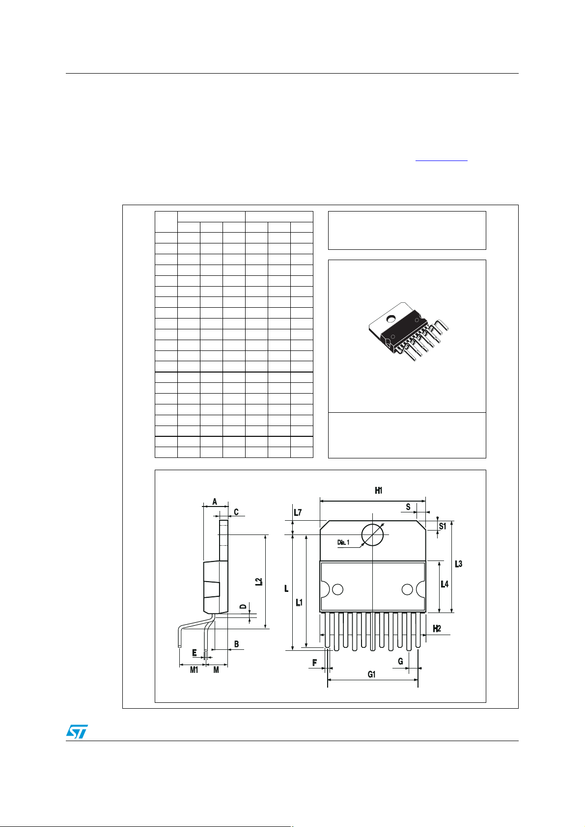
TDA2004R Package information
4 Package information
In order to meet environmental requirements, ST offers these devices in different grades of
ECOPACK
®
packages, depending on their level of environmental compliance. ECOPACK
®
specifications, grade definitions and product status are available at: www.st.com.
ECOPACK
®
is an ST trademark.
Figure 21. Multiwatt11 mechanical data and package dimensions
DIM.
A50.197
B 2.65 0.104
C1.60.063
D 1 0.039
E 0.49 0.55 0.019 0.022
F 0.88 0.95 0.035 0.037
G 1.45 1.7 1.95 0.057 0.067 0.0 77
G1 16.75 17 17.25 0.659 0.669 0.679
H1 19.6 0.772
H2 20.2 0.795
L 21.9 22.2 22.5 0.862 0.874 0.886
L1 21.7 22.1 22.5 0.854 0.87 0.886
L2 17.4 18.1 0.685 0.713
L3 17.25 17.5 17.75 0.679 0.689 0.699
L4 10.3 10.7 10.9 0.406 0.421 0.429
L7 2.65 2.9 0.104 0.114
M 4.25 4.55 4.85 0.167 0.179 0.191
M1 4.73 5.08 5.43 0.186 0.200 0.214
S 1.9 2.6 0.075 0.102
S1 1.9 2.6 0.075 0.102
Dia1 3.65 3.85 0.144 0.152
mm inch
MIN. TYP. MAX. MIN. TYP. MAX.
OUTLINE AND
MECHANICAL DATA
Multiwatt11 (Vertical)
0016035 H
Doc ID 17614 Rev 1 15/17
Page 16

Revision history TDA2004R
5 Revision history
Table 6. Document revision history
Date Revision Changes
18-Jun-2010 1 Initial release.
16/17 Doc ID 17614 Rev 1
Page 17

TDA2004R
Please Read Carefully:
Information in this document is provided solely in connection with ST products. STMicroelectronics NV and its subsidiaries (“ST”) reserve the
right to make changes, corrections, modifications or improvements, to this document, and the products and services described herein at any
time, without notice.
All ST products are sold pursuant to ST’s terms and conditions of sale.
Purchasers are solely responsible for the choice, selection and use of the ST products and services described herein, and ST assumes no
liability whatsoever relating to the choice, selection or use of the ST products and services described herein.
No license, express or implied, by estoppel or otherwise, to any intellectual property rights is granted under this document. If any part of this
document refers to any third party products or services it shall not be deemed a license grant by ST for the use of such third party products
or services, or any intellectual property contained therein or considered as a warranty covering the use in any manner whatsoever of such
third party products or services or any intellectual property contained therein.
UNLESS OTHERWISE SET FORTH IN ST’S TERMS AND CONDITIONS OF SALE ST DISCLAIMS ANY EXPRESS OR IMPLIED
WARRANTY WITH RESPECT TO THE USE AND/OR SALE OF ST PRODUCTS INCLUDING WITHOUT LIMITATION IMPLIED
WARRANTIES OF MERCHANTABILITY, FITNESS FOR A PARTICULAR PURPOSE (AND THEIR EQUIVALENTS UNDER THE LAWS
OF ANY JURISDICTION), OR INFRINGEMENT OF ANY PATENT, COPYRIGHT OR OTHER INTELLECTUAL PROPERTY RIGHT.
UNLESS EXPRESSLY APPROVED IN WRITING BY AN AUTHORIZED ST REPRESENTATIVE, ST PRODUCTS ARE NOT
RECOMMENDED, AUTHORIZED OR WARRANTED FOR USE IN MILITARY, AIR CRAFT, SPACE, LIFE SAVING, OR LIFE SUSTAINING
APPLICATIONS, NOR IN PRODUCTS OR SYSTEMS WHERE FAILURE OR MALFUNCTION MAY RESULT IN PERSONAL INJURY,
DEATH, OR SEVERE PROPERTY OR ENVIRONMENTAL DAMAGE. ST PRODUCTS WHICH ARE NOT SPECIFIED AS "AUTOMOTIVE
GRADE" MAY ONLY BE USED IN AUTOMOTIVE APPLICATIONS AT USER’S OWN RISK.
Resale of ST products with provisions different from the statements and/or technical features set forth in this document shall immediately void
any warranty granted by ST for the ST product or service described herein and shall not create or extend in any manner whatsoever, any
liability of ST.
ST and the ST logo are trademarks or registered trademarks of ST in various countries.
Information in this document supersedes and replaces all information previously supplied.
The ST logo is a registered trademark of STMicroelectronics. All other names are the property of their respective owners.
© 2010 STMicroelectronics - All rights reserved
STMicroelectronics group of companies
Australia - Belgium - Brazil - Canada - China - Czech Republic - Finland - France - Germany - Hong Kong - India - Israel - Italy - Japan -
Malaysia - Malta - Morocco - Philippines - Singapore - Spain - Sweden - Switzerland - United Kingdom - United States of America
www.st.com
Doc ID 17614 Rev 1 17/17
 Loading...