

y
TD310
TRIPLE IGBT/MOS DRIVER WITH CURRENT SENSE
■ THREE POWER IGBT/MOS AND PULSE
TRANSFORMER DRIVERS
■ CURRENT SENSE COMPARATOR
■ UNCOMMITTED OP-AMP
■ 0.6 A PER CHANNEL PEAK OUTPUT
CURRENT CAPABILITY
■ LOW OUTPUT IMPEDANCE TYP: 7Ω AT
200mA
■ CMOS/LSTTL COMPATIBLE INVERTING
INPUT WITH HYSTERESIS
■ 4V TO 16V SINGLE SUPPLY OPERATION
■ LOW BIAS CURRENT TYP: 1.5mA
■ ADJUSTABLE UNDERVOLTAGE LOCKOUT
LEVEL
■ STAND-BY MODE
■ CHANNE L PARALLELING CAPABI LITY
DESCRIPTION
The TD310 is designed t o drive one, two or th ree
Power IGBT/MOS and has driving capability for
pulse transformer. So it is perfectly suited to
interface control IC with Power Switches in low
side or half-b ridge config uration.
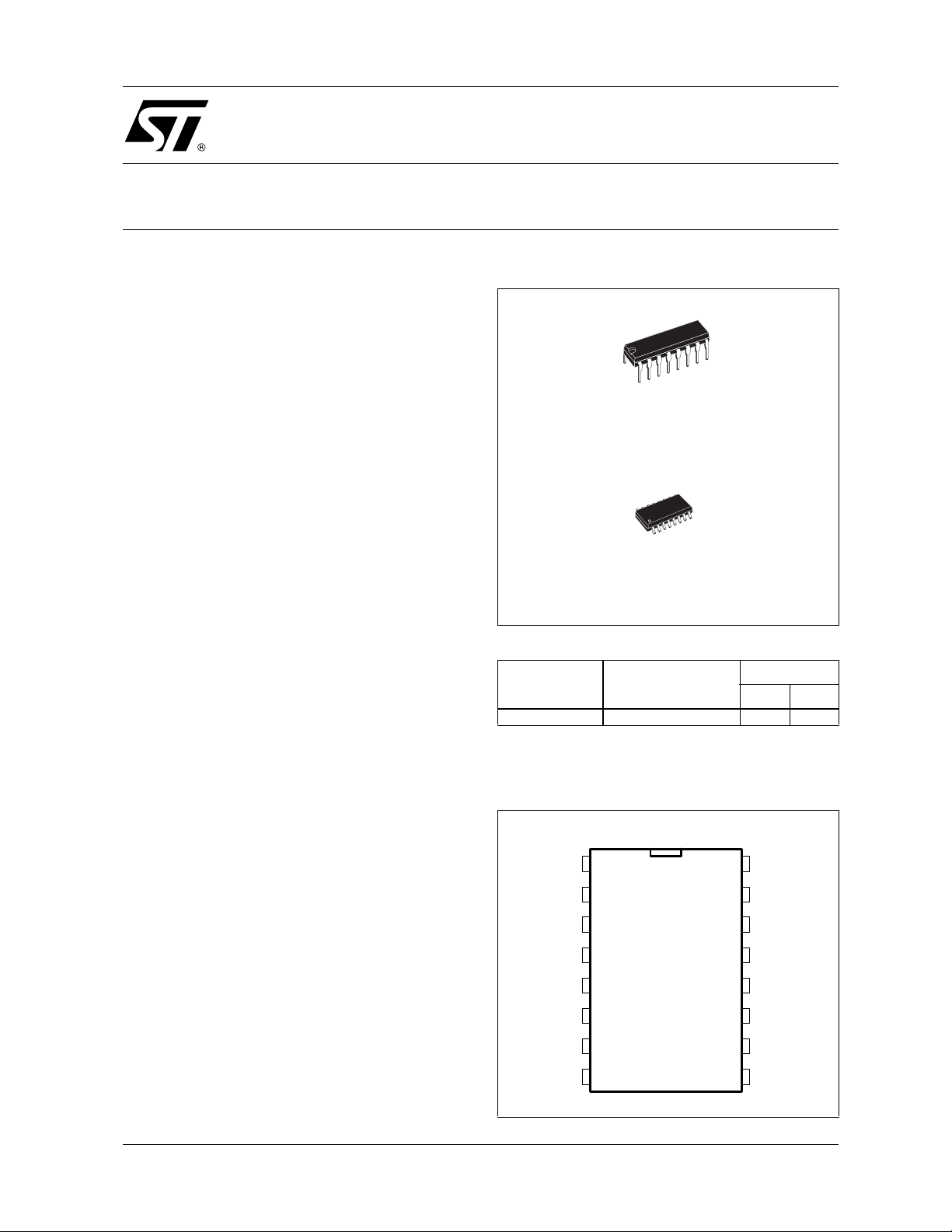
N
DIP-16
(Plastic Package)
D
SO-16
(Plastic Micropacka ge)
ORDER CODE
Part Number Temperature Range
TD310I -40°C, +125°C
N = Dual in Line Package (DIP)
D = Small Outline Package (SO) - also available in Tape & Reel (DT)
Package
ND
••
PIN CONNECTIONS (top view)
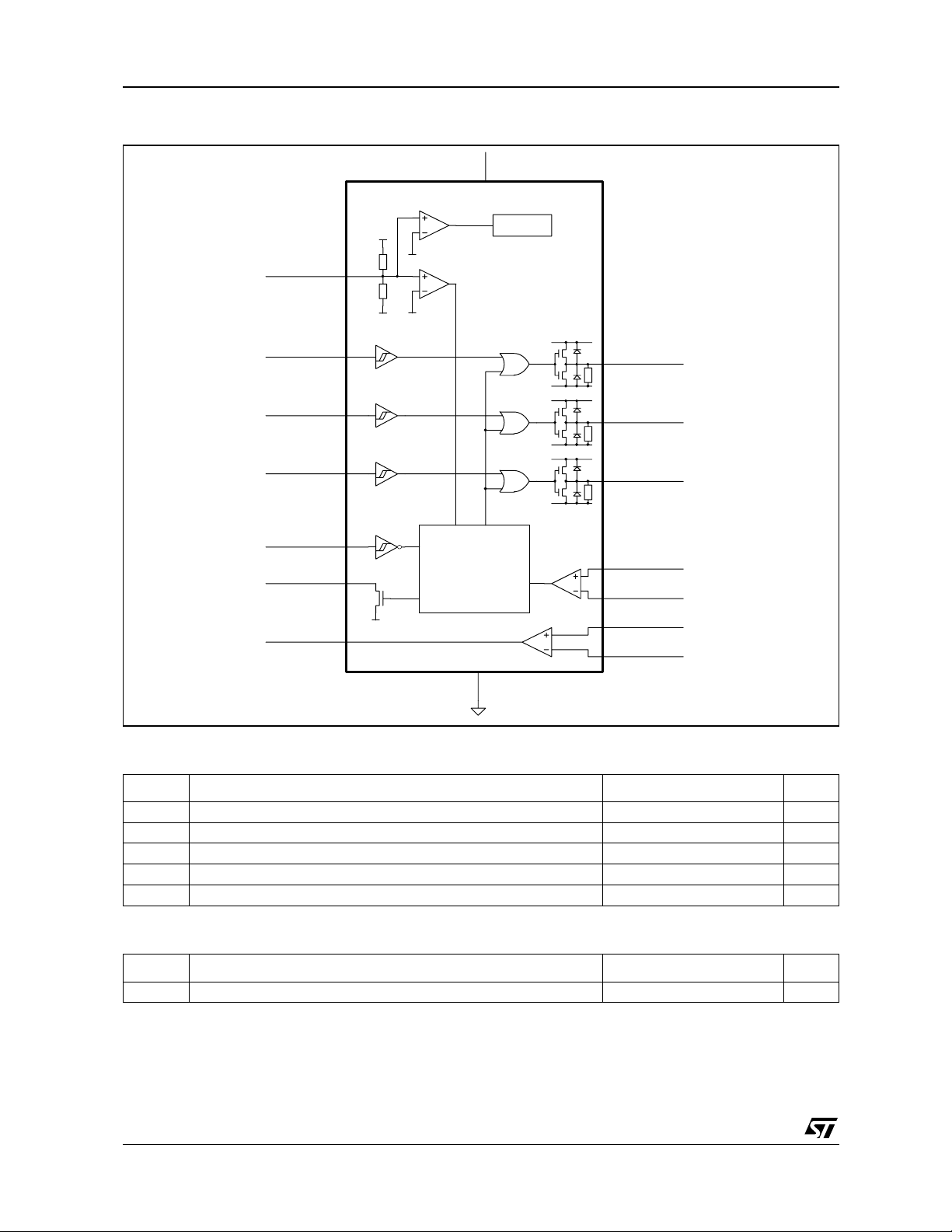
TD310 includes a current sense comparator which
inhibit the output drivers in case of overcurrent. An
alarm output signals the even to a controller.
TD310 also includes an uncommitted op-amp
which can be u sed for current measurement (as
an amplifier before the A/D input of a
microcontroller) of for other general purpose.
Programmable undervo ltage lockout and standby
mode make TD310 suitable for a large area of
environment and application.
Typical applications are low side IG BT and power
MOSFET drive in three phase systems, pulse
transformer drive, and general purpose pulse
drive.
December 2001
VCC
Enable
Alarm
OA Output
OA Input + Sense +
INA
INB
INC
1
2
3
4
5
6
7
16
15
14
13
12
11
10
98
UVLO/Stb
OUTA
OUTB
OUTC
Gnd
Sense OA Input -
1/9
TD310
BLOCK DIAGRAM
VCC
Stby
INA
INB
INC
Enable
Alarm
OA output
1.26M
140k
GND
VCC
GND
0.7V
1.2V
Standby
UVLO
Control
Unit
Standby
TD310
OUTA
OUTB
OUTC
Sense+
Sense -
OA input +
OA Input-
GND
ABSOLUTE MAXIMUM RATINGS
Symbol Parameter Value Unit
V
T
Supply Voltage 18 V
CC
V
Input Voltage
i
V
Sense Input Voltage
is
T
Operating Junction Temperature -40 to 150 °C
j
Operating Ambient Temperature -40 to 125 °C
amb
0 to V
-0.3 to V
CC
CC
V
V
OPERATING CONDITIONS
Symbol Parameter Value Unit
V
Supply Voltage 4 to 16 V
CC
INSTRUCTION FOR USE
1 - The TD310 supply voltage must be decoupled with a 1µF min. capacitor.
2 - If the application involv ing TD310 requires m aximum output current capa bility, this current must be
pulsed: pulse width 1µsec, duty cycle 1% at T
2/9
amb.
TD310
ELECTRICAL CHARACTERISTICS
V
= 15V, T
CC
= 25°C (unless otherwise specified)
amb
Symbol Parameter Min. Typ. Max. Unit
I
Supply Current with Inputs in High State 1.5 2 mA
CC
LOGIC INPUT (all inputs)
V
High Input Voltage 2 V
IH
V
Low Input Voltage 0.8 V
IL
I
High Input Current 10 pA
IH
I
Low Input Current 10 pA
IL
Propagation Delay (10% input to 10% output)
t
dH
tdL, t
t
, t
eL
eH
t
li
dd
Output Delay
Output Delay
≤ Tamb ≤ T
T
min.
max.
Input Inhibiting Time 100 ns
Differential Delay Time Between Channels 20 ns
OUTPUT DRIVERS
V
V
V
R
Sourcing Drop Voltage (A/B/C outputs)
sod
sid
dem
opd
I
= 200mA
source
Sinking Drop Voltage (A/B/C outputs)
Isink = 200mA
Demagnetizing Drop Voltage (A/B/C outputs)
Idemag. = 100mA
Output Pull Down Resistor 47 k
ALARM OUTPUT
Low Level Sinking Current
I
s
I
sh
t
A
V
= 0.8V
O
High Level Sinking Current 1
Alarm Output : Delay Time to Alarm Fall if Sense Input Triggered 500 ns
SENSE INPUT
V
V
Input Offset Voltage 20 mV
ios
t
Inhibition Time if Sense Input Triggered 1 ms
Ai
Delay Time to Output Fall if Sense Input Triggered
t
s
t
si
shys
All outputs inhibited
Inhibition Time of Sense Input 300 ns
Sense Hysteresis 40 mV
OPERATIONAL AMPLIFIER
V
GBP Gain Bandwidth Product 1 MHz
Common Mode Input Voltage Range
icm
V
Input Offset Voltage 10 mV
io
A
Open Loop Gain 60 dB
vd
Slew Rate at Unity Gain (R
SR
= 100kΩ, CL = 100pF, Vi = 3 to 7V)
L
STAND-BY
V
I
Standby Mode Threshold Voltage 0.3 1.1 V
stdby
Standby Mode Supply Current 30
stdby
UNDER VOLTAGE LOCKOUT
I
Under Voltage Level Adjust Current 1
adj
V
V
Internal Stop Threshold (without external adjustment) 10.7 13.3 V
st1
Threshold Hysteresis 0.8 V
hys
200
60
400
400
3V
5V
2V
535 mA
600 ns
CC
+
- 1.5
0 to V
0.6 V/µs
µ
ns
Ω
A
µ
V
A
µ
A/V
3/9

TD310
UVLO/stdby pin functioning modes
Due to the wide supply voltage range o f the TD310, the UVLO function (Under Voltage Lock Out) is
externally adjustable by a resistor bridge.
The bridge rate can be calculated in relation with the expected UVLO protection level as follows :
R1
V
UVLO
The internal resistor sets the default UVLO value to 12V (*) and might influence the external bridge rate if
the values of the external resistors are too high. Moreover, the internal resistor ratio is accurate, but the
the tolerance on the absolute value of each internal resistor (typically 140k and 1.26M) is about +/-20%.
If an external bridge is used, we recommend to choose resistor values not greater than 10k.
The standby threshold value depends of the UVLO value as follows:
-------------------- -
x = 1.2V (where R1 is the lower resistor of the bridge)
R1 R2+
stdby
=
0.7
/
1.2
V
UVLO
+
via a pull up
CC
V
Both UVLO and stdby functions can be inhibited by connec ting the UVLO/stdby pin to V
resistor (ex 150kΩ).
The following table summarizes the functions of the TD310 :
Pin 16 9/11 5 2/3/4 15/14/13 6 7/8/10
Config
Normal 1 H
Stdby 2 L
UVLO 3 M X X X L L OK H
UVLO/
stdby
Sense+/
Sense-
+ > - X X L L
+ < -
+ > + < - H
Enable In A/B/C Out A/B/C Alarm Op-Amp
HIN IN
LX L
XX L
H
L
OK
HZ
Con-
sumption
H
(1.5mA)
L
(30µA)
Configuration 1 : UVLO/stdby = H
The TD310 is in a normal consumption state (1.5mA), the operational amplifier is normally functioning and
the buffer outputs are determined by the sense comparator inputs, the enable inputs and the buffer inputs.
Configuration 2 : UVLO/stdby = L
The TD310 is in a low consumption state (standby mode 30µA), the buffer outputs are set to low state and
the operational amplifier is in high impedance state.
Configuration 3 : UVLO/stdby = M
The VCC supply voltage is between VUVLO and Vstdby (**). The TD310 remains in a normal
consumption state an d the operational amplifier is normally fu nctioning but the buffer outputs and the
alarm pin are set to low state.
(*) If the UVLO level remains unadjusted, it is recommended to bypass the UVLO/stdby pin with a 1nF capacitor.
(**) If the supply voltage falls below V
4/9
, the TD310 is set in standby mode (configuration 2).
stdby

TIMING DIAGRAM
TIMING 1
Input
A/B/C
tdH
Output
A/B/C
TIMING 2
Input
A/B/C
TD310
tli
tdL
Output
A/B/C
Sense
Alarm
Enable
Under
Voltage
ts
tAi
tA
tAi
teL
teH
5/9
TD310
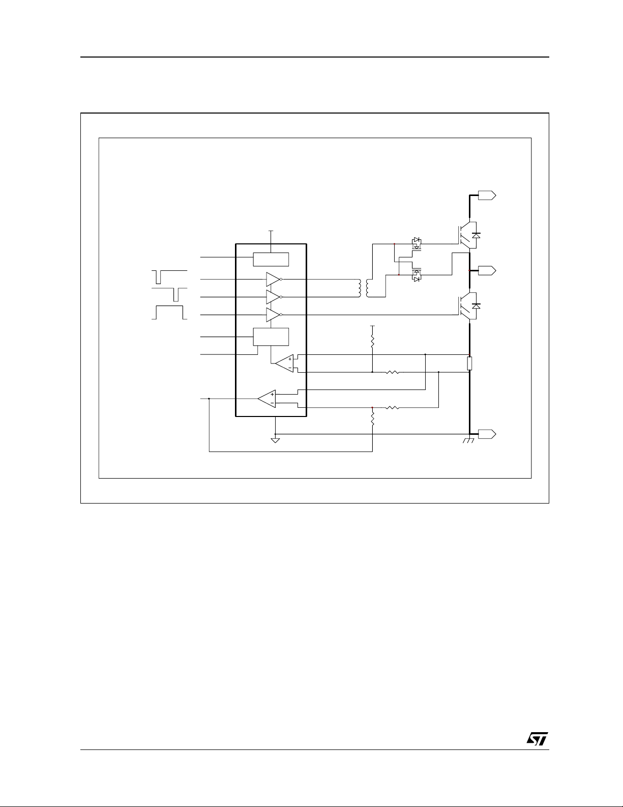
TYPICAL APPLICATIONS
Figure 1 : HALF BRIDGE DRIVE IN THREE PHASE MOTOR SYSTEM
VCC
MCU signals
Pulse controlled inputs
ON
OFF
Level controlled input
Stby
INA
INB
INC
Enable
Alarm
TD310
OA output
VCC
UVLO
Standby
LOGIC
OUTA
OUTB
OUTC
Sense+
Sense -
OA input +
OA Input-
Pulse transf
VCC
High voltage
LOA D
Shunt
GND
GND
6/9
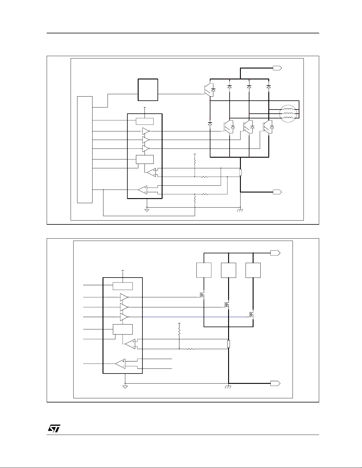
Figure 2 : THREE PHASE MOTOR LOW SIDE DRIVE
TD310
+400V
MICRO
CONTROLLER
HS
STBY
A
B
C
En
IT
ANA
Stby
INA
INB
INC
Enable
Alarm
OA output
Figure 3 : LOW SIDE DRIVE
High Side
Standby
LOGIC
TD310
GND
Driver
VCC
VCC
UVLO
OUTA
OUTB
OUTC
Sense+
Sense -
OA input +
OA Input-
M
VCC
Shunt
GND
Stby
INA
INB
INC
Enable
Alarm
OA output
Standby
LOGIC
TD310
GND
VCC
UVLO
VCC
OUTA
OUTB
OUTC
Sense+
Sense -
OA input +
OA Input-
LOAD LOAD LOAD
VCC
Shunt
GND
7/9

TD310
PACKAGE MECHANICAL DATA
16 PINS - PLASTIC DIP
Dim.
Min. Typ. Max. Min. Typ. Max.
a1 0.51 0.020
B 0.77 1.65 0.030 0.065
b 0.5 0.020
b1 0.25 0.010
D 20 0.787
E 8.5 0.335
e 2.54 0.100
e3 17.78 0.700
F 7.1 0.280
i 5.1 0.201
L 3.3 0.130
Z 1.27 0.050
Millimeters Inches
8/9

PACKAGE MECHANICAL DATA
16 PINS - PLASTIC MICROPACKAGE (SO)
TD310
Dim.
Millimeters Inches
Min. Typ. Max. Min. Typ. Max.
A 1.75 0.069
a1 0.1 0.2 0.004 0.008
a2 1.6 0.063
b 0.35 0.46 0.014 0.018
b1 0.19 0.25 0.007 0.010
C 0.5 0.020
c1 45° (typ.)
D 9.8 10 0.386 0.394
E 5.8 6.2 0.228 0.244
e 1.27 0.050
e3 8.89 0.350
F 3.8 4.0 0.150 0.157
G 4.6 5.3 0.181 0.209
L 0.5 1.27 0.020 0.050
M 0.62 0.024
S 8° (max.)
Information furnished is bel ieved to be accurate and reliable. However, STMicroe lectronics assumes no responsibility for the
consequences of use of such information nor for any infringement of patents or other rights of third parties which may result from
its use. No li cense is granted by i mp lication or otherwise under any patent or pate nt rig hts of STMicroelectronics. S pec ific at ions
mentioned in this publication ar e subject to change without notice. This publication supersedes and replaces all information
previously supplied. S TMicroelectronics products are not authorized for use as critica l components in life suppo rt devices or
systems without express written approval of STMicroelectronics.
© The ST logo is a registered trademark of STMicroelectronics
© 2001 STM icroelectronics - P r inted in Italy - All Righ ts Reserv ed
STMicr o el ectronics GROUP OF COMPA NIES
Australi a - Brazil - Canada - Chin a - F i nl and - Franc e - Germany - Hong Kong - Ind i a - Israel - Ita ly - Japan - Mal aysia
Malta - Mor occo - Singapore - Spain - Sweden - S wi tzerland - United Ki ngdom - Unit ed States
© http://www.st.com
9/9
 Loading...