


P
TD220/221
Gate Driver with VReg and Two Point Regulator
DATASHEET
■ 60mA/120mA MIN GATE DRIVE
■ TWO POINT REGULATOR FOR
SWITCHING CHARGE PUMP SUPPLY
■ 3.3V OR 5V VOLTAGE REGULATOR
■ LOW STARTUP CURRENT
■ UVLO PROTECTIO N
■ 2kV ESD PROTECTION
DESCRIPTION
TD220 is a solution for micro-c ontroller based offline applications. TD220 includes a two point
regulator for power supply generation, a 3.3V
(TD220) or 5V (TD221) linear regulator for the
microcontroller supply, and a MOSFET driver.
APPLICATIONS
■ µC-BASED OFF-LINE APPLICATIONS
ORDER CODE
Part Number
TD220I -25, +125°C
TD221I -25, +125°C
T emperature
Range
Package
D
•
•
Package Reference
D
SO8
(Plastic
MicroPackage )
PIN CONNECTIONS (top view)
VCC
VOUT 7
NC
1
2
3
8
6
VCA
VSUP
GND
Note: D = Small Ou tlin e Pa ckag e ( SO) - al so av aila ble in T ape &
Reel (DT)
May 2003
Revision B 1/8
4
GATEIN
5
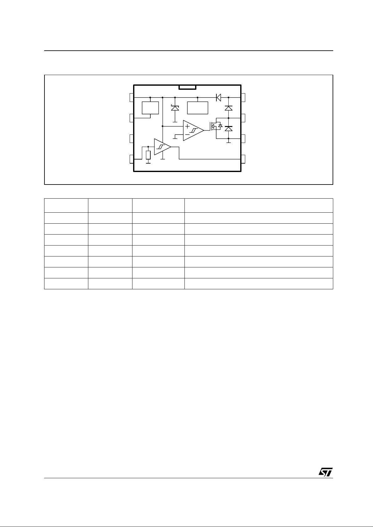
TD220/221 Block Diagram
P
1 BLOCK DIAGRAM
VCC
Vreg UVLO
22V
D1
D2
VOUT
D3
NC
IN
75k
13V
Q1
TPR
Pin Description
Name Pin Number T ype Function
VCC
VOUT
IN
GATE 5
GND 6
VSUP
VCAP
1
2
4
7
8
Power supply Supply capacitor and startup resistor
Analog output +3.3V (TD220) or +5V (TD221) voltage regulator
Digital input Input signal for gate drive
Analog output Gate drive output
Power supply Signal ground
Power supply Charge pump input
Power supply Capacitor for charge pump
VCA
VSUP
GND
GATE
2/8
Absolute Maximum Rating TD220/221
2 ABSOLUTE MAXIMUM RATING
Symbol Parameter Value Unit
VCC
Vout
Vin
Isup
Ipeak
Pd
Tstg
Tj
Rhja
Rhjc
ESD
DC Supply Voltage (Icc<5mA)
Voltage on GATE and VCAP pins
Voltage on IN and VOUT pins
Continuous current in VSUP pin
Peak current in VSUP pin (tp≤1µs, f≤150kHz, see waveform below)
Power dissipation
Storage temperatur e
Maximum Junction Temperature
Thermal Resistance Junction-A mbie nt
Thermal Resistance Junction-C ase
Electrostatic discharge (HBM)
-0.3 to selflimit V
-0.3 to VCC+0.3 V
-0.3 to 7 V
-200 to 200 mA
-1.0 to 1.0 A
500 mW
-55 to 150 °C
150 °C
150 °C/W
40 °C/W
2kV
OPERATING CONDITIONS
Symbol Parameter Value Unit
VCC
Isup
Ipeak
Tj
Supply Voltage
Continuous current in VSUP pin
Peak current in VSUP pin (tp≤1µs, f≤150kHz, see waveform below)
Junction Temperature
UVLO to 17 V
0 to 200 mA
-1.0 to 1.0 A
-25 to 125 °C
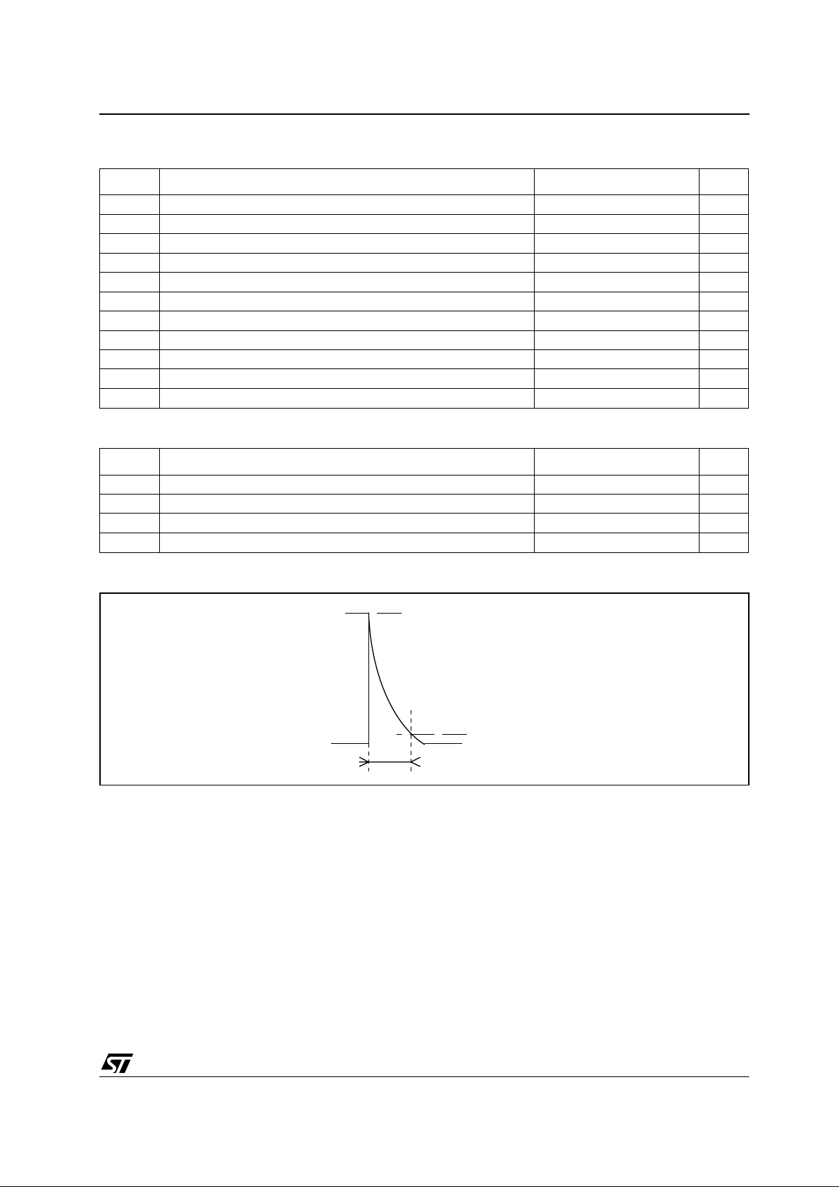
Typical waveform of current in VSUP pin
Ipeak
10mA
tp
3/8

TD220/221 Electrical Characteristics
3 ELECTRICAL CHARACTERISTICS
Tamb = 25°C, VCC=13V unless otherwise specified
Symbol Parameter Test Condition Min Typ Max Unit
Supply
Icc
Icc2
Istby
Vclamp
Inpu t
Vton
Vtoff
Vh
Iinpl
Iinph
Voltage regulator
Vout
RegLoad
Ipeak
dVout
Cout
Ileak
Vrip
Vnoise
tstartup
tsettle
T wo Point Regulator (TPR)
VTPROn
VTPR Of f
VTPRH
VF
Supply current no load at any pin, Vin<1V
Tamb=25°C
-25°C<Tj<125°C
1nF GATE load,
300kHz IN signal
Standby current UVLO active
Tamb=25°C
-25°C<Tj<125°C
Clamp voltage Icc<5mA
IN Turn-on Threshold Voltage
IN Turn-off Threshold Voltage
IN Hysteresis
IN Input current low Vin<0.5V
IN Input current high Vin=3.3V
Voltage reference Iout=10mA
TD220
TD221
Load Regulation Iout change from 10mA
to 25mA
Peak output current Vout=1V
Temperature coefficent Iout=10mA
Allowed capacitive load - Note 1 Iout=10mA
Leakage current in UVLO state Vout=1V
Ripple rejection - Note 1 f=100Hz
f=10kHz
Noise voltage 100Hz<f<100kHz
Startup time (Vout>3.1V) Cout=1µF
Settling time (1% final value) Cout=1µF
Turn-on level
Turn-off level
Hysteresis =VTPROn-VTPROff
Forward voltage D1 IF=200mA
0.7 1.0
456mA
160
20 22 24 V
1.8 2.1 V
1.0 1.3 V
0.5 V
3.20
4.85
100 mA
0.1 1
40
20
12.4 V
0.23 0.29 0.35 V
3.30
5
1mV
2ms
1.2
230
20
100
3.40
5.15
50 mV
250 ppm/°C
10
0.1 ms
13.6 V
1.5 V
mA
mA
µ
µ
µ
µ
V
V
µ
µ
dB
dB
A
A
A
A
F
A
4/8

Electrical Characteristics TD220/221
Symbol Parameter Test Condition Min Typ Max Unit
Gate Output
VOL
VOH
Isink
Isrc
VOL2
tgmin
tpd
Output low voltage Igate=10mA
Output high voltage Igate=-10mA
Output sink current Vgate=6V
Output source current Vgate=3V
Output low voltage in UVLO state Vcc=6V, Igate=1mA
Minimum output pulse width
IN to GATE propagation delay
Under Voltage Lockout (UVLO)
UVLOH
UVLOL
Vhyst
1) Not 100% tested. Guaranteed by design.
UVLO top threshold
UVLO bottom threshold
UVLO Hysteresis Vhyst=UVLO H-UV LOL
VCC-2.0 V
Tj=25°C
-25°C < Tj < 125°C 120
Tj=25°C
-25°C < Tj < 125°C 60
1
Cgate=10pF
7.8 8.7 V
5V
300 mA
150 mA
200 ns
0.5 V
mA
mA
2V
80 ns
15 V
5/8

TD220/221 Timing Diagrams
u
4 TIMING DIAGRAMS
Fig. 1: Power up and power down
UVH
UVL
VCC
Icc
GATE
VOUT
Istby
VOL2
1V
Tstartup
Vccmin
Fig. 2: Two point regulator
VCC
VSUP
APPLICATION DIAGRAM
HV DC in
R?
VCC
C?
1uF
VOUT
C?
220nF
13.6V
12.4V
Vreg UVLO
13V
22V
TPR
300mV
VCAP
GND
D?
L?
C?
Q?
R?
VCAP
D1
D2
VSUP
D3
Q1
GND
C?
10uF
HV DC o
C?
DC supply
6/8
µC
IN
GATE

Typical Performance Curves TD220/221
5 TY PICAL PERFORMANCE CURVES
Fig. 3: Supply Current vs Temperature
1.2
1.0
0.8
0.6
Icc (mA)
0.4
0.2
0.0
-25 0 25 50 75 10 0 125
Temp (°C)
Fig. 4: Gate Drive Sink Current vs Temperature
500
400
Fig. 6: Standby Current vs Temperature
250
200
150
100
Istby (µA)
50
0
-25 0 25 50 75 100 125
Temp (°C)
Fig. 7: Gate Drive Source Current vs Temp.
250
225
200
300
Isink (mA)
200
100
-25 0 25 50 75 100 125
Temp (°C )
Fig. 5: Vreg Output Voltage vs T emperature
1.03
1.03
1.02
1.02
1.01
1.01
1.00
1.00
0.99
0.99
normalized Vout
normalized Vout
0.98
0.98
0.97
0.97
-25 0 25 50 75 100 125
-25 0 25 50 75 100 125
Temp (°C)
Temp (°C)
Iout=10mA
Iout=10mA
175
Isrc (mA)
150
125
100
-25 0 25 50 75 100 125
Temp (°C)
7/8

TD220/221 Package Mechanical Data
6 PACKAGE MECHANICAL DATA
SO-8 MECHANICAL DATA
DIM.
A 1.35 1.75 0.053 0.069
A1 0.10 0.25 0.04 0.010
A2 1.10 1.65 0.043 0.065
B 0.33 0.51 0.013 0.020
C 0.19 0.25 0.007 0.010
D 4.80 5.00 0.189 0.197
E 3.80 4.00 0.150 0.157
e 1.27 0.050
H 5.80 6.20 0.228 0.244
h 0.25 0.50 0.010 0.020
L 0.40 1.27 0.016 0.050
k ˚ (max.)
ddd 0.1 0.04
MIN. TYP MAX. MIN. TYP. MAX.
mm. inch
8
0016023/C
Information furnished is bel ieved to be accurate and reliable. However, STMicroelec tronics assumes no responsibility for the
consequences of use of such information nor for any infringement of patents or other rights of third parties which may result from
its use. No li cense is granted by implicat i on or otherwise under a ny patent or patent righ ts of STMicroelectronics. Specific ations
mentioned in this publica tion are subject to change without notice. Thi s publication supersedes and replaces all information
previously supplied. STMicroelectronics products are not authorized for use as critical components in life support devices or
systems without express written approval of STMicroelectronics.
Australi a - Brazil - Chi na - Finland - F rance - Germany - Hong Kon g - In dia - Italy - Japan - Malaysi a - M alta - Moroc co
The ST logo is a registered trademark of STMicroelectronics
© 2003 STMicroelectronics - All Rights Reserved
STMicroelectroni cs GROUP OF COMPANIES
Singapo re - Spain - Sweden - Switzerland - Un i ted Kingdom
http://www.st.com
8/8
 Loading...