

®
TBA820M
1.2W AUDIO AMPLIFIER
DESCRIPTION
The TBA820M is a monolithic integrated audio
amplifier in a 8 lead dual in-line plastic package. It
is intended for use as low frequency class B po wer
amplifier with wide range of supply voltage: 3 to
16V, in portable radios, cassette recorders and
players etc. Main features are: minimum working
supply voltage of 3V, low quiescent current, low
number of external components, good ripple rejection, no cross-over distortion, low power dissipation.
Output power: P
= 2W at 12V/8Ω, 1.6W at 9V/4
o
Ω
ORDERING NUMBER: TBA820M
and 1.2W at 9V/8Ω.
ABSOLUTE MAXIMUM RATINGS
Symbol Parameter Value Unit
Supply voltage 16 V
V
s
I
Output peak current 1.5 A
o
P
T
stg
Pow er dissipatio n at T
tot
, TjStorage and junction temperature -40 to 150
amb
= 50°C
Minidip
1W
C
°
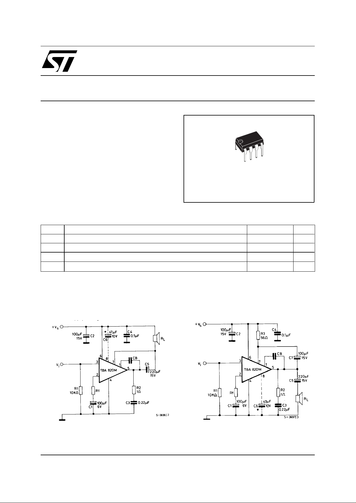
TEST AND APPLICATION CIRCUITS
Figure 1. Ci rcuit diagram with load con nected to the
supply voltage
September 2003
Figure 2. Cir cuit diagram w ith load connected
to ground
* Capacitor C6 must be used when high ripple
rejection is requested.
1/6
TBA820M
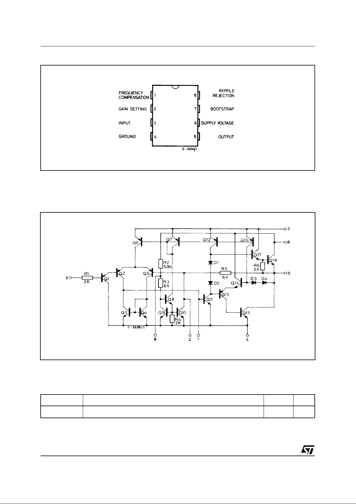
PIN CONNECTION
(top view)
SCHEMATIC DIAGRAM
THERMAL DATA
Symbol Parameter Value Unit
2/6
R
th-j-amb
Thermal resistance junction-ambient max 100
C/W
°

TBA820M
ELECTRICAL CHARACTERISTICS
(Refer to the test circuits Vs = 9V, T
= 25 °C unless otherwise
amb
specified)
Symbol Parameter Test conditions Min. Typ. Max. Unit
V
Supply voltage 3 16 V
s
V
P
C
Quiescent output voltage (pin 5) 4 4.5 5 V
o
Quiescent drain current 4 12 mA
I
d
I
Bias current (pin 3) 0.1
b
o
Output power
d = 10%
R
= 120
f
V
= 12V
s
V
= 9V
s
= 9V
V
s
V
= 6V
s
= 3.5V
V
s
Ω
f = 1 kHz
R
= 8
Ω
L
R
= 4
Ω
L
R
= 8
Ω
L
R
= 4
Ω
L
R
= 4
Ω
L
0.9
2
1.6
1.2
0.75
0.25
Ri Input resistance (pin 3) f = 1 kHz 5
B Frequency response (-3 dB)
d Distortion
R
= 8
Ω
L
C
= 1000 µF
5
= 120
R
f
P
= 500 mW
o
= 8
R
Ω
L
f = 1 kHz
Ω
C
= 680 pF 25 to 7,000
B
= 220 pF 25 to 20,000
B
R
= 33
Ω
f
R
= 120
Ω
f
0.8
0.4
µ
M
Hz
A
W
W
W
W
W
Ω
%
G
G
Voltage gain (open loop) f = 1 kHz
v
Voltage gain (closed loop)
v
= 8
R
L
f = 1 kHz
e
S + N
SVR Supply voltage rejection
Input noise voltage (*) 3
N
Input noise current (*) 0.4 nA
i
N
P
Signal to noise ratio (*)
N
(test circuit of fig. 2)
= 1.2W
o
= 8
R
L
G
= 34 dB
v
R
= 8
L
f
(ripple)
C6 = 47 µF
= 120
R
f
(*) B = 22 Hz to 22 KHz
Ω
Ω
Ω
= 100 Hz
Ω
= 8
R
Ω
L
Rf = 33
Ω
R
= 120
f
R1 = 10K
R1 = 50 k
75 dB
45
Ω
Ω
34
80
dB
µ
V
dB
Ω
70
42 dB
3/6

TBA820M
Figure 3. Output power vs.
supply voltage
Figure 6. Maximum power
dissipation (sine wave
operation)
Figure 4. Harmonic distortion
vs. output power
Figure 7. Suggested value of
vs. R
C
B
f
Figure 5. Power dissipation
and efficiency vs. output
power
Figure 8. Frequency response
Figure 9. Harmonic dis tortion
vs. frequency
4/6
Figure 10. Supply voltage
rejection (Fig. 2 circuit)
Figure 11. Quiescent current
vs. supply voltage

mm inch
DIM.
MIN. TYP. MAX. MIN. TYP. MAX.
A 3.32 0.131
a1 0.51 0.020
B 1.15 1.65 0.045 0.065
b 0.356 0.55 0.014 0.022
b1 0.204 0.304 0.008 0.012
D 10.92 0.430
E 7.95 9.75 0.313 0.384
e2.54 0.100
e3 7.62 0.300
e4 7.62 0.300
F 6.6 0.260
TBA820M
OUTLINE AND
MECHANICAL DATA
I 5.08 0.200
L 3.18 3.81 0.125 0.150
Z 1.52 0.060
Minidip
5/6

TBA820M
Information furnished is believed to be accurate and reliable. Howev er, STMicroelectronics assumes no responsibility for the consequen ces of
use of such information nor for any infringement of patents or other ri ght s of third parties which may result from its use. No license is granted
by implication or otherwise under any patent or patent rights of STMicroelectronics. Specifications mentioned in this publication are subject to
change without not ice. This publication supersedes and repl aces all information pr eviously supplied. STMicroelectronics pr oducts are not
authorized for use as critical components in life support devices or systems without express written approval of STMicroelectronics.
The ST logo is a registered trademark of STMicroelectronics.
All other names are the property of their respective owners
© 2003 STMicroelectronics - All rights reserved
STMicroelectronics GROUP OF COMPANIES
Australia – Belgium - Brazil - Canada - China – Czech Republic - Finland - France - Germany - Hong Kong - India - Israel - Italy - Japan -
Malaysia - Malta - Morocco - Singapore - Spain - Sweden - Switzerla nd - United Kingdom - United States
www.st.com
6/6
 Loading...