


T8T
Snubberless™, logic level and standard 8 A Triacs
Features
■ Medium current Triac
■ High static and dynamic commutation
■ Low thermal resistance with clip bonding
■ Packages is RoHS (2002/95/EC) compliant
■ 600 V V
■
UL certified (ref. file E81734)
RM
Applications
■ Value sensitive application
■ General purpose ac line load switching
■ Motor control circuits in power tools
■ Small home appliances, lighting
■ Inrush current limiting circuits
■ Overvoltage crowbar protection
Description
Available in through-hole, the T8T series of Triacs
can be used as on/off or phase angle control
function in general purpose ac switching where
high commutation capability is required.
A2
G
A1
A1
A2
G
TO-220AB insulated
(T8xxT-6I)
Table 1. Device summary
Order code Symbol Value
3Q
I
T810T-6I
T820T-6I
T835T-6I
T825T-6I
GT
logic level
3Q
I
GT
Snubberless
4Q
I
GT
standard
20 / 35 mA
10 mA
25 mA
This series can be designed-in in many value
sensitive appliances thanks to the parameters
guidance provided in the following pages.
Provides insulation rated at 2500 V rms
(TO-220AB insulated package).
TM: Snubberless is a trademark of STMicroelectronics
September 2011 Doc ID 16192 Rev 3 1/9
www.st.com
9

Characteristics T8T
1 Characteristics
Table 2. Absolute ratings (limiting values; Tj = 25 °C, unless otherwise specified)
Symbol Parameter Value Unit
I
T(RMS)
I
dI/dt
V
DSM
V
I
P
G(AV)
T
On-state rms current (full sine wave) Tc = 97 °C 8 A
Non repetitive surge peak on-state current
TSM
(full cycle, Tj initial = 25 °C)
²
tI²t Value for fusing tp = 10 ms 26 A²s
I
Critical rate of rise of on-state current I
= 2 x IGT
G
tr ≤ 100 ns
/
Non repetitive surge peak off-state
voltage
RSM
Peak gate current tp = 20 µs Tj = 125 °C 4 A
GM
F = 50 Hz t
F = 60 Hz t
F = 60 Hz T
= 10 ms Tj = 25 °C
t
p
= 20 ms 60
p
= 16.7 ms 63
p
= 125 °C 50 A/µs
j
V
DRM/VRRM
+ 100
Average gate power dissipation Tj = 125 °C 1 W
Storage junction temperature range - 40 to + 150 °C
stg
Operating junction temperature range - 40 to + 125 °C
T
j
A
V
2/9 Doc ID 16192 Rev 3

T8T Characteristics
Table 3. Electrical characteristics (Tj = 25 °C, unless otherwise specified)
T8xxT
Symbol Test conditions Quadrant
T810T T820T T825T T835T
I
GT
V
V
I
H
(1)
VD = 12 V, RL = 30 Ω
I - II - III
MAX.
IV 40
VD = V
GT
Tj = 25 °C
VD = V
GD
(2)
= 125 °C
T
j
IT = 500 mA MAX. 15 25 30 40 mA
, RL = 30 Ω,
DRM
, RL = 3.3 kΩ,
DRM
ALL MAX. 1.3 V
ALL MIN. 0.2 V
I - III
IG = 1.2 I
I
L
GT
MAX.
10 20 25 35
20 35 40 50
II 25 40 70 70
dV/dt
(di/dt)c
(2)
VD = 67% V
DRM,
gate open
Tj = 125 °C
= 150 °C
T
j
(3)
MIN.
(dV/dt)c = 0.1 V/µs
(dV/dt)c = 10 V/µs 2 4.5
Without snubber 3.4 8
(2)
(dV/dt)c = 0.1 V/µs
(dV/dt)c = 10 V/µs 1 2
Tj = 125 °C
= 150 °C
T
j
MIN.
(3)
100 750 500 2000
50 500 300 1000
5.4
2.5
Without snubber 2 6.5
1. Minimum IGT is guaranted at 5% of IGT max.
2. For both polarities of A2 referenced to A1.
3. Derating information for excess temperature above T
Table 4. Static characteristics
max.
j
Unit
mA
mAIV 40
V/µs
A/ms
Symbol Test conditions Value Unit
(1)
V
ITM = 11.3 A, tp = 380 µs Tj = 25 °C MAX. 1.60 V
T
(1)
V
TO
R
D
I
DRM
I
RRM
1. For both polarities of A2 referenced to A1.
2. Derating information for excess temperature above T
Threshold voltage Tj = 125 °C MAX. 0.87 V
(1)
Dynamic resistance Tj = 125 °C MAX. 60 mΩ
Tj = 25 °C
V
DRM
V
= 0.9 x V
D
= V
RRM
DRM
max.
j
= 125 °C 1
T
j
Tj = 150 °C
(2)
MAX.
TYP. 1.9
5µA
Doc ID 16192 Rev 3 3/9
mA
Characteristics T8T
Table 5. Thermal resistance
Symbol Parameter Value Unit
R
R
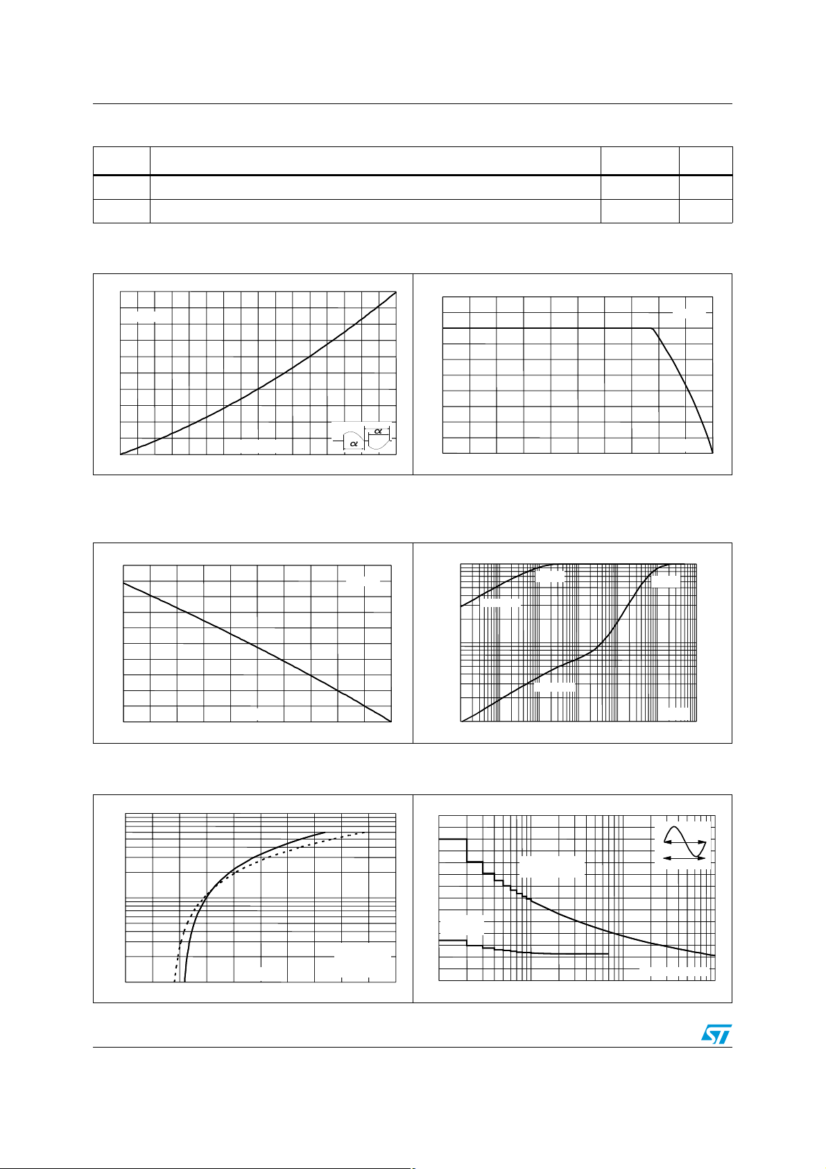
Figure 1. Maximum power dissipation versus
10
10
9
9
8
8
7
7
6
6
5
5
4
4
3
3
2
2
1
1
0
0
Figure 3. On-state rms current versus
Junction to case (AC) 2.8 °C/W
th(j-c)
Junction to ambient (DC) 60 °C/W
th(j-a)
Figure 2. On-state rms current versus case
rms on-state current
P(W)
α = 180°
180°
I
(A)
T(RMS)
012345678
012345678
I
T(RMS)
10
10
9
9
8
8
7
7
6
6
5
5
4
4
3
3
2
2
1
1
0
0
0 25 50 75 100 125
0 25 50 75 100 125
temperature
(A)
Figure 4. Relative variation of thermal
ambient temperature
impedance versus pulse duration
α = 180°
TC(°C)
(free air convection)
I
2.5
2.5
2.0
2.0
T(RMS)
(A)
α = 180°
1.0E+00
K = [Zth/ Rth]
TO-220AB
Z
th(j-c)
Z
th(j-a)
1.5
1.5
1.0E-01
1.0
1.0
0.5
0.5
0.0
0.0
0 25 50 75 100 125
0 25 50 75 100 125
Ta(°C)
Figure 5. On-state characteristics
1.0E-02
Figure 6. Surge peak on state current versus
(maximum values)
ITM(A)
100
100
10
10
Tjmax:
Vto= 0.87 V
1
1
02345
02345
1
VTM(V)
Rd=6 0 mΩ
70
70
60
60
50
50
40
40
30
30
20
20
10
10
0
0
TO-220AB
Tp(s)
1.0E-03 1.0E-02 1.0E-01 1.0E+00 1.0E+01 1.0E+02 1.0E+03
number of cycles
I
(A)
TSM
Non repetitive
Tjinitial = 25 °C
Repetitive
Tc= 97 °C
1 10 100
1 10 100
t = 20 ms
One cycle
Number of cycles
1000
4/9 Doc ID 16192 Rev 3

T8T Characteristics
Figure 7. Non repetitive surge peak on-state
current for a sinusoidal
I
(A), I²t (A²s)
TSM
1000
1000
dl /dt limitation: 50 A / µs
100
100
Tjinitial = 25 °C
I
TSM
I²t
pulse with width t <10 ms, and corresponding value of I²t
10
10
0.01 0.10 1.00 10.00
0.01 0.10 1.00 10.00
p
tp(ms)
Figure 9. Relative variation of holding
current and latching current versus
junction temperature
IH,[Tj] / IH,IL[Tj= 25 °C]I
L
2.0
2.0
1.5
1.5
1.0
1.0
0.5
0.5
0.0
0.0
-50 -25 0 25 50 75 100 125
-50 -25 0 25 50 75 100 125
Tj(°C)
typical values
I
H
I
L
Figure 11. Relative variation of critical rate of
decrease of main current versus
junction temperature
(dl / dt)c[Tj] / [Tj= 125 °C](dl / dt)
6
5
4
3
2
1
0
25 50 75 100 125
c
Tj(°C)
Figure 8. Relative variation of gate trigger
current and gate trigger voltage
versus junction temperature
IGT,VGT[Tj] / IGT,VGT[Tj= 25 °C]
3.0
3.0
2.5
2.5
2.0
2.0
1.5
1.5
1.0
1.0
0.5
0.5
0.0
0.0
-50 -25 0 25 50 75 100 125
-50 -25 0 25 50 75 100 125
IGTQ3
IGTQ1-Q2
IGTQ1-Q2-Q3
Tj(°C)
typical values
Figure 10. Relative variation of static dV/dt
immunity versus junction
temperature
dV / dt [Tj] / [Tj= 125 °C]dV / dt
7
6
5
4
3
2
1
0
25 50 75 100 125
VD=VR= 402 V
Tj(°C)
Figure 12. Relative variation of leakage
current versus junction
temperature
I
DRM/IRRM[Tj;VDRM/VRRM
1.0E+00
1.0E-01
1.0E-02
1.0E-03
25 50 75 100 125
[Tj= 125 °C; 600 V]
V
DRM=VRRM
] / I
DRM/IRRM
V
DRM=VRRM
= 400 V
for different values of blocking voltage
= 600 V
V
DRM=VRRM
= 200 V
Tj(°C)
Doc ID 16192 Rev 3 5/9

Ordering information scheme T8T
2 Ordering information scheme
Figure 13. Ordering information scheme
T 8 10 T - 6 I
TRIAC
Current
8 = 8 A
Sensitivity
10 = 10 mA
20 = 20 mA
25 = 25 mA
35 = 35 mA
Application specific
Voltage
6 = 600 V
Package
I = TO-220AB-Ins.
6/9 Doc ID 16192 Rev 3

T8T Package mechanical data
3 Package mechanical data
● Epoxy meets UL94, V0
● Lead-free packages
In order to meet environmental requirements, ST offers these devices in different grades of
ECOPACK
specifications, grade definitions and product status are available at: www.st.com
ECOPACK
Table 6. TO-220AB Insulated dimensions
®
packages, depending on their level of environmental compliance. ECOPACK®
®
is an ST trademark.
.
Dimensions
Ref.
Millimeters Inches
Min. Typ. Max. Min. Typ. Max.
A 15.20 15.90 0.598 0.625
a1 3.75 0.147
B
Ø I
L
A
I4
l3
a1
l2
a2
C
b2
a2 13.00 14.00 0.511 0.551
B 10.00 10.40 0.393 0.409
F
b1 0.61 0.88 0.024 0.034
b2 1.23 1.32 0.048 0.051
C 4.40 4.60 0.173 0.181
c2
c1 0.49 0.70 0.019 0.027
c2 2.40 2.72 0.094 0.107
e 2.40 2.70 0.094 0.106
b1
e
M
F 6.20 6.60 0.244 0.259
c1
ØI 3.75 3.85 0.147 0.151
I4 15.80 16.40 16.80 0.622 0.646 0.661
L 2.65 2.95 0.104 0.116
l2 1.14 1.70 0.044 0.066
l3 1.14 1.70 0.044 0.066
M2.60 0.102
Doc ID 16192 Rev 3 7/9

Ordering information T8T
4 Ordering information
Table 7. Ordering information
Order code Marking Package Weight Base qty Delivery mode
T810T-6I T810T-6I
T820T-6I T820T-6I
T825T-6I T825T-6I
T835T-6I T835T-6I
5 Revision history
Table 8. Document revision history
Date Revision Changes
10-Sep-2009 1 First issue.
18-Jan-2010 2 Updated pag.1.
20-Sep-2011 3 Updated: Features.
TO-220AB-Ins. 2.3 g 50 Tube
8/9 Doc ID 16192 Rev 3

T8T
Please Read Carefully:
Information in this document is provided solely in connection with ST products. STMicroelectronics NV and its subsidiaries (“ST”) reserve the
right to make changes, corrections, modifications or improvements, to this document, and the products and services described herein at any
time, without notice.
All ST products are sold pursuant to ST’s terms and conditions of sale.
Purchasers are solely responsible for the choice, selection and use of the ST products and services described herein, and ST assumes no
liability whatsoever relating to the choice, selection or use of the ST products and services described herein.
No license, express or implied, by estoppel or otherwise, to any intellectual property rights is granted under this document. If any part of this
document refers to any third party products or services it shall not be deemed a license grant by ST for the use of such third party products
or services, or any intellectual property contained therein or considered as a warranty covering the use in any manner whatsoever of such
third party products or services or any intellectual property contained therein.
UNLESS OTHERWISE SET FORTH IN ST’S TERMS AND CONDITIONS OF SALE ST DISCLAIMS ANY EXPRESS OR IMPLIED
WARRANTY WITH RESPECT TO THE USE AND/OR SALE OF ST PRODUCTS INCLUDING WITHOUT LIMITATION IMPLIED
WARRANTIES OF MERCHANTABILITY, FITNESS FOR A PARTICULAR PURPOSE (AND THEIR EQUIVALENTS UNDER THE LAWS
OF ANY JURISDICTION), OR INFRINGEMENT OF ANY PATENT, COPYRIGHT OR OTHER INTELLECTUAL PROPERTY RIGHT.
UNLESS EXPRESSLY APPROVED IN WRITING BY TWO AUTHORIZED ST REPRESENTATIVES, ST PRODUCTS ARE NOT
RECOMMENDED, AUTHORIZED OR WARRANTED FOR USE IN MILITARY, AIR CRAFT, SPACE, LIFE SAVING, OR LIFE SUSTAINING
APPLICATIONS, NOR IN PRODUCTS OR SYSTEMS WHERE FAILURE OR MALFUNCTION MAY RESULT IN PERSONAL INJURY,
DEATH, OR SEVERE PROPERTY OR ENVIRONMENTAL DAMAGE. ST PRODUCTS WHICH ARE NOT SPECIFIED AS "AUTOMOTIVE
GRADE" MAY ONLY BE USED IN AUTOMOTIVE APPLICATIONS AT USER’S OWN RISK.
Resale of ST products with provisions different from the statements and/or technical features set forth in this document shall immediately void
any warranty granted by ST for the ST product or service described herein and shall not create or extend in any manner whatsoever, any
liability of ST.
ST and the ST logo are trademarks or registered trademarks of ST in various countries.
Information in this document supersedes and replaces all information previously supplied.
The ST logo is a registered trademark of STMicroelectronics. All other names are the property of their respective owners.
© 2011 STMicroelectronics - All rights reserved
STMicroelectronics group of companies
Australia - Belgium - Brazil - Canada - China - Czech Republic - Finland - France - Germany - Hong Kong - India - Israel - Italy - Japan -
Malaysia - Malta - Morocco - Philippines - Singapore - Spain - Sweden - Switzerland - United Kingdom - United States of America
www.st.com
Doc ID 16192 Rev 3 9/9
 Loading...