

Features
■ Medium current TRIAC
■ Logic level sensitive TRIAC
■ 150 °C max. T
■ Clip bounding
■ RoHS (2002/95/EC) compliant package
turn-off commutation
j
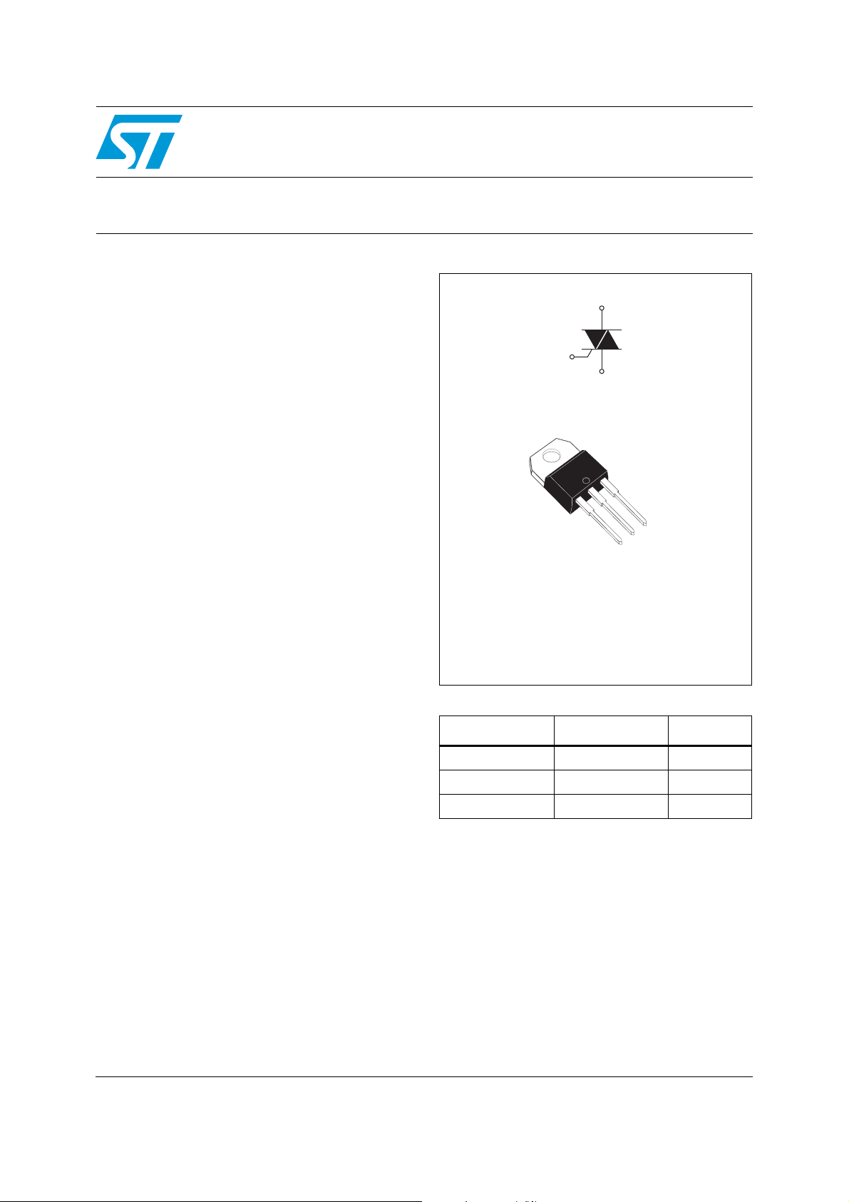
T410H
High temperature 4 A sensitive TRIACs
A2
G
A1
Applications
■ The T410H is designed for the control of AC
actuators in appliances and industrial systems.
■ The multi-port drive of the microcontroller can
control the multiple loads of such appliances
and systems through this sensitive gate
TRIAC.
Description
Specifically designed to operate at 150 °C, the
new 4 A T410H TRIAC provides an enhanced
performance in terms of power loss and thermal
dissipation. This allows the optimization of the
heatsink size, leading to space and cost
effectiveness when compared to electromechanical solutions.
Based on ST logic level technology, the T410H
offers an I
minimal commutation and high noise immunity
levels valid up to the T
lower than 10 mA and specified
GT
max.
j
A2
A2
A1
TO-220AB
T410H-6T
Table 1. Device summary
Symbol Value Unit
I
T(RMS)
V
DRM/VRRM
I
GT MAX
4A
600 V
10 mA
G
May 2009 Doc ID 15712 Rev 1 1/9
www.st.com
9
Characteristics T410H
1 Characteristics
Table 2. Absolute maximum ratings
Symbol Parameter Value Unit
I
T(RMS)
I
TSM
²
tI
I
dI/dt
V
DSM/VRSM
I
GM
P
G(AV)
T
stg
T
j
Table 3. Electrical characteristics (Tj = 25 °C, unless otherwise specified)
On-state rms current (full sine wave) Tc = 141 °C 4 A
Non repetitive surge peak on-state current
(full cycle, Tj initial = 25 °C)
²
t Value for fusing tp = 10 ms 11 A²s
Critical rate of rise of on-state current
I
= 2 x IGT , tr ≤ 100 ns
G
Non repetitive surge peak off-state voltage tp = 10 ms Tj = 25 °C
F = 60 Hz t = 16.7 ms 42
F = 50 Hz t = 20 ms 40
F = 120 Hz T
= 150 °C 50 A/µs
j
V
DRM/VRRM
+ 100
Peak gate current tp = 20 µs Tj = 150 °C 4 A
Average gate power dissipation Tj = 150 °C 1 W
Storage junction temperature range
Operating junction temperature range
- 40 to + 150
- 40 to + 150
Symbol Test conditions Quadrant Min. Max. Unit
I
GT
V
GT
V
GD
(1)
I
H
VD = 12 V RL = 33 Ω
VD = V
, RL = 3.3 kΩ I - II - III 0.15 V
DRM
IT = 100 mA 25 mA
I - II - III 1 10 mA
I - II - III 1.0 V
I - III 30
I
L
dV/dt
(dI/dt)c
1. For both polarities of A2 referenced to A1.
IG = 1.2 I
(1)
VD = 67% V
Logic level, 0.1 V/µs, Tj = 150 °C 5.7
(1)
Logic level, 15 V/µs, T
GT
II 35
gate open, Tj = 150 °C 75 V/µs
DRM,
= 150 °C 1.5
j
A
V
°C
mA
A/ms
2/9 Doc ID 15712 Rev 1
T410H Characteristics
(A)
Table 4. Static characteristics
Symbol Test conditions Value Unit
(1)
V
T
V
t0
(1)
R
d
ITM = 5.6 A, tp = 380 µs Tj = 25 °C MAX. 1.5 V
(1)
Threshold voltage Tj = 150 °C MAX. 0.80 V
Dynamic resistance Tj = 150 °C MAX. 80.0 mΩ
Tj = 25 °C MAX. 5 µA
V
= V
I
DRM
I
RRM
V
DRM
D/VR
D/VR
RRM
= 150 °C MAX. 2.2
T
j
= 400 V (at peak mains voltage) Tj = 150 °C MAX. 1.75
= 200 V (at peak mains voltage) Tj = 150 °C MAX. 1.5
1. for both polarities of A2 referenced to A1.
Table 5. Thermal resistance
Symbol Parameter Value Unit
R
th(j-c)
R
th(j-a)
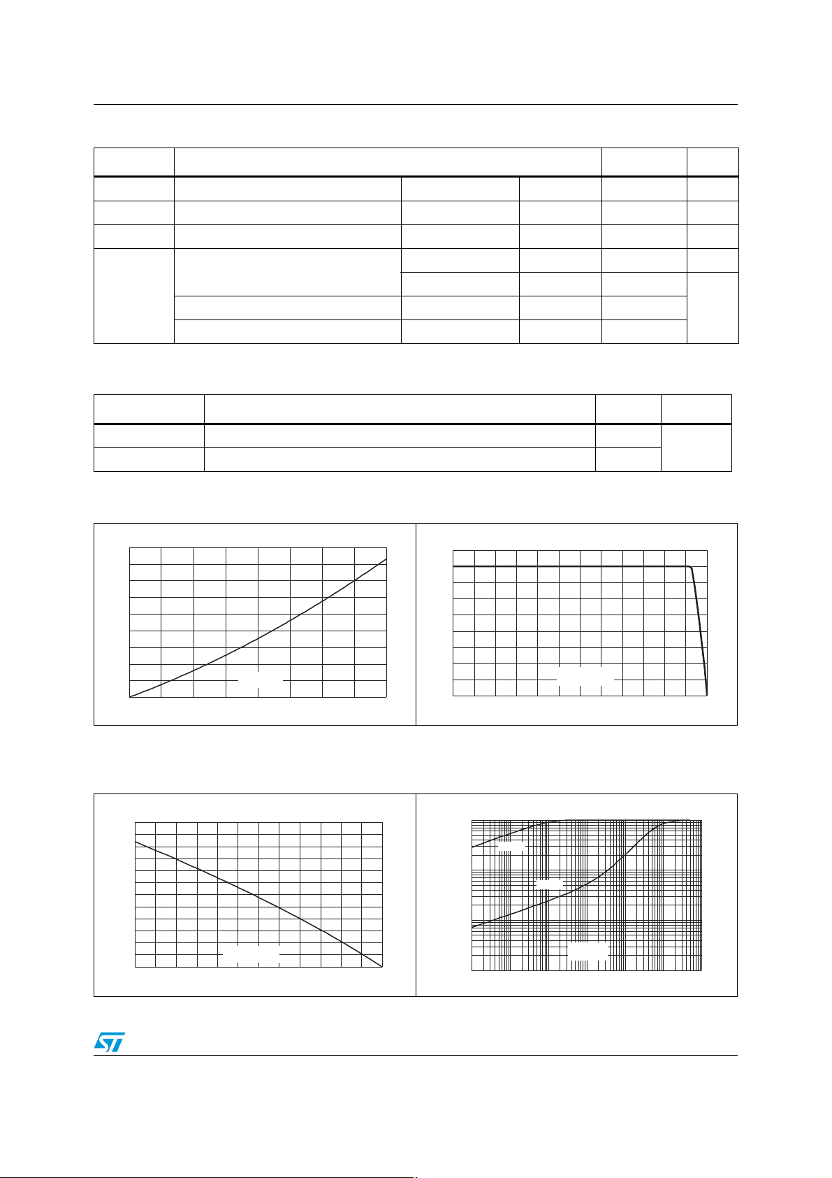
Figure 1. Maximum power dissipation versus
Junction to case (AC) 2.20
Junction to ambient 60
Figure 2. On-state rms current versus case
on-state rms current (full cycle)
temperature (full cycle)
°C/W
mAV
P(W)
4
3
2
1
I
(A)
T(RMS)
0
01234
Figure 3. On-state rms current versus
ambient temperature (free air
convection, full cycle)
I
T(RMS)
3.0
2.5
2.0
1.5
1.0
0.5
0.0
0 25 50 75 100 125 150
Ta(°C)
I
(A)
T(RMS)
4
3
2
1
0
0 25 50 75 100 125 150
TC(°C)
Figure 4. Relative variation of thermal
impedance, versus pulse duration
K=[Zth/Rth]
1.E+00
Zth(j-c)
1.E-01
Zth(j-a)
1.E-02
tp(s)
1.E-03
1.E-03 1.E-02 1.E-01 1.E+00 1.E+01 1.E+02 1.E+03
Doc ID 15712 Rev 1 3/9
 Loading...