

®
T1235H
SNUBBERLESS™ HIGH TEMPERATURE
Table 1: Main Features
Symbol Value Unit
I
T(RMS)
V
DRM/VRRM
I
GT (Q1)
12 A
600 V
35 mA
DESCRIPTION
Specifically designed for use in high temperature
environment (found in hot appliances such as
cookers, ovens, hobs, electric heaters, coffee machines...), the new 12 Amps T1235H triacs provide
an enhanced performance in terms of power loss
and thermal dissipation. This allows for optimization of the heatsinking dimensioning, leading to
space and cost effectivness when compared to
electro-mechnical solutions.
Based on ST snubberless technology, they offer
high commutation switching capabilities and high
noise immunity levels. And, thanks to their clip assembly technique, they provide a superior performance in surge current handling.
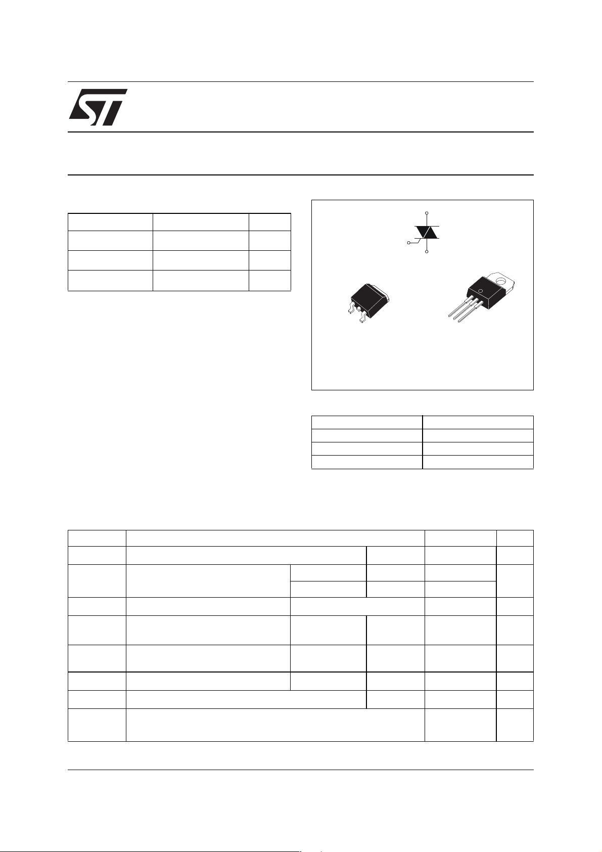
12A TRIACS
A2
G
A1
A2
A1
A2
G
D2PA K
(T1235H-600G)
Table 2: Order Codes
Part Number Marking
T1235H-600G T1235H600G
T1235H-600G-TR T1235H600G
T1235H-600TRG T1235H600T
A1
A2
G
TO-220AB
(T1235H-600T)
A2
Table 3: Absolute Maximum Ratings
Symbol Parameter Value Unit
= 135°C
I
T(RMS)
I
TSM
²
I
tI
dI/dt
V
DSM/VRSM
I
GM
P
G(AV)
T
stg
T
j
RMS on-state current (full sine wave)
Non repetitive surge peak on-state
current (full cycle, T
²
t Value for fusing
initial = 25°C)
j
Critical rate of rise of on-state
current I
= 2 x IGT , tr ≤ 100 ns
G
Non repetitive surge peak off-state
voltage
Peak gate current
Average gate power dissipation
Storage junction temperature range
Operating junction temperature range
F = 50 Hz t = 20 ms 140
F = 60 Hz t = 16.7 ms 145
= 10 ms
t
p
F = 120 Hz
= 10 ms Tj = 25°C 700
t
p
t
= 20 µs Tj = 150°C
p
REV. 6February 2006
T
c
T
= 150°C
j
T
= 150°C
j
12 A
112
50 A/µs
4A
1W
- 40 to + 150
- 40 to + 150
A
°C
A
²
s
V
1/8
T1235H
Tables 4: Electrical Characteristics (Tj = 25°C, unless otherwise specified)
Symbol Test Conditions Quadrant Value Unit
I
(1)
GT
V
GT
V
GD
(2) IT = 100 mA
I
H
I
L
dV/dt (2)
(dI/dt)c (2)
= 12 V RL = 33 Ω
V
D
VD = V
IG = 1.2 I
V
= 67 %V
D
RL = 3.3 kΩ Tj = 150°C
DRM
GT
gate open Tj = 150°C
DRM
Without snubber T
= 150°C
j
Table 5: Static Characteristics
Symbol Test Conditions Value Unit
V
(2) ITM = 17 A tp = 380 µs Tj = 25°C
T
V
(2)
to
(2)
R
d
Threshold voltage
Dynamic resistance
Tj = 150°C
Tj = 150°C
Tj = 25°C
V
= V
I
DRM
I
RRM
Note 1: minimum IGT is guaranted at 10% of IGT max.
Note 2: for both polarities of A2 referenced to A1.
DRM
V
DRM/VRRM
(at mains peak voltage)
RRM
= 400V
= 150°C
T
j
Tj = 150°C
I - II - III MAX. 35 mA
I - II - III MAX. 1.3 V
I - II - III MIN. 0.15 V
MAX. 35 mA
I - III
50
MAX.
II 80
MIN. 300 V/µs
MIN. 5.3 A/ms
MAX. 1.55 V
MAX. 0.80 V
MAX. 25 mΩ
5µA
MAX.
5.5
3.5
mA
mA
Table 6: Thermal resistance
Symbol Parameter Value Unit
2
D
R
th(j-c)
Junction to case (AC)
PAK
1.2 °C/W
TO-220AB
R
th(j-a)
Junction to ambient
S = 1 cm
²D2
PAK
45
TO-220AB 60
S = Copper surface under tab.
2/8
°C/W
T1235H
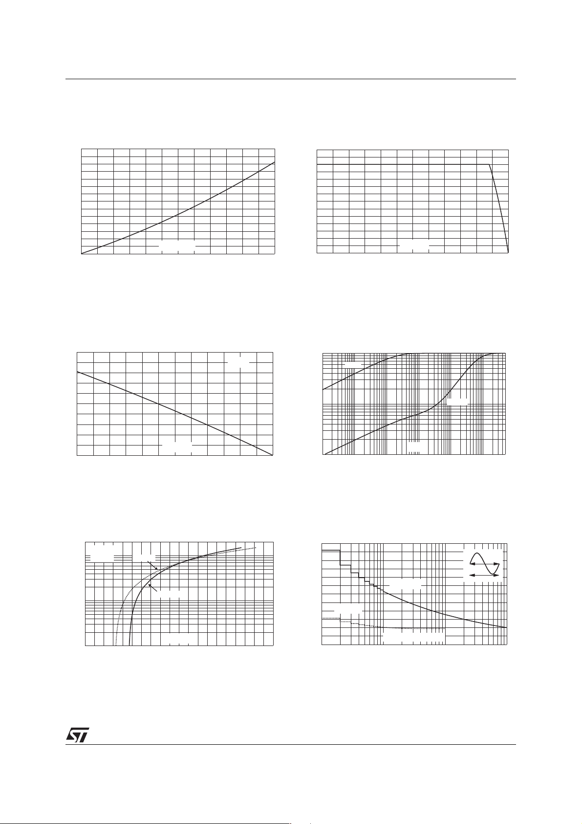
Figure 1: Maximum power dissipation versus
RMS on-state current (full cycle)
P(W)
14
12
10
8
6
4
2
0
024681012
I (A)
T(RMS)
Figure 3: RMS on-state current versus ambient
temperature (printed circuit board FR4, copper
thickness: 35µm) (full cycle)
I (A)
T(RMS)
5
4
2
DPAK
(S=1cm )
2
Figure 2: RMS on-state current versus case
temperature (full cycle)
I (A)
T(RMS)
14
12
10
8
6
4
2
0
0 25 50 75 100 125 150
T (°C)
C
Figure 4: Relative variation of thermal
impedance versus pulse duration
1.00
K=[Z /R
th th
Z
]
th(j-c)
3
2
1
T (°C)
0
0 25 50 75 100 125 150
C
Figure 5: On-state characteristics (maximum
values)
I (A)
TM
200
T max.
j
V = 0.85V
to
100
R = 50 m
d
10
1
0.0 0.5 1.0 1.5 2.0 2.5 3.0 3.5 4.0 4.5 5.0
T=jT max.
Ω
j
T = 25°Cj.
V (V)
TM
Z
0.10
t (s)
0.01
1E-3 1E-2 1E-1 1E+0 1E+1 1E+2 5E+2
p
th(j-a)
Figure 6: Surge peak on-state current versus
number of cycles
I (A)
TSM
150
125
100
75
Repetitive
50
25
T =135°C
C
0
1 10 100 1000
Non repetitive
T initial=25°C
j
Number of cycles
t=20ms
One cycle
3/8
 Loading...