

STZ150NF55T
N-CHANNEL TEMPERATURE SENSING 55V - P²PAK
SAFeFET™ MOSFET
DATA BRIEF
General features
Type
STZ150NF55T 55 V <9 mΩ 40 A(1)
■ INTEGRATED ESD PROTECTION
■ INTEGRATED TEMPERAT UR E SENSIN G
■ STANDARD VGS(th) LEVEL
■ 175°C JUNCTION TEMPERATURE
V
DSSS
R
DS(on)
I
Applications
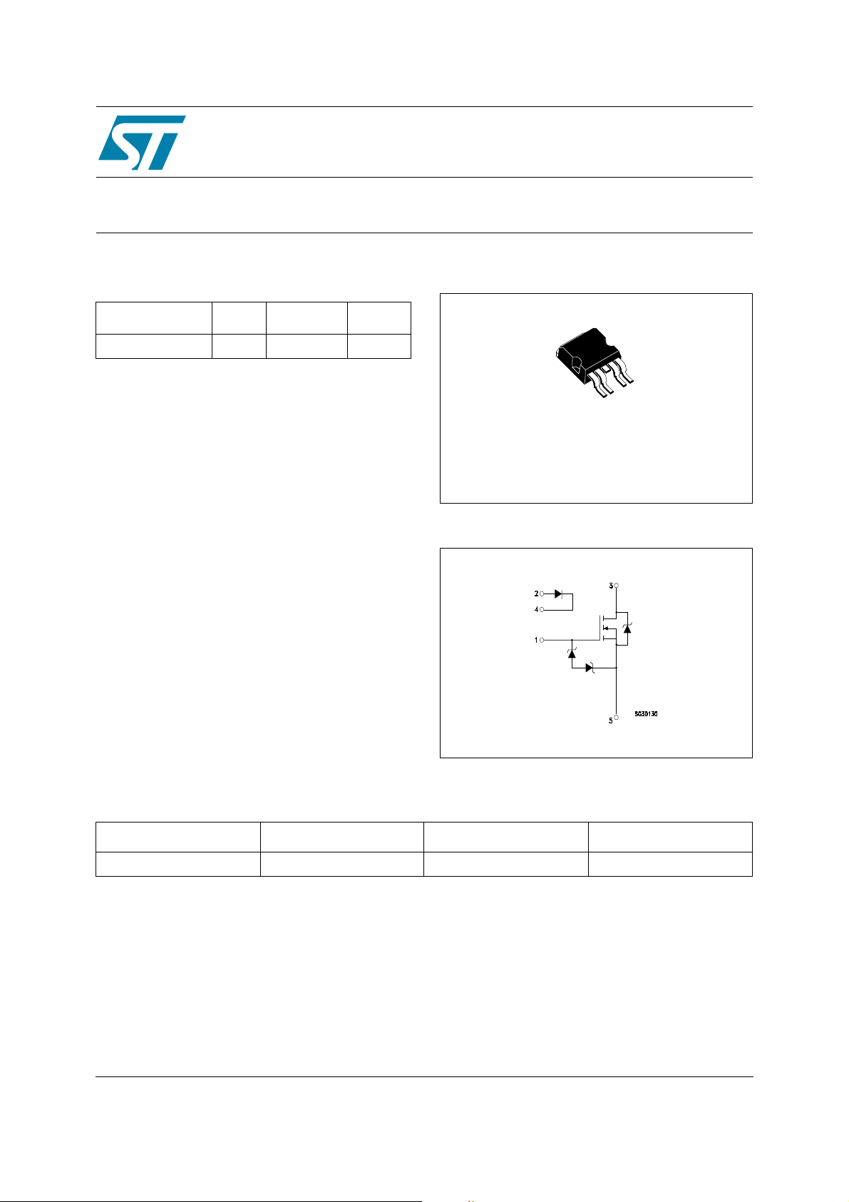
Package
D
5
1
P²PAK
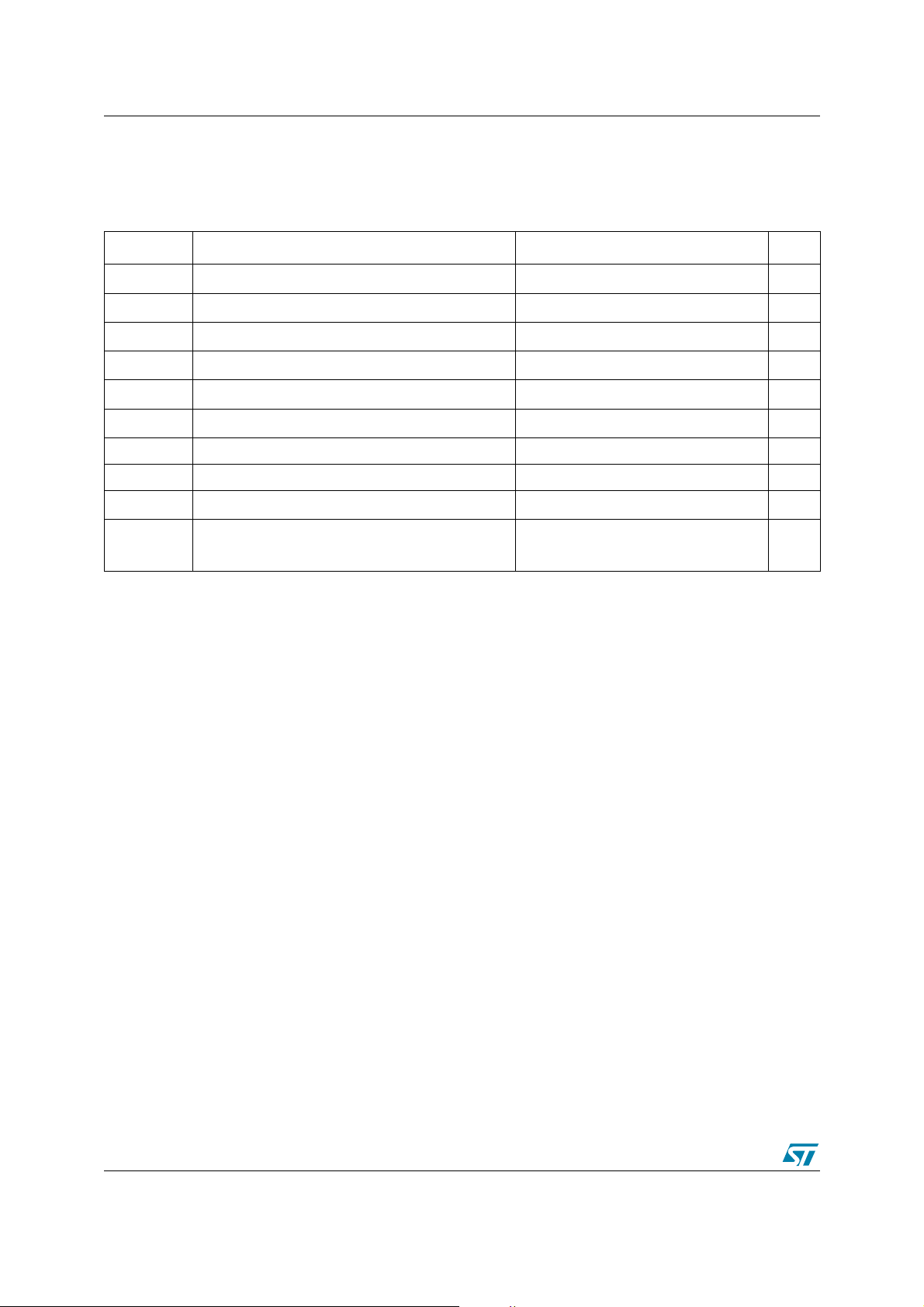
Internal schematic diagram
■ HIGH CURRENT SWITCHING
Order codes
Sales Type Marking Package Packa ging
STZ150NF55T Z150NF55T P²PAK TAPE & REEL
Rev 1
July 2005 1/7
www.st.com
7
1 Absolute maximum ratings STZ150NF55T
1 Absolute maximum ratings
Table 1. Absolute maximum ratings
Symbol Parameter Value Unit
V
DS
V
GS
ID Note 1 Drain Current (conti nuous) at TC = 25°C
I
Note 1 Drain Current (conti nuous) at TC = 100°C
D
I
DM
P
TOT
Drain-Source Voltage (VGS = 0)
55 V
Gate-Source Voltage ± 18 V
40 A
40 A
Drain Current (pulsed ) 160 A
Total Dissipation at TC = 25°C
250 W
Derating Factor 1.67 W/°C
Vesd(G-S) G-S ESD (HBM C=100pF, R=1.5kΩ) >4 kV
E
AS
T
T
stg
Single Pulse Avalanche Energy TBD mJ
Operating Junction Temperature
j
Storage Temperature
-55 to 175 °C
2/7
STZ150NF55T 2 Electrical characteristics
2 Electrical characteristics
(T
= 25 °C unless otherwise specified)
CASE
Table 2. On/Off
Symbol Parameter Test Conditions Min. Typ. Max. Unit
V
(BR)DSS
I
DSS
I
GSS
V
GS(th)
R
DS(on)
V
F
(1) Limited by wire bonding
Drain-Source Breakdown
Voltage
Zero Gate Voltage Drain
Current (V
Gate Body Leakage Current
= 0)
(V
DS
Gate Threshold Voltage
St ati c Drai n-Source On
Resistance
Temperature Sense diode
forward voltage
GS
= 0)
I
= 250µA, VGS= 0
D
= Max Ra ting,
V
DS
= ±15V, V
V
GS
V
= VGS, ID = 250 µA
DS
V
= 10 V, ID= 20 A
GS
I
=250µA
f
DS
= 0
55 V
10 µA
10 µA
24V
9mΩ
3.5 V
3/7

3 Package mechani cal data STZ150NF55T
3 Package m echanical data
In order to meet environmental requirements, ST offers these devices in ECOPACK®
packages. These packages have a Lead-free second level interconnect . The category of
second level interconnect is marked on the package and on the inner box label, in compliance
with JEDEC Standard JESD97. The maximum ratings related to soldering conditions are also
marked on the inner box label. ECOPACK is an ST trademark. ECOPACK specifications are
available at: www.st.com
4/7

STZ150NF55T 3 Package mechanical data
PENTAWATT SMD (P2PAK) MECHANICAL DATA
DIM.
MIN. TYP. MAX. MIN. TYP. MAX.
A 4.30 4.80 0.169 0.188
A2 0.03 0.23 0.001 0.009
C 1.17 1.37 0.046 0.053
D 2.40 2.80 0.094 0.110
D1 8.95 9.35 0.352 0.368
E 0.35 0.55 0.013 0.021
F 0.80 1.05 0.031 0.041
G 3.20 3.60 0.125 0.141
G1 6.60 7.00 0.259 0.275
H2 10.40 0.409
L 13.59 14.39 0.535 0.566
L2 1.27 1.40 0.05 0.055
L3 1.30 1.70 0.051 0.066
R0.30
V2 0 d 8 d
mm inch
PO1OL4
5/7

4 Revision Hist ory STZ150NF55T
4 Revision History
Date Revision Changes
22-Jul-2005 1 Initial release.
6/7

STZ150NF55T 4 Revision History
Information furnished is believed to be accurate and reliable. However, STMicroelectronics assumes no responsibility for the consequences
of use of such information nor for any infringement of patents or other rights of third parties which may result from its use. No license is granted
by implic ation or o th erwise under any patent or patent rights of STM i croelectronics. Sp ecifications menti oned in th i s publicati on are subject
to change without notice. This publication supersedes and replaces all information previously supplied. STMicroelectronics products are not
authoriz ed for use as cri t ic al componen t s i n l i fe support devices or syst em s without ex press written approval of STMicro el ectronics.
The ST logo is a registered t rademark of ST M i croelectr oni cs.
All other nam es are the property of th ei r respectiv e owners
© 2005 STMi croelectronics - All rights reserv ed
STMicroelectron ics group of co m panies
Austra l i a - Be l gi um - Brazil - Canada - Chi na - Czech Republic - Fi nl and - Franc e - Germany - Ho ng K ong - India - Isr ael - Italy - Japan -
Malaysi a - M al ta - Morocco - Singapore - Spain - Sweden - Switzerland - United Kin gdom - United States of America
www.st.com
7/7
 Loading...