

ST STW82100B User Manual
RF down converter with embedded integer-N synthesizer
Features
■ High linearity:
– IIP3: +25.5 dBm
– 2FRF-2FLO spurious rejection: 77 dBc
■ Noise figure:
– NF: 10.5 dB
■ Conversion gain
– CG: 8 dB
■ RF range: 1620 MHz to 2400 MHz
■ Wide IF amplifier frequency range: 70 MHz to
400 MHz
■ Integrated RF balun with internal matching
■ Dual differential integrated VCOs with
automatic center frequency calibration:
– LOA: 1650 to 1950 MHz
– LOB: 2050 to 2370 MHz
■ Embedded integer-N synthesizer
– Dual modulus programmable prescaler
(16/17 or 19/20)
– Programmable reference frequency divider
(10 bits)
– Adjustable charge pump current
– Digital lock detector
– Excellent integrated phase noise
– Fast lock time: 150 µs
■ Integrated DAC with dual current output
■ Supply: 3.3 V and 5 V analog,
3.3 V Digital
■ Dual digital bus interface: SPI and I
mode) with 3 bit programmable address
(1101A
■ Process: 0.35 µm BICMOS SiGe
■ Operating temperature range -40 to +85
■ 44-lead exposed pad VFQFPN
2A1A0
)
package7x7x1.0 mm
2
C bus (fast
o
C
STW82100B
Datasheet − production data
VFQFPN-44
Applications
■ Cellular infrastructure equipment:
– IF sampling receivers
– Digital PA linearization loops
■ Other wireless communication systems.
Table 1. Device summary
Part number Package Packaging
STW82100B VFQFPN-44 Tray
STW82100BTR VFQFPN-44 Tape and reel
Description
The STMicroelectronics STW82100B is an
integrated down converter providing 8 dB of gain,
10.5 dB NF, and a very high input linearity by
means of its passive mixer.
Embedding two wide band auto calibrating VCOs
and an integer-N synthesizer, the STW82100B is
suitable for both Rx and Tx requirements for
Cellular infrastructure equipment.
The integrated RF balun and internal matching
permit direct 50 ohm single-ended interface to RF
port. The IF output is suitable for driving 200-ohm
impedance filters.
By embedding a DAC with dual current output to
drive an external PIN diode attenuator, the
STW82100B replaces several costly discrete
components and offers a significant footprint
reduction.
The STW82100B device is designed with
STMicroelectronics advanced 0.35 µm
SiGe process. Its performance is specified over a
-40 °C to +85 °C temperature range.
May 2012 Doc ID 018355 Rev 5 1/67
This is information on a product in full production.
www.st.com
1

Contents STW82100B
Contents
1 Block diagram . . . . . . . . . . . . . . . . . . . . . . . . . . . . . . . . . . . . . . . . . . . . . . 7
2 Pin description . . . . . . . . . . . . . . . . . . . . . . . . . . . . . . . . . . . . . . . . . . . . . 8
3 Absolute maximum ratings . . . . . . . . . . . . . . . . . . . . . . . . . . . . . . . . . . 11
4 Operating conditions . . . . . . . . . . . . . . . . . . . . . . . . . . . . . . . . . . . . . . . 12
5 Test conditions . . . . . . . . . . . . . . . . . . . . . . . . . . . . . . . . . . . . . . . . . . . . 14
6 Electrical characteristics . . . . . . . . . . . . . . . . . . . . . . . . . . . . . . . . . . . . 15
7 Typical performance characteristics . . . . . . . . . . . . . . . . . . . . . . . . . . . 20
8 General description . . . . . . . . . . . . . . . . . . . . . . . . . . . . . . . . . . . . . . . . . 23
8.1 Circuit description . . . . . . . . . . . . . . . . . . . . . . . . . . . . . . . . . . . . . . . . . . . 23
8.1.1 Reference input stage . . . . . . . . . . . . . . . . . . . . . . . . . . . . . . . . . . . . . . 23
8.1.2 Reference divider . . . . . . . . . . . . . . . . . . . . . . . . . . . . . . . . . . . . . . . . . . 24
8.1.3 Prescaler . . . . . . . . . . . . . . . . . . . . . . . . . . . . . . . . . . . . . . . . . . . . . . . . 24
8.1.4 A and B counters . . . . . . . . . . . . . . . . . . . . . . . . . . . . . . . . . . . . . . . . . . 24
8.1.5 Phase frequency detector (PFD) . . . . . . . . . . . . . . . . . . . . . . . . . . . . . . 25
8.1.6 Lock detect . . . . . . . . . . . . . . . . . . . . . . . . . . . . . . . . . . . . . . . . . . . . . . 26
8.1.7 Mute until lock . . . . . . . . . . . . . . . . . . . . . . . . . . . . . . . . . . . . . . . . . . . . 26
8.1.8 Charge pump . . . . . . . . . . . . . . . . . . . . . . . . . . . . . . . . . . . . . . . . . . . . . 26
8.1.9 Voltage controlled oscillators . . . . . . . . . . . . . . . . . . . . . . . . . . . . . . . . . 27
8.1.10 Output stage . . . . . . . . . . . . . . . . . . . . . . . . . . . . . . . . . . . . . . . . . . . . . 30
8.1.11 External VCO buffer . . . . . . . . . . . . . . . . . . . . . . . . . . . . . . . . . . . . . . . . 30
8.1.12 Mixer and IF amplifier . . . . . . . . . . . . . . . . . . . . . . . . . . . . . . . . . . . . . . 31
8.1.13 Dual output current DAC . . . . . . . . . . . . . . . . . . . . . . . . . . . . . . . . . . . . 32
2/67 Doc ID 018355 Rev 5

STW82100B Contents
9 I2C bus interface . . . . . . . . . . . . . . . . . . . . . . . . . . . . . . . . . . . . . . . . . . . 33
9.1 I2C general features . . . . . . . . . . . . . . . . . . . . . . . . . . . . . . . . . . . . . . . . . 33
9.1.1 Data validity . . . . . . . . . . . . . . . . . . . . . . . . . . . . . . . . . . . . . . . . . . . . . . 33
9.1.2 START and STOP conditions . . . . . . . . . . . . . . . . . . . . . . . . . . . . . . . . . 34
9.1.3 Byte format and acknowledge . . . . . . . . . . . . . . . . . . . . . . . . . . . . . . . . 34
9.1.4 Device addressing . . . . . . . . . . . . . . . . . . . . . . . . . . . . . . . . . . . . . . . . . 35
9.1.5 Single-byte write mode . . . . . . . . . . . . . . . . . . . . . . . . . . . . . . . . . . . . . 35
9.1.6 Multi-byte write mode . . . . . . . . . . . . . . . . . . . . . . . . . . . . . . . . . . . . . . . 35
9.1.7 Current byte address read . . . . . . . . . . . . . . . . . . . . . . . . . . . . . . . . . . . 35
9.2 I2C timing specifications . . . . . . . . . . . . . . . . . . . . . . . . . . . . . . . . . . . . . . 36
9.2.1 Data and clock timing specification . . . . . . . . . . . . . . . . . . . . . . . . . . . . 36
9.2.2 I
9.2.3 I
9.3 I2C registers . . . . . . . . . . . . . . . . . . . . . . . . . . . . . . . . . . . . . . . . . . . . . . . 38
9.3.1 I2C register summary . . . . . . . . . . . . . . . . . . . . . . . . . . . . . . . . . . . . . . . 38
9.3.2 I
2
C START and STOP timing specification . . . . . . . . . . . . . . . . . . . . . . 36
2
C acknowledge timing specification . . . . . . . . . . . . . . . . . . . . . . . . . . 37
2
C register definitions . . . . . . . . . . . . . . . . . . . . . . . . . . . . . . . . . . . . . . 39
9.4 Device calibration through the I2C interface . . . . . . . . . . . . . . . . . . . . . . . 45
9.4.1 VCO calibration procedure (I2C interface) . . . . . . . . . . . . . . . . . . . . . . . 45
9.4.2 Power ON sequence (I
9.4.3 VCO calibration auto-restart procedure (I
2
C interface) . . . . . . . . . . . . . . . . . . . . . . . . . . . . 45
2
C interface) . . . . . . . . . . . . . 46
10 SPI digital interface . . . . . . . . . . . . . . . . . . . . . . . . . . . . . . . . . . . . . . . . . 47
10.1 SPI general features . . . . . . . . . . . . . . . . . . . . . . . . . . . . . . . . . . . . . . . . . 47
10.2 SPI timing specification . . . . . . . . . . . . . . . . . . . . . . . . . . . . . . . . . . . . . . 49
10.2.1 Data, clock and load timing . . . . . . . . . . . . . . . . . . . . . . . . . . . . . . . . . . 49
10.3 SPI registers . . . . . . . . . . . . . . . . . . . . . . . . . . . . . . . . . . . . . . . . . . . . . . . 50
10.3.1 SPI register summary . . . . . . . . . . . . . . . . . . . . . . . . . . . . . . . . . . . . . . 50
10.3.2 SPI register definitions . . . . . . . . . . . . . . . . . . . . . . . . . . . . . . . . . . . . . . 50
10.4 Device calibration through the SPI interface . . . . . . . . . . . . . . . . . . . . . . 53
10.4.1 VCO calibration procedure (SPI interface) . . . . . . . . . . . . . . . . . . . . . . . 53
10.4.2 Power ON sequence (SPI interface) . . . . . . . . . . . . . . . . . . . . . . . . . . . 53
10.4.3 VCO calibration auto-restart procedure (SPI interface) . . . . . . . . . . . . . 54
Doc ID 018355 Rev 5 3/67

Contents STW82100B
11 Application information . . . . . . . . . . . . . . . . . . . . . . . . . . . . . . . . . . . . . 55
11.1 Application circuit . . . . . . . . . . . . . . . . . . . . . . . . . . . . . . . . . . . . . . . . . . . 55
11.2 Standard Mode Operation . . . . . . . . . . . . . . . . . . . . . . . . . . . . . . . . . . . . 57
11.3 Diversity mode operation with same LO frequency . . . . . . . . . . . . . . . . . 58
11.4 Diversity mode operation with different LO frequencies . . . . . . . . . . . . . . 59
11.5 External VCO standard mode operation . . . . . . . . . . . . . . . . . . . . . . . . . 60
11.6 External VCO diversity mode operation with same LO . . . . . . . . . . . . . . 61
12 Evaluation kit . . . . . . . . . . . . . . . . . . . . . . . . . . . . . . . . . . . . . . . . . . . . . . 62
13 Package mechanical data . . . . . . . . . . . . . . . . . . . . . . . . . . . . . . . . . . . . 63
14 Revision history . . . . . . . . . . . . . . . . . . . . . . . . . . . . . . . . . . . . . . . . . . . 65
4/67 Doc ID 018355 Rev 5

STW82100B List of tables
List of tables
Table 1. Device summary . . . . . . . . . . . . . . . . . . . . . . . . . . . . . . . . . . . . . . . . . . . . . . . . . . . . . . . . . . 1
Table 2. Pin list . . . . . . . . . . . . . . . . . . . . . . . . . . . . . . . . . . . . . . . . . . . . . . . . . . . . . . . . . . . . . . . . . . 9
Table 3. Absolute maximum ratings . . . . . . . . . . . . . . . . . . . . . . . . . . . . . . . . . . . . . . . . . . . . . . . . . 11
Table 4. Operating conditions . . . . . . . . . . . . . . . . . . . . . . . . . . . . . . . . . . . . . . . . . . . . . . . . . . . . . . 12
Table 5. Digital logic levels . . . . . . . . . . . . . . . . . . . . . . . . . . . . . . . . . . . . . . . . . . . . . . . . . . . . . . . . 13
Table 6. Down converter mixer and IF amplifier electrical characteristics . . . . . . . . . . . . . . . . . . . . 15
Table 7. Pin diode attenuator driver (dual output current DAC) electrical characteristics. . . . . . . . . 16
Table 8. Integer-N synthesizer electrical characteristics. . . . . . . . . . . . . . . . . . . . . . . . . . . . . . . . . . 17
Table 9. Phase noise performance . . . . . . . . . . . . . . . . . . . . . . . . . . . . . . . . . . . . . . . . . . . . . . . . . . 19
Table 10. Current values for CPSEL[2:0] selection . . . . . . . . . . . . . . . . . . . . . . . . . . . . . . . . . . . . . . 26
Table 11. VCOA performance against amplitude setting (frequency = 3.6 GHz) . . . . . . . . . . . . . . . . 30
Table 12. VCOB performance against amplitude setting (frequency = 4.3 GHz) . . . . . . . . . . . . . . . . 30
Table 13. Suggested CAP[2:0] values for LO Frequency range mixer . . . . . . . . . . . . . . . . . . . . . . . . 31
Table 14. Linearity performance against IFAMP[1:0] configuration (typical condition) . . . . . . . . . . . . 32
Table 15. I
Table 16. I
Table 17. I
Table 18. I
Table 19. Address decoder and outputs . . . . . . . . . . . . . . . . . . . . . . . . . . . . . . . . . . . . . . . . . . . . . . . 48
Table 20. SPI timing parameters . . . . . . . . . . . . . . . . . . . . . . . . . . . . . . . . . . . . . . . . . . . . . . . . . . . . 49
Table 21. SPI register list . . . . . . . . . . . . . . . . . . . . . . . . . . . . . . . . . . . . . . . . . . . . . . . . . . . . . . . . . . 50
Table 22. Application circuit component values . . . . . . . . . . . . . . . . . . . . . . . . . . . . . . . . . . . . . . . . . 56
Table 23. Evaluation kit order code . . . . . . . . . . . . . . . . . . . . . . . . . . . . . . . . . . . . . . . . . . . . . . . . . . 62
Table 24. VFQFPN-44 package dimensions . . . . . . . . . . . . . . . . . . . . . . . . . . . . . . . . . . . . . . . . . . . 64
Table 25. Document revision history . . . . . . . . . . . . . . . . . . . . . . . . . . . . . . . . . . . . . . . . . . . . . . . . . 65
2
C data and clock timing parameters. . . . . . . . . . . . . . . . . . . . . . . . . . . . . . . . . . . . . . . . . 36
2
C START and STOP timing parameters . . . . . . . . . . . . . . . . . . . . . . . . . . . . . . . . . . . . . 37
2
C acknowledge timing parameters. . . . . . . . . . . . . . . . . . . . . . . . . . . . . . . . . . . . . . . . . . 37
2
C register list . . . . . . . . . . . . . . . . . . . . . . . . . . . . . . . . . . . . . . . . . . . . . . . . . . . . . . . . . . 38
Doc ID 018355 Rev 5 5/67

List of figures STW82100B
List of figures
Figure 1. STW82100B block diagram . . . . . . . . . . . . . . . . . . . . . . . . . . . . . . . . . . . . . . . . . . . . . . . . . 7
Figure 2. STW82100B pin configuration . . . . . . . . . . . . . . . . . . . . . . . . . . . . . . . . . . . . . . . . . . . . . . . 8
Figure 3. Conversion gain against RF frequency. . . . . . . . . . . . . . . . . . . . . . . . . . . . . . . . . . . . . . . . 20
Figure 4. Noise figure against RF frequency . . . . . . . . . . . . . . . . . . . . . . . . . . . . . . . . . . . . . . . . . . . 20
Figure 5. IIP3 against RF frequency . . . . . . . . . . . . . . . . . . . . . . . . . . . . . . . . . . . . . . . . . . . . . . . . . 21
Figure 6. 2RF-2LO response against RF frequency . . . . . . . . . . . . . . . . . . . . . . . . . . . . . . . . . . . . . 21
Figure 7. LOA (VCOA div. by 2) closed-loop phase noise at 1.8 GHz
(F
Figure 8. LOB (VCOB div. by 2) closed-loop phase noise at 2.2 GHz
(F
Figure 9. Reference frequency input buffer . . . . . . . . . . . . . . . . . . . . . . . . . . . . . . . . . . . . . . . . . . . . 23
Figure 10. VCO divider diagram . . . . . . . . . . . . . . . . . . . . . . . . . . . . . . . . . . . . . . . . . . . . . . . . . . . . . 25
Figure 11. PFD diagram. . . . . . . . . . . . . . . . . . . . . . . . . . . . . . . . . . . . . . . . . . . . . . . . . . . . . . . . . . . . 25
Figure 12. Loop filter connection . . . . . . . . . . . . . . . . . . . . . . . . . . . . . . . . . . . . . . . . . . . . . . . . . . . . . 27
Figure 13. VCO typical sub-band characteristics. . . . . . . . . . . . . . . . . . . . . . . . . . . . . . . . . . . . . . . . . 28
Figure 14. Data validity waveform . . . . . . . . . . . . . . . . . . . . . . . . . . . . . . . . . . . . . . . . . . . . . . . . . . . . 33
Figure 15. START and STOP condition waveform . . . . . . . . . . . . . . . . . . . . . . . . . . . . . . . . . . . . . . . 34
Figure 16. Byte format and acknowledge waveform . . . . . . . . . . . . . . . . . . . . . . . . . . . . . . . . . . . . . . 34
Figure 17. I
Figure 18. I
Figure 19. I
Figure 20. I
Figure 21. SPI input and output bit order . . . . . . . . . . . . . . . . . . . . . . . . . . . . . . . . . . . . . . . . . . . . . . . 47
Figure 22. SPI data structure . . . . . . . . . . . . . . . . . . . . . . . . . . . . . . . . . . . . . . . . . . . . . . . . . . . . . . . . 48
Figure 23. SPI timing waveforms . . . . . . . . . . . . . . . . . . . . . . . . . . . . . . . . . . . . . . . . . . . . . . . . . . . . . 49
Figure 24. SPI first programming timing . . . . . . . . . . . . . . . . . . . . . . . . . . . . . . . . . . . . . . . . . . . . . . . 54
Figure 25. Typical STW82100B application circuit . . . . . . . . . . . . . . . . . . . . . . . . . . . . . . . . . . . . . . . 55
Figure 26. Standard mode operation . . . . . . . . . . . . . . . . . . . . . . . . . . . . . . . . . . . . . . . . . . . . . . . . . . 57
Figure 27. Diversity mode operation with same LO frequencies . . . . . . . . . . . . . . . . . . . . . . . . . . . . . 58
Figure 28. Diversity mode operation with different LO frequencies . . . . . . . . . . . . . . . . . . . . . . . . . . . 59
Figure 29. External VCO standard mode operation . . . . . . . . . . . . . . . . . . . . . . . . . . . . . . . . . . . . . . . 60
Figure 30. External VCO diversity mode operation with same LO. . . . . . . . . . . . . . . . . . . . . . . . . . . . 61
Figure 31. VFQFPN-44 package outline . . . . . . . . . . . . . . . . . . . . . . . . . . . . . . . . . . . . . . . . . . . . . . . 63
= 200 kHz, ICP = 2 mA) . . . . . . . . . . . . . . . . . . . . . . . . . . . . . . . . . . . . . . . . . . . . . . . . . . . . . . . . 22
STEP
= 200 kHz, ICP = 2 mA) . . . . . . . . . . . . . . . . . . . . . . . . . . . . . . . . . . . . . . . . . . . . . . . . . . . . . . . . 22
STEP
2
C data and clock waveforms . . . . . . . . . . . . . . . . . . . . . . . . . . . . . . . . . . . . . . . . . . . . . . 36
2
C START and STOP timing waveforms . . . . . . . . . . . . . . . . . . . . . . . . . . . . . . . . . . . . . . 36
2
C acknowledge timing waveforms . . . . . . . . . . . . . . . . . . . . . . . . . . . . . . . . . . . . . . . . . . 37
2
C first programming timing . . . . . . . . . . . . . . . . . . . . . . . . . . . . . . . . . . . . . . . . . . . . . . . 46
6/67 Doc ID 018355 Rev 5
STW82100B Block diagram
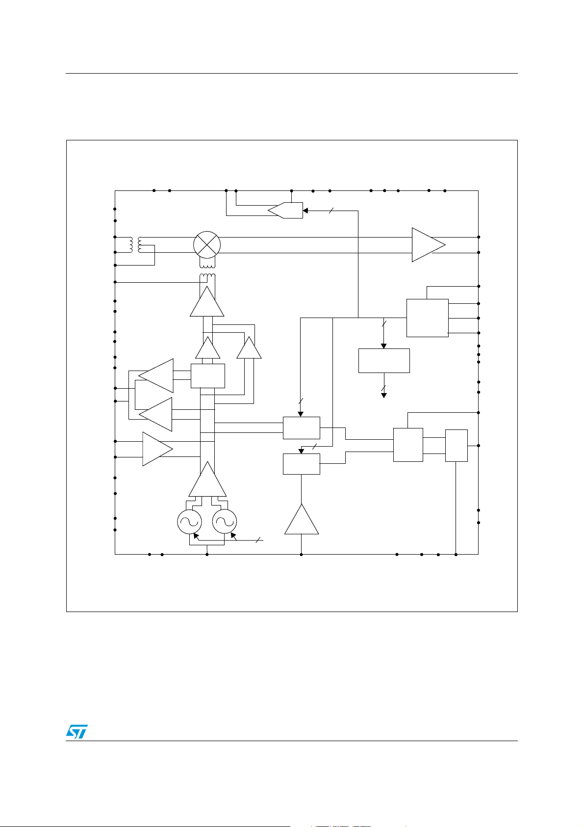
1 Block diagram
Figure 1. STW82100B block diagram
VDD_DAC
VDD_ALC
VSS_ALC
I_PINDRV1
I_PINDRV2
REXT_DAC
VSS_DAC
TEST_ALC
TEST2
TEST1
VDD_IFAMP
VSS_IFAMP
VDD_RFESD
VSS_RFESD
RF_IN
RF_VSS
RF_CT
MIXDRV_CT
VDD_MIXDRV
VSS_MIXDRV
VDD_DIV
VSS_DIV
VDD_OUTBUF
VSS_OUTBUF
OUTBUFN
OUTBUFP
EXTVCO_INP
EXTVCO_INN
VDD_VCO
VSS_VCO
VDD_IO
VSS_IO
LO
OUT
LO/2xLO
OUT
EXT
LO/VCO
BUF
MIX
DRV
DIV2
VCO
BUFF
CAL_VCO
DAC
VCO
divider
REF
divider
BUF
VCO
calibrator
CAL_VCO
PFD
IF
AMP
DBUS
UP
DN
CHP
IF_OUTP
IF_OUTN
DBUS_SEL
SDA/DATA
SCL/CLK
LOAD
ADD0
ADD1
ADD2
VDD_DIG
VSS_DIG
LOCK_DET
ICP
VDD_PLL
VSS_PLL
VDD_PSCBUF
VSS_PSCBUF
VCTRL
REF_CLK
EXT_PD
VSS_CP
VDD_CP
REXT_CP
Doc ID 018355 Rev 5 7/67
Pin description STW82100B
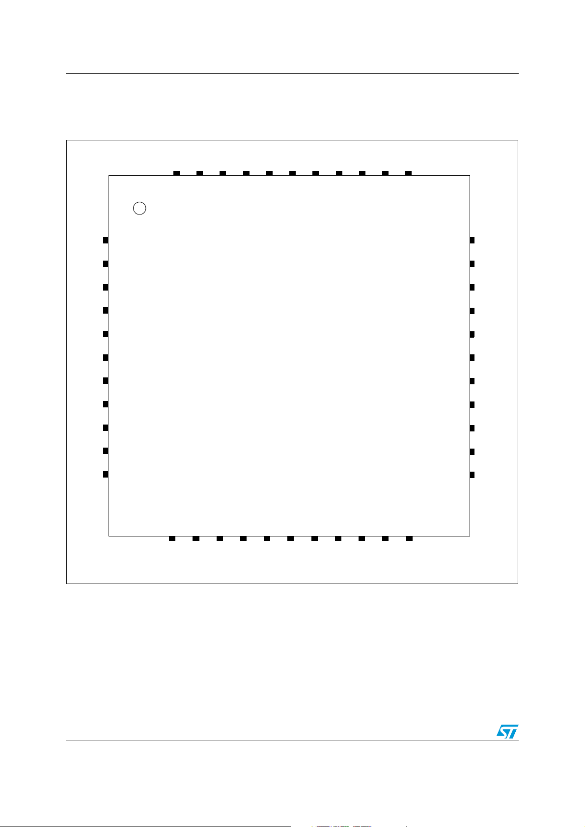
2 Pin description
Figure 2. STW82100B pin configuration
44 43 42 41 40 39 38 37 36 35 34
10
11
1
2
3
4
5
6
7
8
9
VDD_DAC
REXT_DAC
VDD_DIV
VDD_VCO
EXTVCO_INN
EXTVCO_INP
EXT_PD
ADD2
ADD1
ADD0
VDD_IO
RF_IN
RF_CT
VDD_MIXDRV
VDD_ALC
MIXDRV_CT
VDD_RFESD
I_PINDRV1
I_PINDRV2
TEST_ALC
TEST1
TEST2
VDD_IFAMP
IF_OUTP
IF_OUTN
NC
LOAD
33
32
31
30
29
STW82100B
VFQFPN44
SCL/CLK
SDA/DATA
VDD_DIG
DBUS_SEL
VDD_PLL
REF_CLK
28
27
26
25
24
23
VDD_PSCBUF
NC
NC
VDD_OUTBUF
OUTBUFN
OUTBUFP
VCTRL
12 13 14 15 16 17 18 19 20 21 22
8/67 Doc ID 018355 Rev 5
ICP
REXT_CP
VDD_CP
LOCK_DET
STW82100B Pin description
Table 2. Pin list
Pin No Name Description Observation
1 VDD_DAC DAC power supply Vsupply analog1= 3.3 V
2 REXT_DAC External resistance connection for DAC -
3 VDD_DIV Divider by 2 power supply Vsupply analog1= 3.3 V
4 VDD_VCO VCOs and External VCO Buffer power supply Vsupply analog1= 3.3 V
Diversity Slave Mode and External
5 EXTVCO_INN External VCO (LO) negative input
6 EXTVCO_INP External VCO (LO) positive input
7 EXT_PD
8 ADD2 I
9 ADD1 I
10 ADD0 I
Hardware power down:
‘0’ device ON; ‘1’ device OFF
2
CBUS address select pin CMOS Input
2
CBUS address select pin CMOS Input
2
CBUS address select pin CMOS Input
11 VDD_IO Digital IO power supply Vsupply digital = 3.3 V
12 VDD_PSCBUF Prescaler input buffer power supply Vsupply analog1= 3.3 V
13 NC Not connected -
VCO Modes; otherwise it must be
connected to GND
Diversity Slave Mode and External
VCO Modes; otherwise it must be
connected to GND
CMOS Input
14 NC Not connected -
15 VDD_OUTBUF Power supply for LO buffer Vsupply analog1=3.3 V
16 OUTBUFN LO Output buffer negative output Open collector @3.3 V
17 OUTBUFP LO Output buffer positive output Open collector @ 3.3 V
18 VCTRL Control voltage for VCOs -
19 ICP PLL charge pump output -
20 REXT_CP
External resistance connection for PLL charge
pump current
-
21 VDD_CP Power supply for charge pump Vsupply analog1= 3.3 V
22 LOCK_DET Lock detector CMOS Output
23 REF_CLK Reference frequency input -
24 VDD_PLL PLL digital power supply Vsupply analog1= 3.3 V
25 DBUS_SEL Digital Bus Interface select CMOS Input
26 VDD_DIG Power supply for digital bus interface Vsupply digital = 3.3 V
2
27 SDA/DATA I
28 SCL/CLK I
CBUS /SPI data line CMOS Bidir Schmitt triggered
2
CBUS /SPI clock line CMOS Input Schmitt triggered
29 LOAD SPI load line CMOS Input Schmitt triggered
30 NC Not connected -
31 IF_OUTN IF amplifier negative output Open collector @ 5 V
(1)
Doc ID 018355 Rev 5 9/67
Pin description STW82100B
Table 2. Pin list (continued)
Pin No Name Description Observation
32 IF_OUTP IF Amplifier positive output Open collector @ 5 V
33 VDD_IFAMP IF Amplifier power supply Vsupply analog1 = 3.3 V
34 TEST2 Test input 2
35 TEST1 Test input 1
Test purpose only; it must be
connected to GND
Test purpose only; it must be
connected to GND
(1)
36 TEST_ALC Test output
Test purpose only; it must be
connected to GND
37 RF_CT RF balun central tap -
38 RF_IN RF input -
39 VDD_RFESD RF ESD positive rail power supply Vsupply analog1 = 3.3 V
40 MIXDRV_CT Mixer driver balun central tap Vsupply analog2 = 5 V
41 VDD_ALC ALC power supply Vsupply analog1 = 3.3 V
42 VDD_MIXDRV Mixer driver power supply Vsupply analog1 = 3.3 V
43 I_PINDRV1
44 I_PINDRV2
1. Supply voltage @ 3.3 V in low-current mode operation
DAC current output for external PIN Diode
attenuator
DAC current output for external PIN Diode
attenuator
PMOS Open drain
PMOS Open drain
(1)
10/67 Doc ID 018355 Rev 5
STW82100B Absolute maximum ratings
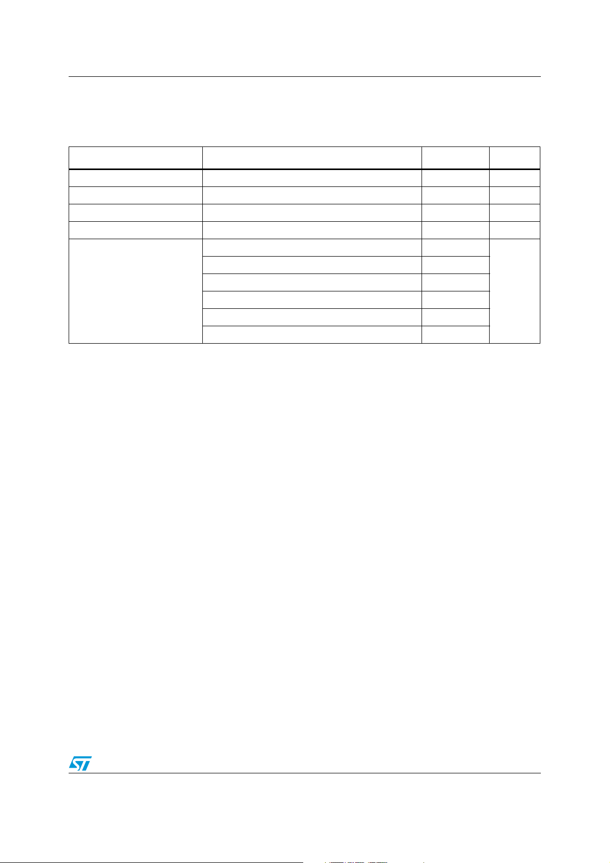
3 Absolute maximum ratings
Table 3. Absolute maximum ratings
Symbol Parameter Values Unit
AVCC1 Analog Supply voltage 0 to 4.6 V
AVCC2 Analog Supply voltage 0 to 6 V
DVCC Digital Supply voltage 0 to 4.6 V
Tstg Storage temperature +150 °C
HBM on pins 16, 17, 31, 32, 37, 40 0.8
HBM on pin 38 1
ESD
(Electro-static discharge)
HBM on all remaining pins 2
kV
CDM-JEDEC Standard on pin 38 0.25
CDM-JEDEC Standard on all remaining pins 0.5
MM 0.2
Doc ID 018355 Rev 5 11/67
Operating conditions STW82100B
4 Operating conditions
Table 4. Operating conditions
Symbol Parameter Test conditions Min Typ Max Unit
AVCC1 Analog Supply voltage - 3.15 3.3 3.45 V
AVCC2 Analog Supply voltage - 4.75 5 5.25 V
DVCC Digital Supply voltage - 3.15 3.3 3.45 V
Standard mode - 130 150 mA
External VCO standard mode - 110 130 mA
I
CC3.3V
Current Consumption at 3.3 V
Diversity slave mode - 105 120 mA
Diversity master mode - 155 180 mA
External VCO diversity master
mode
- 140 160 mA
High current mode at 5 V - 170 195 mA
I
CC5V
T
A
T
J
Θ
JA
Θ
JB
Θ
JC
Ψ
JB
Current Consumption
Low current mode at 3.3 V - 100 115 mA
Operating ambient temperature - -40 85 °C
Maximum junction temperature - - 125 °C
Junction to ambient package thermal
resistance
Junction to board package thermal
resistance
Junction to case package thermal
resistance
Thermal characterization parameter
junction to board
(1)
(1)
(1)
(1)
Multi-layer JEDEC board - 33 - °C/W
Multi-layer JEDEC board - 19 - °C/W
Multi-layer JEDEC board - 3 - °C/W
Multi-layer JEDEC board - 18 - °C/W
Ψ
JT
1. Refer to JEDEC standard JESD 51-12 for a detailed description of the thermal resistances and thermal parameters.
Data here presented are referring to a Multi-layer board according to JEDEC standard.
T
= TA + ΘJA * Pdiss (in order to estimate TJ if ambient temperature TA and dissipated power Pdiss are known)
J
T
= TB + ΨJB * Pdiss (in order to estimate TJ if board temperature TB and dissipated power Pdiss are known)
J
T
= TT + ΨJT * Pdiss (in order to estimate TJ if top case temperature TT and dissipated power Pdiss are known)
J
Thermal characterization parameter
junction to top case
(1)
Multi-layer JEDEC board - 0.3 - °C/W
12/67 Doc ID 018355 Rev 5

STW82100B Operating conditions
Table 5. Digital logic levels
T
Symbol Parameter Test conditions Min Typ Max Unit
Vil Low level input voltage - - - 0.2*Vdd V
Vih High level input voltage - 0.8*Vdd - - V
Vhyst Schmitt trigger hysteresis - 0.8 - - V
Vol Low level output voltage - - - 0.4 V
Voh High level output voltage - 0.85*Vdd - - V
Doc ID 018355 Rev 5 13/67

Test conditions STW82100B
5 Test conditions
Unless otherwise specified the following test conditions are applied:
● Vsupply digital = 3.3 V
● Vsupply analog1 = 3.3 V
● Vsupply analog2 = 5 V
● F
● MIX = 0111
● T ambient = 27 ° C
Refer also to Section 11: Application information.
= 150 MHz
IF
14/67 Doc ID 018355 Rev 5
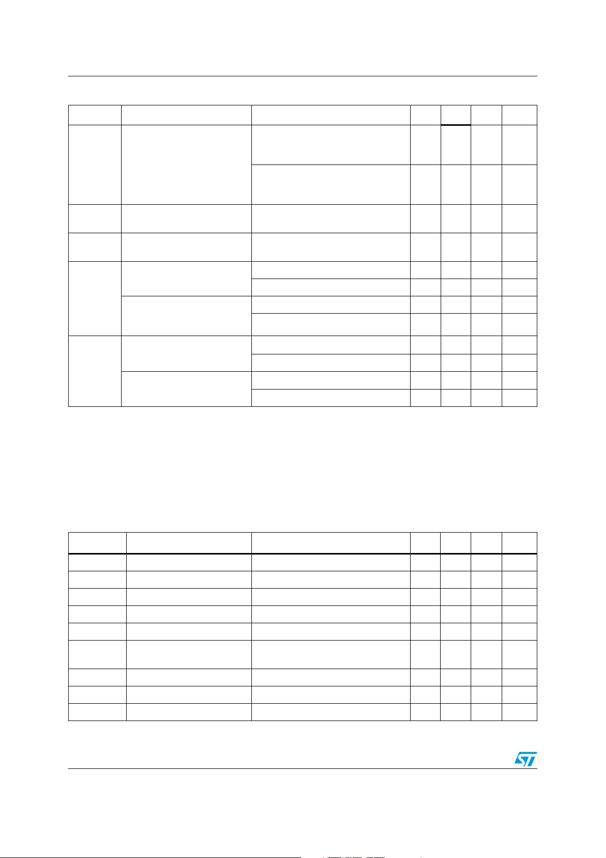
STW82100B Electrical characteristics
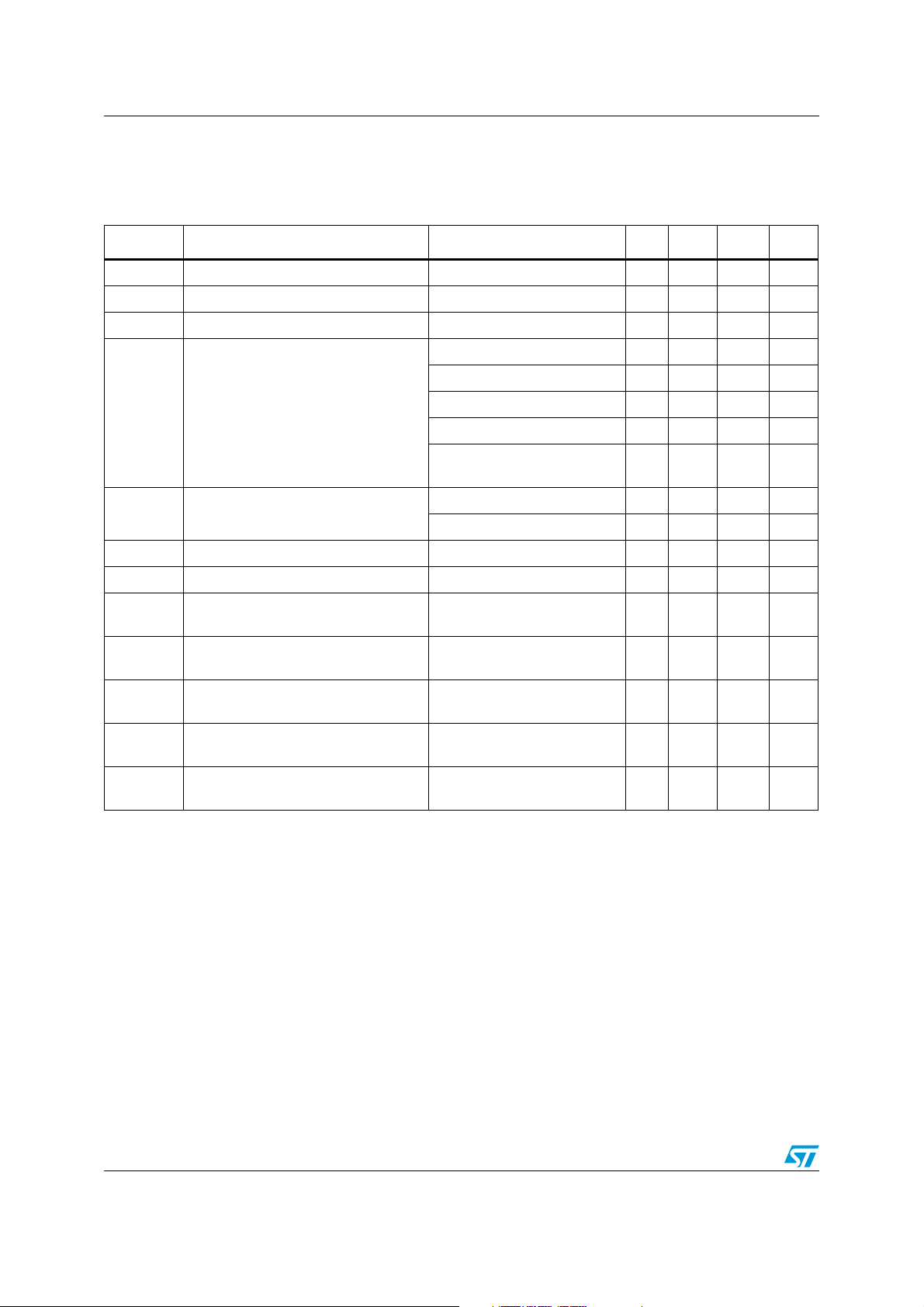
6 Electrical characteristics
Note: Vsupply digital = 3.3 V, Vsupply analog1 = 3.3 V, Vsupply analog2 = 5 V, FRF = 2100 MHz,
F
= 1950 MHz, TA = +25 *C, RF power = 0 dBm, unless otherwise specified.
LO
Table 6. Down converter mixer and IF amplifier electrical characteristics
)
Symbol Parameter Conditions Min Typ Max Unit
F
RF
F
LO
F
IF
CG Power Conversion Gain
CG
ΔT
RF Frequency - 1620 - 2400 MHz
VCOA divided by 2 1650 - 1950 MHz
LO Frequency
VCOB divided by 2 2050 - 2370 MHz
IF Center Frequency
(2)
FIF = ABS(FLO-FRF)70-400MHz
Rin = 50 ohm, Rout = 200 ohm
RFin = 0 dBm
Power Conversion Gain over
Temperature
(3)
T= -40 to +85 °C - ±0.7 - dB
(1)
7.5 8 8.5 dB
IP
1dB
IIP3
IIP3
ΔT
nFRF-nFLOSpurious rejection at IF
Input P1dB
Third-order input intercept
(4)
point
IIP3 variation over
temperature
(3)
(3)
Low current Mode - 8 -
High current Mode 24.5 25.5 -
Low current Mode 18.5 19.5 -
T= -40 to +85 °C - ±0.5 - dB
2F
-2FLO F
RF
F
= 150 MHz
IF
-3FLO F
3F
RF
= 150 MHz
F
IF
RFin
RFin
= -5 dBm,
= -5 dBm,
-77-dBc
-77-dBc
dBm
dBm
High-current mode, MIX = 0011 - 10.5 11 dB
High current Mode - 13.5 -
NF
SSB
Noise figure
Low-current mode, MIX = 0011 - 10.5 11 dB
1xLO - -35 - dBm
- LO to IF Leakage
2xLO -33
- LO to RF Leakage - - -29 - dBm
- RF to IF Isolation - - 58 - dB
RF
IF
RL
RL
RF Return Loss Matched to 50 ohm - 20 - dB
IF Return Loss Matched to 200 ohm - 25 - dB
Maximum deviation from Fc over ±10
MHz. For any Fc within each TX
-
observation path
(5)
Gain Flatness for TX
observation path band.
Maximum deviation from F
over ±30
c
MHz. For any Fc within each TX
-0.05 - +0.05 dB
-0.10 - +0.10 dB
observation path band.
Doc ID 018355 Rev 5 15/67
Electrical characteristics STW82100B
Table 6. Down converter mixer and IF amplifier electrical characteristics
(1)
(continued)
Symbol Parameter Conditions Min Typ Max Unit
Maximum deviation from linear phase
-
Phase Flatness for TX
observation path
(5)
- Gain Flatness for RX path
- Phase Flatness for RX path
Mixer Driver Current
Consumption
ICC
MD
Mixer Driver Current
Consumption (Low Current
Mode)
IFAMP Current Consumption
ICC
IFAM
IFAMP Current Consumption
(Low Current Mode)
at Fc over ±10 MHz. For any Fc within
each TX observation path band.
Maximum deviation from linear phase
at F
over ±30 MHz. For any Fc within
c
each TX observation path band.
Maximum ripple over a 4 MHz band.
(5)
For any F
Maximum ripple over a 4 MHz band.
(5)
For any F
within each RX path band.
c
within each RX path band.
c
3.3 V Supply (pin 41, 42) - 49 - mA
5 V Supply (pin 40) - 60 - mA
3.3 V Supply (pin 41, 42) - 20 - mA
3.3 V Supply (pin 40) - 35 - mA
3.3 V Supply (pin 33) - 10 - mA
5 V Supply (pin 31, 32) - 108 - mA
3.3 V Supply (pin 33) - 6 - mA
3.3 V Supply (pin 31, 32) - 55 - mA
-0.3 - +0.3 deg
-0.7 - +0.7 deg
--0.1
--0.6
dB
pk-pk
deg
pk-pk
1. All linearity and NF performances are intended at maximum LO amplitude (LO_A[1:0]=[11]), tuning capacitors (CAP[2:0])
programmed according to the selected frequency, mixer bias (MIX[3:0]) set to maximize performance and the device
operated in high current mode. The performances of conversion gain, NF and linearity are intended at the SMA connectors
of a typical application board.
2. The IF frequency range supported by the IF Amplifier is from 70 to 400 MHz. The exact IF frequency range supported for a
specific RF frequency can be calculated as F
3. Guaranteed by design and characterization
4. RFin = 0 dBm/tone, RF tone spacing = 5 MHz
5. Guaranteed by design
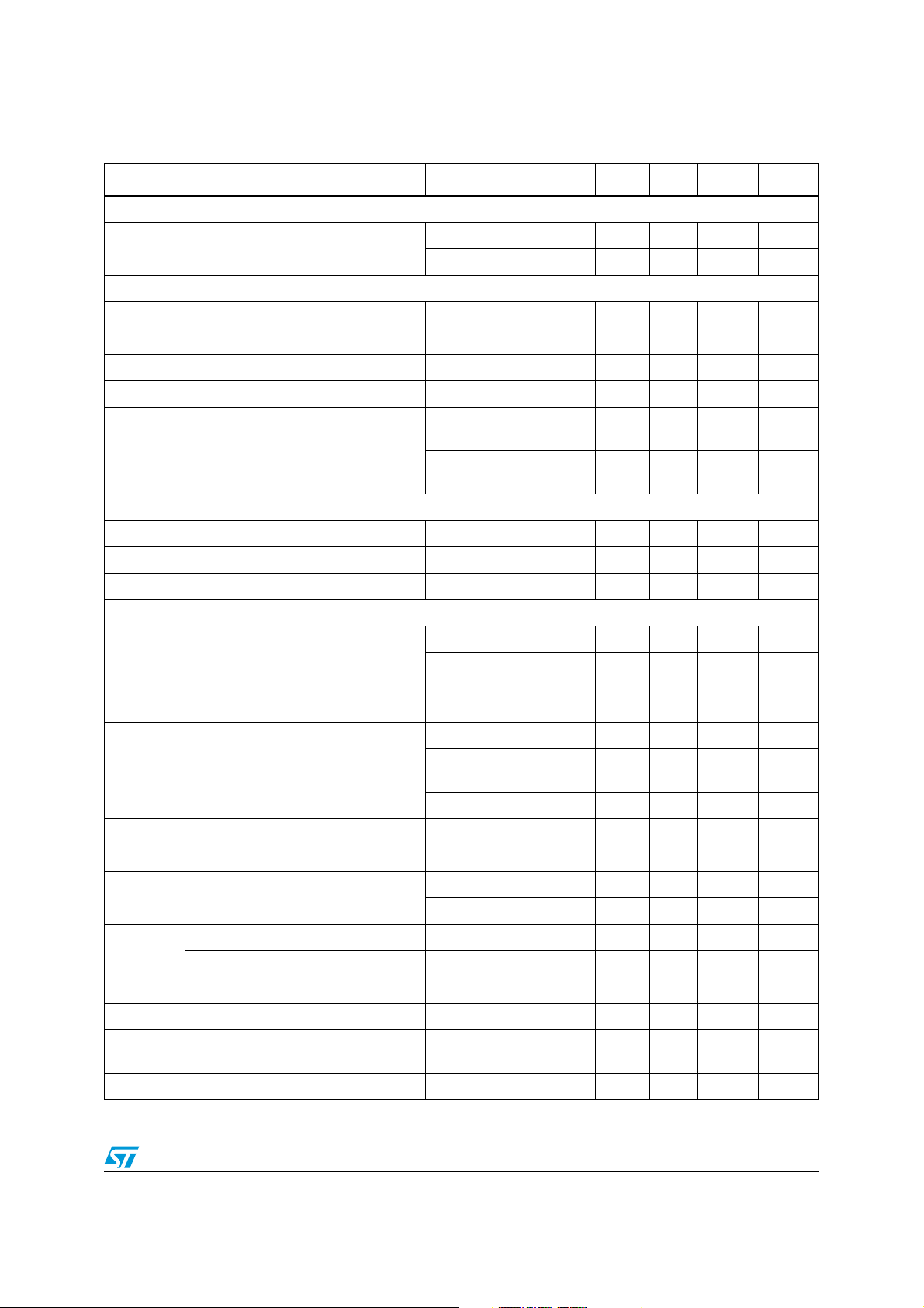
Table 7. Pin diode attenuator driver (dual output current DAC) electrical characteristics
Symbol Parameters
= ABS(FLO-FRF) where FLO is inside the specified LO frequency range.
IF
Conditions Min Typ Max Unit
R Resolution - - 10 - Bit
DNL Differential non linearity - -0.05 - 0.05 LSB
INL Integral non linearity - -0.45 - 0.45 LSB
I
FS
Full Scale current
(1)
-0.28-2.8mA
- Current Mismatch - - - 2 %
-
VR
EXT_DAC
R
EXT_DAC
Icc
static
1. See relationship between IDAC and R
Output voltage compliance
range
-0-3V
Voltage Reference - - 1.19 V
REXT DAC Range - 10 - 100 kΩ
Static current consumption (Iout = 0 mA; pin 1) - 2.5 - mA
in the Circuit Description section (Dual Output Current DAC)
EXT_DAC
16/67 Doc ID 018355 Rev 5
STW82100B Electrical characteristics
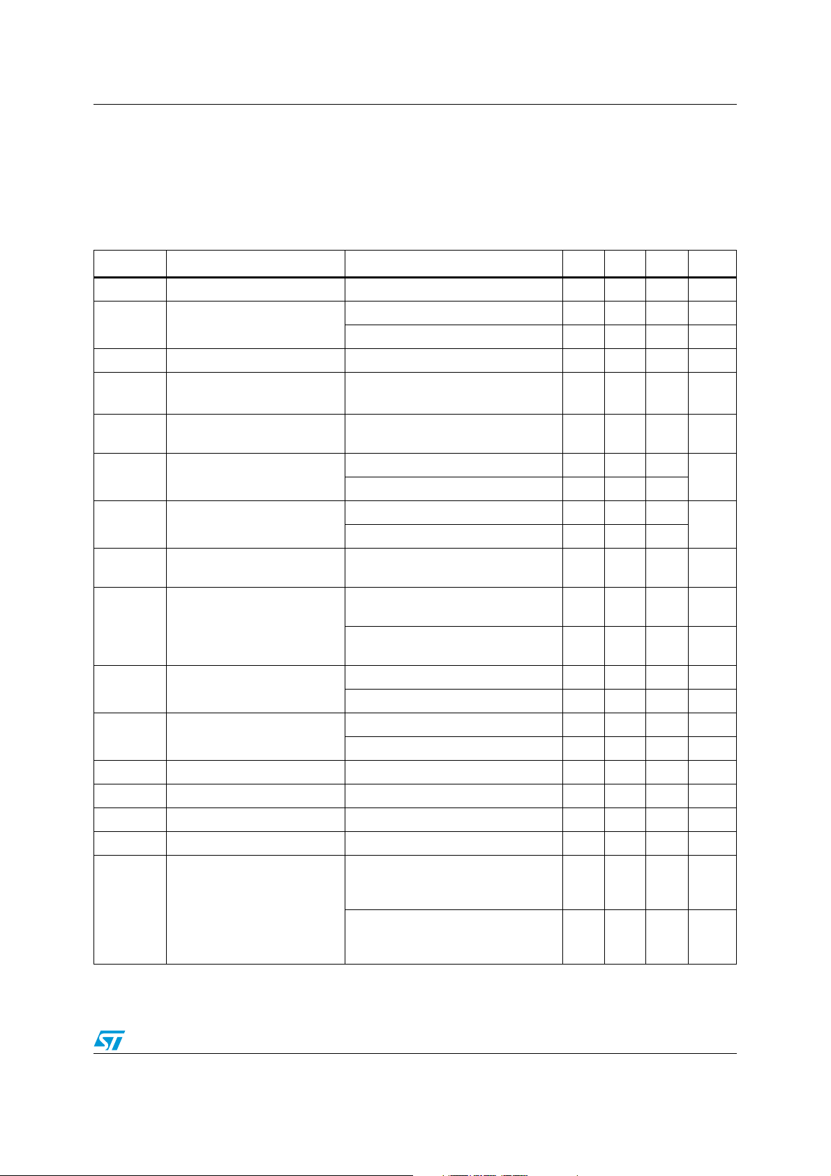
Table 8. Integer-N synthesizer electrical characteristics
Symbol Parameter Conditions Min Typ Max Unit
VCO dividers
Prescaler 16/17 256 - 65551 -
N VCO Divider Ratio (N)
Prescaler 19/20 361 - 77836 -
Reference clock and phase frequency detector
F
ref
Reference input frequency - 10 19.2 200 MHz
- Reference input sensitivity - 0.35 1 1.5 Vpeak
R Reference Divider Ratio - 2 - 1023
F
PFD
F
STEP
PFD input frequency - - - 16 MHz
Frequency step
(1)
Prescaler 16/17
Prescaler 19/20
F
LO
65551
F
LO
77836
/
-
/
-
F
LO
256
F
LO
361
/
Hz
/
Hz
Charge pump
I
V
CP
OCP
ICP sink/source
Output voltage compliance range - 0.4 - Vdd-0.3 V
- Spurious
(3)
(2)
3bit programmable - - 5 mA
---70-dBc
VCOs
Higher frequency range - 100 - MHz/V
K
VCOA
VCOA sensitivity
Intermediate frequency
range
- 85 - MHz/V
Lower frequency range - 70 - MHz/V
Higher frequency range - 75 - MHz/V
K
VCOB
VCOB sensitivity
Intermediate frequency
range
- 65 - MHz/V
Lower frequency range - 55 - MHz/V
ΔT
ΔT
LKA
LKB
VCOA Maximum Temperature
variation for continuous lock
(4)
VCOB Maximum Temperature
variation for continuous lock
(4)
CALTYPE [0] - - 125 °C
CALTYPE [1] - - 125 °C
CALTYPE [0] - - 95 ° C
CALTYPE [1] - - 125 °C
VCO A Pushing - - 8 - MHz/V
VCO B Pushing - - 14 - MHz/V
V
CTRL
VCO control voltage - 0.4 Vdd-0.3 V
- LO Harmonic Spurious - - -20 dBc
I
VCO
IDIV
2
VCO and VCO buffer current
consumption
Amplitude [11] (pin 4) - 35 - mA
DIVIDER by 2 consumption (pin 3) - 20 - mA
Doc ID 018355 Rev 5 17/67
Electrical characteristics STW82100B
Table 8. Integer-N synthesizer electrical characteristics (continued)
Symbol Parameter Conditions Min Typ Max Unit
2 x LO output buffer (test purpose only)
F
P
OUT
OUT
Frequency range - 3.3 - 4.74 GHz
Output level - - 0 - dBm
RL Return Loss Matched to 50ohm - 15 - dB
I
2LOBUF
Current Consumption (pin 15, 16, 17) - 26 - mA
LO output buffer
F
P
OUT
OUT
Frequency range - 1.65 - 2.37 GHz
Output level - - 3 - dBm
RL Return Loss Matched to 50ohm - 14 - dB
I
LOBUF
Current Consumption (pin 15, 16, 17) - 26 - mA
External VCO (LO) buffer
f
INVCO
P
IN
I
EXTBUF
Frequency range - 1.65 - 2.37 GHz
Input level - - 0 - dBm
Current Consumption
External VCO Buffer
(pin 4)
-25 -mA
PLL miscellaneous
Input Buffer, Prescaler,
I
PLL
PLL Current Consumption
Digital Dividers, misc.
-8 -mA
(pin 24)
I
PRE
I
CP
t
LOCK
Prescaler input buffer Current
Consumption
Charge Pump Current Consumption
Lock up time
(5)
(pin 12) - 3 - mA
CPSEL=[111], REXT_CP
= 4.7 kΩ (pin 21)
-4 -mA
25 kHz PLL bandwidth;
within 1ppm of frequency
-150 -µs
error
1. The frequency step is related to the PFD input frequency as follows: F
2. See relationship between ICP and R
3. The level of spurs may change depending on PFD frequency, Charge Pump current, selected channel and PLL loop BW.
4. When setting a specified output frequency, the VCO calibration procedure must be run first in order to select the best
subrange for the VCO covering the desired frequency. Once programmed at the initial temperature T
temperature range (-40 oC to +85 oC), the synthesizer is able to maintain the lock status if the temperature drift (in either
direction) is within the limit specified by ΔT
range.
5. Frequency jump form 1950 to 1800 MHz; it includes the time required by the VCO calibration procedure (7 x F
=17.5 µs with F
=400 kHz))
PFD
in the Circuit Description section (Charge Pump)
EXT_CP
LKA or ΔTLKB
, provided that the final temperature T1 is still inside the nominal
STEP=FPFD
/2)
inside the operating
0
cycles
PFD
18/67 Doc ID 018355 Rev 5
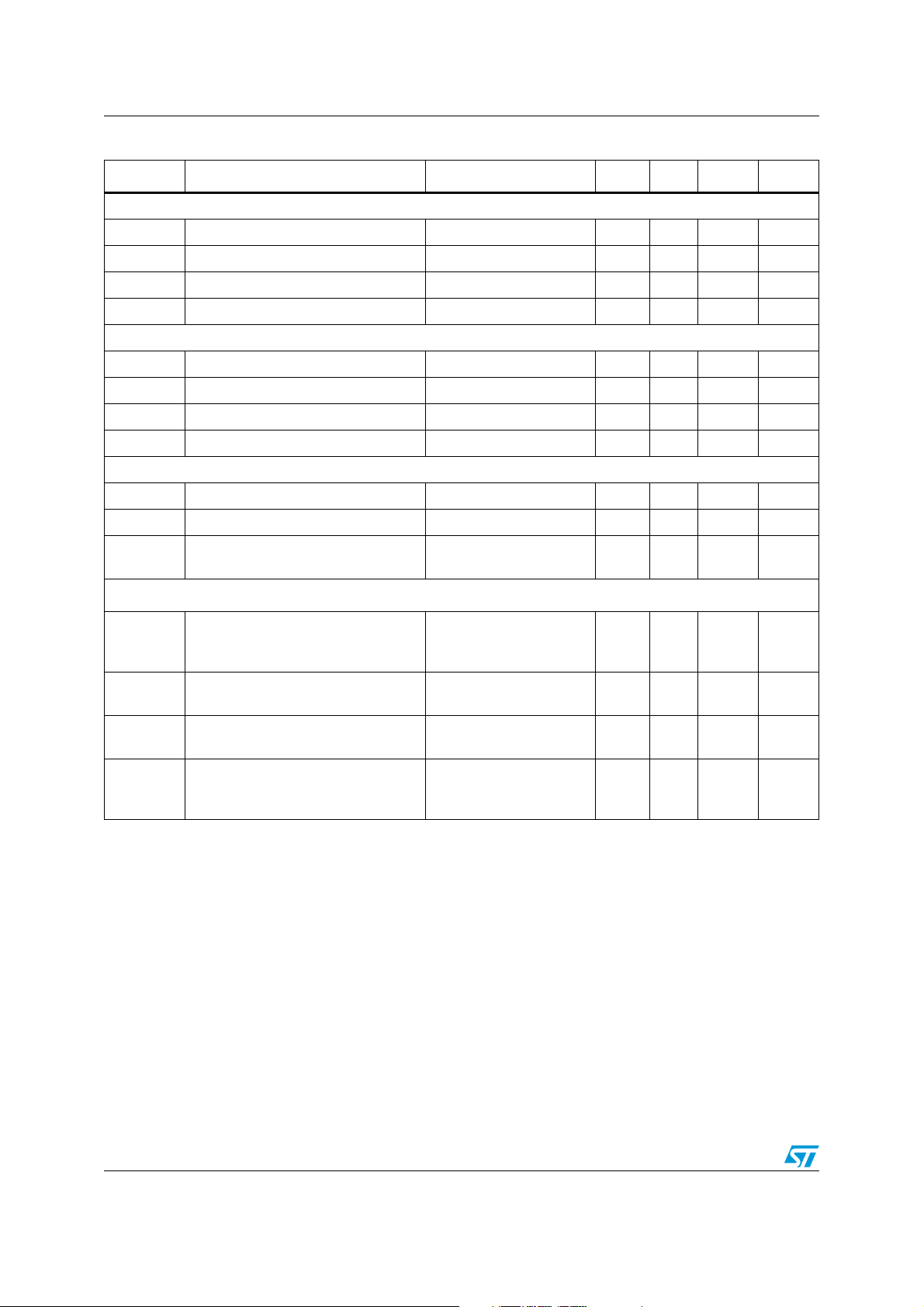
STW82100B Electrical characteristics
Table 9. Phase noise performance
(1)
Parameters Conditions Min. Typ. Max. Unit
In band phase noise floor, closed loop
Normalized In Band Phase Noise
Floor (LO)
In Band Phase Noise Floor (LO) -230+20log(N)+10log(F
(2)
I
=4 mA, PLL BW = 50 kHz
CP
(including reference clock
contribution)
--230-
) dBc/Hz
PFD
dBc/Hz
PLL integrated phase noise
Integrated Phase Noise
(single sided)
100 Hz to 40 MHz
=2.200 GHz, F
F
LO
STEP
=200 kHz,
ICP=3 mA, PLL BW = 25 kHz
--45-dBc
- 0.48 - ° rms
LOA (1650 MHz to 1950 MHz) – open loop
Phase Noise @ 1 kHz - - -69 - dBc/Hz
Phase Noise @ 10 kHz - - -95 - dBc/Hz
Phase Noise @ 100 kHz - - -118 - dBc/Hz
Phase Noise @ 1 MHz - - -139 - dBc/Hz
Phase Noise @ 10 MHz - - -152 - dBc/Hz
Phase Noise Floor @ 40 MHz - - -154 - dBc/Hz
LOB (2050 MHz to 2370 MHz) – open loop
Phase Noise @ 1 kHz - - -62 - dBc/Hz
Phase Noise @ 10 kHz - - -88 - dBc/Hz
Phase Noise @ 100 kHz - - -112 - dBc/Hz
Phase Noise @ 1 MHz - - -134 - dBc/Hz
Phase Noise @ 10 MHz - - -150 - dBc/Hz
Phase Noise Floor @ 40 MHz - - -153 - dBc/Hz
1. Phase Noise SSB. VCO amplitude set to maximum value [11]. All the closed-loop performances are specified using a
Reference Clock signal at 76.8 MHz with phase noise of -144 dBc/Hz @1 kHz offset, -157 dBc/Hz @10 kHz offset and
-168 dBc/Hz of noise floor.
2. Normalized PN = Measured LO PN – 20log(N) – 10log(F
comparison frequency at the PFD input
) where N is the VCO divider ratio (N=B*P+A) and F
PFD
PFD
is the
Doc ID 018355 Rev 5 19/67
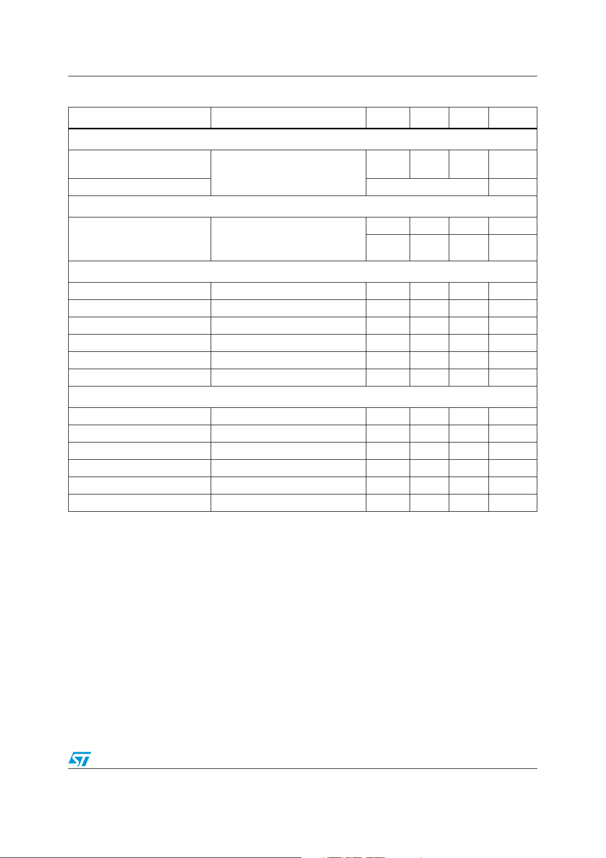
Typical performance characteristics STW82100B
7 Typical performance characteristics
Note: Vsupply digital = 3.3 V, Vsupply analog1 = 3.3 V, Vsupply analog2 = 5 V, F
T
= +25 °C, RF power = 0 dBm, unless otherwise specified.
A
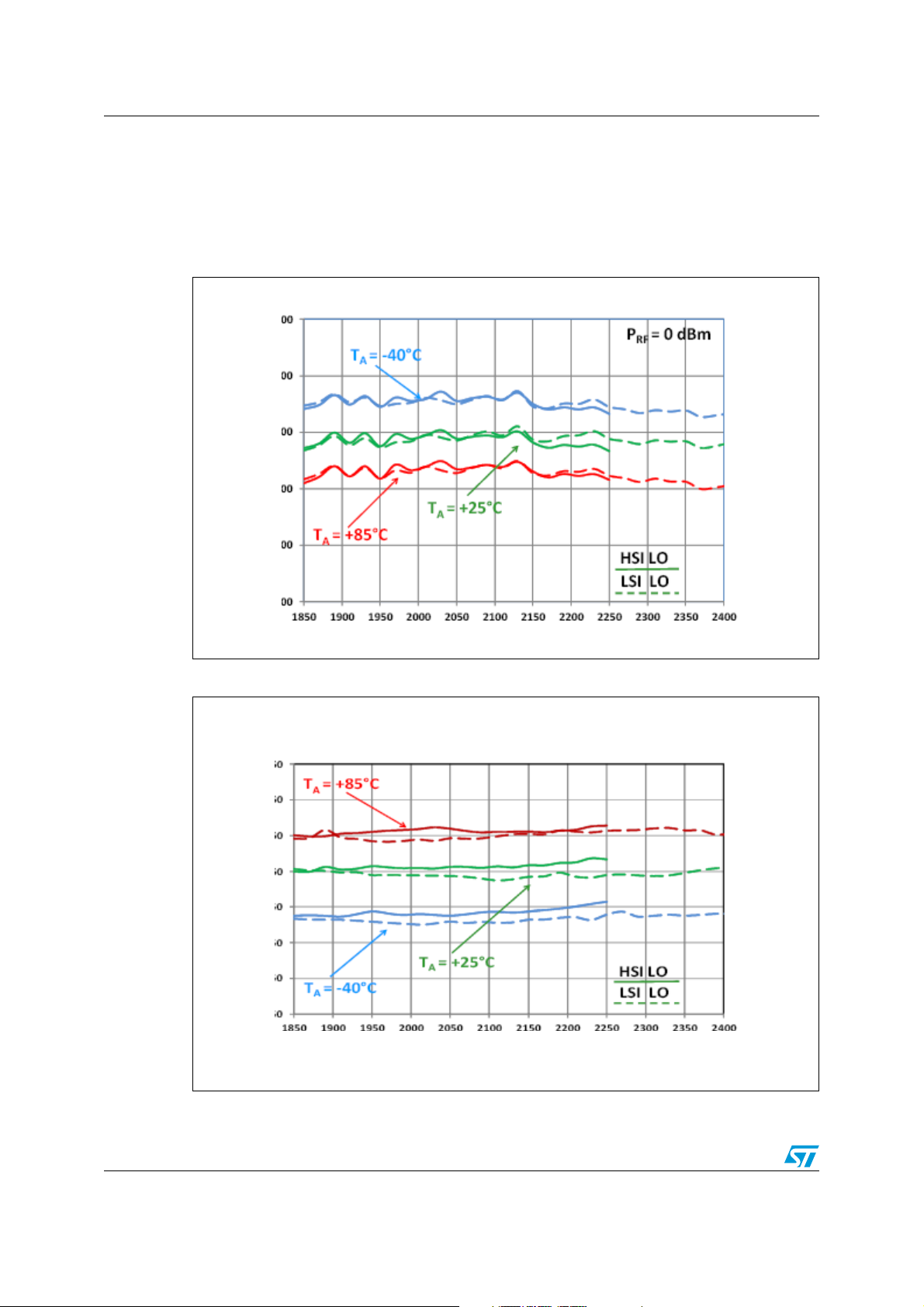
Figure 3. Conversion gain against RF frequency
Conversion gain (dB)
RF frequency (MHz)
= 150 MHz,
IF
Figure 4. Noise figure against RF frequency
Noise figure (dB)
RF frequency (MHz)
20/67 Doc ID 018355 Rev 5
STW82100B Typical performance characteristics
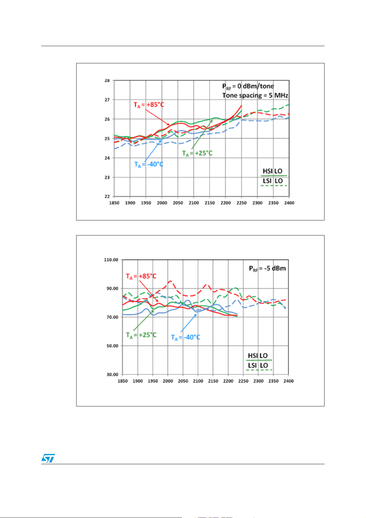
Figure 5. IIP3 against RF frequency
IIP3 (dBm)
RF frequency (MHz)
Figure 6. 2RF-2LO response against RF frequency
2RF-2LO response (dB)
RF frequency (MHz)
Doc ID 018355 Rev 5 21/67
 Loading...