

查询STW4141供应商
for Digital Base Band and Multimedia Processor Supply
STw4141
Single Coil Dual Output Step Down DC/DC Converter
PRELIMINARY DATA
Features
■ Single coil dual output switc hi ng co nve r ter for
digital core supply & digital I/Os supply
– Digital I/O supply:V
– CPU CORE supply:V
■ Wide range of fixed output voltage
configurations availabl e
■ High efficiency synchronous step down
converter with up to 92 % for the entire device
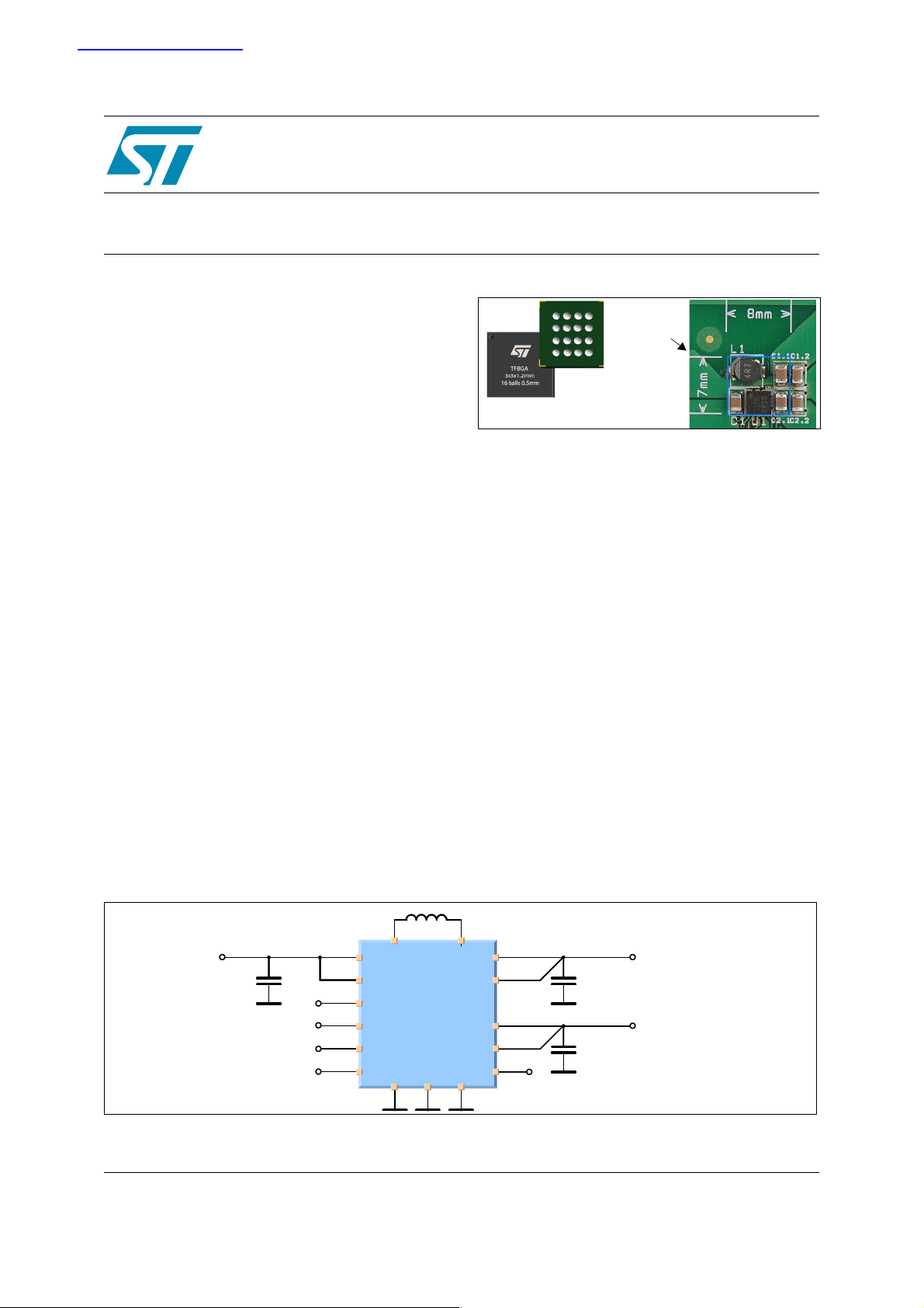
■ Size and cost optimized application board
(7x8 mm, height 1.2mm) three capacitors and
only one inductor necessary for both outputs
■ 2.7 V to 5.5 V battery input range
■ ±100mV output voltage accuracy full range in
PWM (Including Line and Load Transients)
■ 900 kHz fixed frequency PWM oper ation
■ PFM mode operation at light load current
■ PWM/PFM switch can be done automatically or
forced by setting external pin s (AUTO and
MODE/SYNC)
■ MODE/SYNC input pin for external clock
synchronization from 600 kHz to 1.5 MHz
■ VSEL input pin for V
■ Ultra low shutdown current (Iq<1 µA)
■ Short circuit and thermal shutdown protections
OUT2/VOUT2(red.)
OUT1
OUT2
@ 200 mA
@ 400 mA
selection
Solution size
7 x 8 mm
TFBGA 3x3mm
16 bumps 0.5 mm pitch
Applications
■ Mobile phones
■ PDAs and hand held terminals
■ Portable media players
■ Digital still camera
■ WLAN and Bluetooth applications
Description
The STw4141 is a single coil dual output
synchronous step down DC/DC converter that
requires only four standard external components.
It operates at a fixed 900 kHz switching frequency
in PWM mode. The device can operate in PFM
mode to maintain high efficiency over the full
range of output currents.
The STw4141 application requires a very small
PCB area and offers a very efficient, accurate,
space and cost saving solution to fulfill the
requirements of digital baseband or multimedia
processor supply (CORE & I/O).
Application Test Circuit
L 4.7 µH
L 4.7 µH
VLX1 VLX2
VLX1 VLX2
=2.7V to 5.5V
=2.7V to 5.5V
V
V
IN
IN
C
C
IN
IN
10 µF
10 µF
6.3 V
6.3 V
MODE/SYNC
MODE/SYNC
PVDD
PVDD
VDD
VDD
EN
EN
AUTO
AUTO
VSEL
VSEL
A2 A3
A2 A3
B1
B1
D3
D3
D4
D4
STw4141
STw4141
C2
C2
C3
C3
C1
C1
A1B3C4
A1B3C4
PGND
PGND
GND
GND
A4
A4
D1
D1
B4
B4
D2
D2
B2
B2
T_MODE
T_MODE
VOUT1
VOUT1
FB1
FB1
VOUT2
VOUT2
FB2
FB2
STATE
STATE
C
C
OUT1
OUT1
22 µF
22 µF
6.3 V
6.3 V
C
C
OUT2
OUT2
22 µF
22 µF
6.3 V
6.3 V
December 2005 1/27
This is preliminary information on a new product now in development or undergoing evaluation. Details are subject to
change without notice.
V
V
OUT1
OUT1
V
V
OUT2
OUT2
=1.8V
=1.8V
=1.0V/1.2V
=1.0V/1.2V
Rev 1
www.st.com
2
STw4141
Order Codes
Table 1. STw4141 ordering information
(1)
V
OUT2reduced
(CORE)
Supplied as
Part number Package type
Package
marking
Output voltage options
(2)
V
OUT1
(I/O)
(CORE)
V
OUT2
STw41411
STA1 1.8 V 1.2 V 1.0 V Tray
STw41411/T STA1 1.8 V 1.2 V 1.0 V Tapes/Reels
STw41412 STA2 1.8 V 1.3 V 1.0 V Tray
STw41412/T STA2 1.8 V 1.3 V 1.0 V Tapes/Reels
STw41413 STA3 1.5 V 1.3 V 1.0 V Tray
STw41413/T STA3 1.5 V 1.3 V 1.0 V Tapes/Reels
TFBGA
3x3x1.2
STw41414 STA4 1.8 V 1.5 V 1.3 V Tray
16 balls
STw41414/T STA4 1.8 V 1.5 V 1.3 V Tapes/Reels
STw41415 STA5 1.8 V 1.35 V 1.0 V Tray
STw41415/T STA5 1.8 V 1.35 V 1.0 V Tapes/Reels
STw41416 STA6 1.8 V 1.25 V 1.0 V Tray
STw41416/T STA6 1.8 V 1.25 V 1.0 V Tapes/Reels
1. The output configuration which will be introduced in production will be only those related to customer design-in.
2. THIS CONDITION MUST BE ALWAYS VALID.
VOUT1 VOUT2≥
2/27

STw4141
Contents
1 STw4141 Pinout . . . . . . . . . . . . . . . . . . . . . . . . . . . . . . . . . . . . . . . . . . . . . . 5
2 Electrical Characteristics . . . . . . . . . . . . . . . . . . . . . . . . . . . . . . . . . . . . . . . 7
2.1 Absolute maximum ratings . . . . . . . . . . . . . . . . . . . . . . . . . . . . . . . . . . . . . . . 7
2.2 Thermal data . . . . . . . . . . . . . . . . . . . . . . . . . . . . . . . . . . . . . . . . . . . . . . . . . . 7
2.3 DC electrical characteristics . . . . . . . . . . . . . . . . . . . . . . . . . . . . . . . . . . . . . . 8
2.4 Dynamic electrical characteristics . . . . . . . . . . . . . . . . . . . . . . . . . . . . . . . . . . 9
2.5 Soft start . . . . . . . . . . . . . . . . . . . . . . . . . . . . . . . . . . . . . . . . . . . . . . . . . . . . 10
2.6 Settling time of VOUT2 . . . . . . . . . . . . . . . . . . . . . . . . . . . . . . . . . . . . . . . . . 10
2.7 Line transients . . . . . . . . . . . . . . . . . . . . . . . . . . . . . . . . . . . . . . . . . . . . . . . . 11
2.8 Load transients in AUTO mode . . . . . . . . . . . . . . . . . . . . . . . . . . . . . . . . . . . 11
2.9 Load transients in PWM mode . . . . . . . . . . . . . . . . . . . . . . . . . . . . . . . . . . . 12
2.10 Switching between PFM and PWM in FORCED MODE . . . . . . . . . . . . . . . . 13
2.11 Efficiency in PWM . . . . . . . . . . . . . . . . . . . . . . . . . . . . . . . . . . . . . . . . . . . . . 14
2.12 Efficiency in AUTO . . . . . . . . . . . . . . . . . . . . . . . . . . . . . . . . . . . . . . . . . . . . 15
2.13 Output voltages versus output currents in PWM and PFM . . . . . . . . . . . . . . 16
3 Functional Description . . . . . . . . . . . . . . . . . . . . . . . . . . . . . . . . . . . . . . . . 17
3.1 Introduction . . . . . . . . . . . . . . . . . . . . . . . . . . . . . . . . . . . . . . . . . . . . . . . . . . 17
3.2 PWM and PFM mode operation . . . . . . . . . . . . . . . . . . . . . . . . . . . . . . . . . . 17
3.3 Current limiter . . . . . . . . . . . . . . . . . . . . . . . . . . . . . . . . . . . . . . . . . . . . . . . . 17
3.4 Short circuit protection . . . . . . . . . . . . . . . . . . . . . . . . . . . . . . . . . . . . . . . . . 17
3.5 Thermal shutdown protection . . . . . . . . . . . . . . . . . . . . . . . . . . . . . . . . . . . . 18
4 Application information . . . . . . . . . . . . . . . . . . . . . . . . . . . . . . . . . . . . . . . 18
4.1 User mode details . . . . . . . . . . . . . . . . . . . . . . . . . . . . . . . . . . . . . . . . . . . . . 18
4.2 Aut omatic PWM/PFM mode . . . . . . . . . . . . . . . . . . . . . . . . . . . . . . . . . . . . . 19
4.3 User selected PWM/PFM mode . . . . . . . . . . . . . . . . . . . . . . . . . . . . . . . . . . 19
4.4 External clock synchronization . . . . . . . . . . . . . . . . . . . . . . . . . . . . . . . . . . . 20
4.5 Checking Transient response versus external components . . . . . . . . . . . . . 20
4.6 Bill of Material . . . . . . . . . . . . . . . . . . . . . . . . . . . . . . . . . . . . . . . . . . . . . . . . 20
4.6.1 Inductor selection . . . . . . . . . . . . . . . . . . . . . . . . . . . . . . . . . . . . . . . . . . . . . 20
3/27

STw4141
4.6.2 Input capacitor (CIN selection) . . . . . . . . . . . . . . . . . . . . . . . . . . . . . . . . . . . 21
4.6.3 Output capacitors (COUT selection) . . . . . . . . . . . . . . . . . . . . . . . . . . . . . . . 21
4.6.4 Capacitors selection . . . . . . . . . . . . . . . . . . . . . . . . . . . . . . . . . . . . . . . . . . . 21
4.7 PCB layout considerations . . . . . . . . . . . . . . . . . . . . . . . . . . . . . . . . . . . . . . 21
4.7.1 PCB layout . . . . . . . . . . . . . . . . . . . . . . . . . . . . . . . . . . . . . . . . . . . . . . . . . . . 22
4.7.2 TFBGA16 internal bumps access . . . . . . . . . . . . . . . . . . . . . . . . . . . . . . . . . 23
5 Package Outline and Mechanical Data . . . . . . . . . . . . . . . . . . . . . . . . . . . 24
6 Revision history . . . . . . . . . . . . . . . . . . . . . . . . . . . . . . . . . . . . . . . . . . . . . . 26
4/27
STw4141 1 STw4141 Pinout
1 2 3
4
/
1 2 3
4
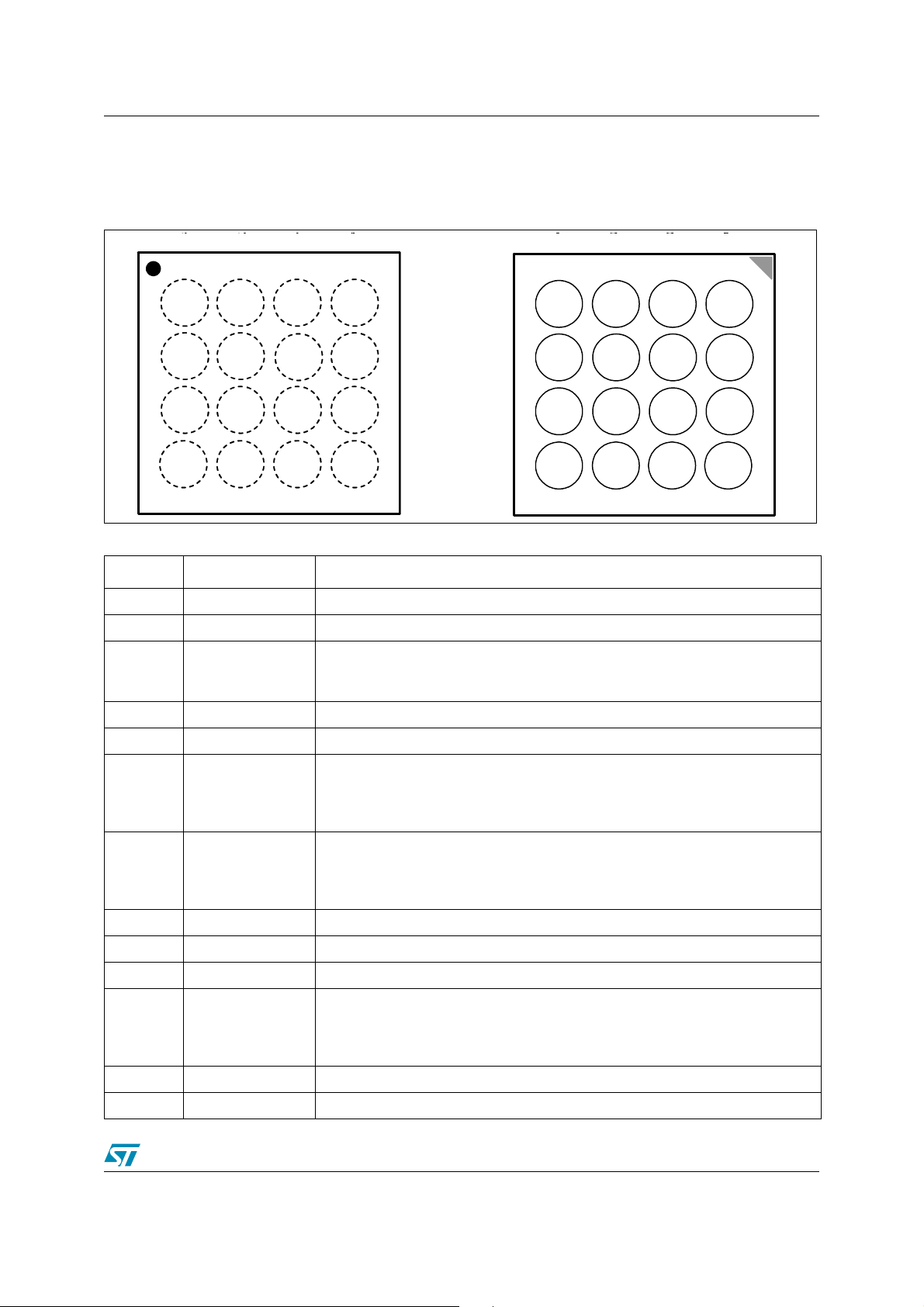
1 STw4141 Pinout
Figure 1. Pin assignment in TFBGA 3x3 mm - 16 bumps 0.5 mm pitch
12 34
4321
A
B
C
D
PGND
PVDD
MODE/
SYNC
FB1
VLX1
STATE
AUTO
FB2
VLX2
T_MODE
VSEL
VDD
VOUT1
VOUT2
GND
EN
Top v i ew
Table 2. STw4141 pin description
Pin Symbol Description
A1 PGND Power ground
B1 PVDD Power supply voltage
MODE/SYNC = High to forced PWM mode
C1 MODE/SYNC
D1 FB1 Feedback 1
A2 VLX1 External inductor connection pin 1
B2 STATE
MODE/SYNC = Low to forced PFM mode
MODE/SYNC = 600 kHz - 1.5 MHz external clock synchronization in PWM
Output STATE pin allow the user to monitor operation mode of the product
STATE = High - PFM mode
STATE = Low - PWM mode
If not used must be left unconnected.
VOUT1
VOUT2
GND
EN
VLX2
T_MODE
VSEL
VDD
Bottom view
VLX1
STATE
AUTO
FB2
PGND
PVDD
MODE
SYNC
FB1
A
A
B
B
C
C
D
D
PWM/PFM automatic switch control pin
C2 AUTO
AUTO = High - PWM/PFM mode automatic switch ENABLED
AUTO = Low - PWM/PFM mode automatic switch DISABLED
PWM/PFM mode controlled by MODE/SYNC pin)
D2 FB2 Feedback 2
A3 VLX2 External inductor connection pin 2
B3 T_MODE Input signal for test mode selection. This pin must be connected to GND.
Voltage selection input
C3 VSEL
VSEL = High - VOUT1 = 1.8V, VOUT2 = 1.2V (valid for STA1)
VSEL = Low - VOUT1 = 1.8V, VOUT2 = 1.0V (valid for STA1)
(For other voltage options see
Table 1: STw4141 ordering information
)
D3 VDD Signal supply voltage
A4 VOUT1 Output voltage 1
5/27
1 STw4141 Pinout STw4141
Table 2. STw4141 pin description
Pin Symbol Description
B4 VOUT2 Output voltage 2
C4 GND Signal ground
Enable Input:
D4 EN
EN = Low - Device in shutdown mode,
EN = High - Enable device
This pin must be connected either to VDD or GND.
PGND pin
This is the ground pin related to power sign al. This pin should be connected to the board ground
plane by short and wide track or multiply vias to reduce impedance and EMI.
GND pins This is the ground pin related to analog signal.
PVDD pin
This pin is designed to provide power to the device. This path leads high currents. It should be
wide and short to minimize track impedance to reduce losses and EMI.
VDD pin
This pin is designed to provide signal supply voltage to the device. There is no specific
requirement for its related track design.
VLX1/VLX2 pins
External coil is connected on those pins. It should be placed as closed as possible to the device
in order minimize resistances which cause looses. These paths lead high currents.
VOUT1 pin3
It is the first output voltage of this device. This path leads high currents. It should be wide and
short to minimize track impedance to reduce losses and EMI.
VOUT2 pin
It is the second output v olta ge of t his d e vic e. This p ath le ads h igh c urrents . It shou ld be wide and
short to minimize track impedance to reduce losses and EMI.
FB1 pin Intended to measure VOUT1 voltage in order to ensure the regulation of this output.
FB2 pin Intended to measure VOUT2 voltage in order to ensure the regulation of this output.
ENABLE pin
This is the enable pin of the device. Pulling this pin to ground, forces the device into shutdown
mode. Pulling this pin to VDD enables the device. This pin must be terminated.
MODE/SYNC pin
The MODE/SYNC pin is a multipurpose pin which provides mode selection and frequency
synchronization.
The devic e c an al so be s yn chr onized to an external cl ock signal from 600 kHz to 1.5 MHz by the
MODE/SYNC pin. During synchronization, the mode is forced to PWM mode and the top switch
turn-on is synchronized to the rising edge of the external clock.
AUTO pin
This pin allows th e de vice to au tomatica lly s witch from PWM to PFM mo de f ollowi ng load on b oth
2 outputs.
STATE pin This output pin informs user in which state the device is working: PWM or PFM mode.
VSEL pin
This pin is used to reduce V
(CORE) output voltage in order to r edu ce the proc essor power
OUT2
consumption when entering into sleep mode.
6/27
STw4141 2 Electrical Characteristics
2 Electrical Characteristics
2.1 Absolute maximum ratings
Absolute maximum ratings are those values beyond which damage to the device may occur.
Functional operation under these conditions is not implied. All voltages are referenced to GND.
Table 3. Absolute maximum ratings
Symbol Parameter Value Unit
PV
DD
V
DD
V
EN
V
SEL
V
MODE/SYNC
V
AUTO
V
T_MODE
V
STATE
,FB
V
OUT1
V
OUT2, FB2
VLX
1
VLX
2
T
A
T
J
T
STG
Power Supply Voltage -0.3 to 6 V
Signal Supply Voltage -0.3 to 6 V
Enable Input
V oltage Selection
Operating Mode Selection/Synchronization Input
PWM/PFM automatic switch selection
Test mode select ion
Operating mode information
Output Voltage 1, Feedback 1 -0.3 to 3.3 V
1
-0.3 to V
-0.3 to V
-0.3 to V
-0.3 to V
-0.3 to V
-0.3 to V
DD
DD
DD
DD
DD
OUT1
Output Voltage 2, Feedback 2 -0.3 to 3.3 V
External Inductor Connection Pin 1
-0.3 to V
DD
External Inductor Connection Pin 2 -0.3 to 3.3 V
Operating Temperature Range -40 to 85 °C
Maximum Operating Junction Temperature 150 °C
Storage Temperature Range -65 to 150 °C
V
V
V
V
V
V
V
2.2 Thermal data
Table 4. Thermal data
Symbol Parameter Value Unit
R
thJA
Thermal Resistance Junction-Ambient
TFBGA 3x3 mm – 16 bumps - 0.5 mm pitch
150 °C/W
7/27
2 Electrical Characteristics STw4141
2.3 DC electrical characteristics
Characteristics measured over recommended operating conditions unless otherwise is noted.
All typical values are referred to T
Table 5. DC electrical characteristics
Symbol Parameter Test Conditions Min. Typ Max. Unit
PVDD Power supply voltage 2.7 5.5 V
I
LIM
V
OUT1
V
OUT2
Peak current limit 1.6 A
(1)
Output voltage 1
Output voltage 2
Output voltage 2
(2)
(2)
(2)
VSEL = VDD,
MODE/SYNC = VDD
VSEL = GND,
MODE/SYNC = VDD
= 25°C, PVDD = 3.6V, VDD = 3.6V.
A
-3 +3 %
-3 +3 %
-3 +3 %
I
OUT1
I
OUT2
Output current 1 200 mA
Output current 2 400 mA
Quiescent Current
(PWM)
I
q
Quiescent Current
(PFM)
Shutdown Current
Enable functions
H
V
EN
V
EN
Enable Threshold High 0.9 V
L
Enable Threshold Low 0.4 V
Mode/sync functions
H
L
MODE/SYNC
Threshold High
MODE/SYNC
Threshold Low
V
M/S
V
M/S
I
OUT1
= 0 mA, I
OUT2
= 0 mA
EN = VDD, VSEL = VDD
MODE/SYNC = VDD,
AUTO = GND
I
OUT1
= 0 mA, I
OUT2
= 0 mA
EN = VDD, VSEL = VDD
MODE/SYNC = GND,
AUTO = GND
EN = GND,
VSEL = GND
MODE/SYNC = GND,
AUTO = GND
600 µA
90 µA
15µA
0.9 V
0.4 V
VSEL functions
Voltage Selection
H
V
V
SEL
SEL
Threshold High
Voltage Selection
L
Threshold Low
8/27
0.9 V
0.4 V
STw4141 2 Electrical Characteristics
Table 5. DC electrical characteristics
Symbol Parameter Test Conditions Min. Typ Max. Unit
Auto functions
Voltage Selection
H
V
AUTO
V
AUTO
Threshold High
Voltage Selection
L
Threshold Low
State functions
Voltage Selection
H
V
STATE
V
STATE
1. . This condition must always be valid.
VOUT1 VOUT2≥
2. Output voltage accuracy excludes line and load transients
Threshold High
Voltage Selection
L
Threshold Low
R
R
Lmax
Lmax
= 100k, C
= 100k, C
Lmax
Lmax
= 10pF 0.7V
= 10pF 0.3 V
0.9 V
0.4 V
OUT1
OUT1
V
V
2.4 Dynamic electrical characteristics
Characteristics measured over recommended operating conditions unless otherwise is noted.
All typical values are referred to T
= 25°C, PVDD = 3.6V, VDD = 3.6V.
A
Table 6. Dynamic electrical characteristics
Symbol Parameter Test Conditions Min. Typ Max. Unit
f
SW
f
SYNC
Ts Settling time (soft start) 400 µs
TS2
Switching frequency 900 kHz
Sync mode frequency 600 1500 kHz
Settling time
V
(reduced)/V
OUT2
VSEL change from GND to VDD 80 µs
OUT2
9/27

2 Electrical Characteristics STw4141
2.5 Soft start
To avoid spikes on battery during STw4141 start-up sequence, a smooth start-up is
implemented. Reference voltage grows up less than 600 µs until it achieves is final target.
Therefore, STw4141 start up is smooth and secure for the overall mobile phone.
Figure 2. Smooth start-up sequence V
V
=1.2V@400mA
OUT2
2.6 Settling time of V
OUT2
= 3.6V, V
IN
= 1.8V@ 200mA,
OUT1
Figure 3. Settling time of V
10/27
OUT2, IOUT1
= 200mA, I
OUT2
= 400mA

STw4141 2 Electrical Characteristics
2.7 Line transients
Figure 4. Line transient, V
= 1.8V @ 100mA, V
OUT1
2.8 Load transients in AUTO mode
Figure 5. Load transient in AUTO mode VIN = 3.6V, V
= 1.2V @ 100mA
OUT2
= 1.8V, V
OUT1
OUT2
= 1.2V
11/27

2 Electrical Characteristics STw4141
2.9 Load transients in PWM mode
Figure 6: Load transient in PWM mode, I
Load transient related to in-phase switching
VIN = 3.6V, V
Load transient output 2 leading output 1
= 3.6V, V
V
IN
OUT1
OUT1
= 1.8V, V
= 1.8V, V
OUT2
OUT2
= 1.2V
= 1.2V
= 1mA to 200mA, I
OUT1
= 1mA to 400mA
OUT2
Load transient output 1 leading output 2
= 3.6V, V
V
IN
OUT1
= 1.8V, V
OUT2
Load transient related to anti-phase switching
VIN = 3.6V, V
OUT1
= 1.8V, V
OUT2
= 1.2V
= 1.2V
12/27

STw4141 2 Electrical Characteristics
2.10 Switching between PFM and PWM in FORCED MODE
Figure 7. Switching between PFM to PWM operation modes VIN = 3.6V, I
= 10mA
I
OUT2
Figure 8. Switching between PWM to PFM operation modes V
I
= 10mA
OUT2
= 3.6V, I
IN
OUT1
OUT1
= 10mA,
= 10mA,
13/27

2 Electrical Characteristics STw4141
2.11 Efficiency in PWM
The efficiency of a switching regulator is equal to the total output power divided by the input.
STw4141 has high efficiency up to 92% (for the 2 outputs). Efficiency curve is flat over the
output current range.
Figure 9. Switching regulator efficiency in PWM mode
Efficiency in PWM mode @ VIN=2.7V, TA= 25°C
Efficiency in PWM mode @ VIN=3.6V, TA= 25°C
200
180
160
140
120
I
(mA)
OUT1
Efficiency vs I
60
50
40
30
20
10
0
100
80
60
40
20
1
1
100
90
80
70
60
50
40
EFFICIENCY (%)
30
20
10
0
OUT1@IOUT2
V
= 2.7V
IN
V
= 1.8V
OUT1
V
= 1.2V
OUT2
1 10 100 1000
200
160
120
80
40
PWM mode, TA=25°C
I
(mA)
OUT1
400
360
320
280
240
(mA)
I
OUT2
100
90
80
70
Efficiency (%)
90-100
80-90
70-80
60-70
50-60
40-50
30-40
20-30
10-20
0-10
I
= 0 mA
OUT2
I
= 200 mA
OUT2
I
= 400 mA
OUT2
200
180
160
140
120
I
(mA)
OUT1
Efficiency vs I
EFFICIENCY (%)
100
90
80
70
60
50
40
30
20
10
100
80
60
40
20
1
1
100
90
80
70
60
50
40
30
20
10
0
OUT1@IOUT2
V
= 3.6V
IN
V
= 1.8V
OUT1
V
= 1.2V
OUT2
1 10 100 1000
200
160
120
80
40
PWM mode, TA=25°C
I
(mA)
OUT1
0
400
360
320
280
240
I
(mA)
OUT2
I
OUT2
I
OUT2
I
OUT2
Effici ency (%)
90-100
80-90
70-80
60-70
50-60
40-50
30-40
20-30
10-20
0-10
= 0 mA
= 200 mA
= 400 mA
Efficiency vs I
100
V
90
80
70
V
60
V
50
40
EFFICIENCY (%)
30
20
10
0
1 10 100 1000
IN
OUT1
OUT2
= 2.7V
= 1.8V
= 1.2V
OUT2@IOUT1
, PWM mode, TA=25°C
I
(mA)
OUT2
I
= 0 mA
OUT1
I
= 100 mA
OUT1
I
= 200 mA
OUT1
14/27
Efficiency vs I
100
90
80
70
60
50
40
EFFICIENCY (%)
30
20
10
0
1 10 100 1000
V
IN
V
OUT1
V
OUT2
= 3.6V
= 1.8V
= 1.2V
OUT2@IOUT1
, PWM mode, TA=25°C
I
(mA)
OUT2
I
= 0 mA
OUT1
I
= 100 mA
OUT1
I
= 200 mA
OUT1

STw4141 2 Electrical Characteristics
)
)
)
2.12 Efficiency in AUTO
The efficiency of a switching regulator is equal to the total output power divided by the input.
STw4141 has high efficiency up to 92% (both outputs) and always higher than 70% for output
currents higher than 1mA.
Figure 10. Switching regulator efficiency in auto mode
Efficiency VS output currents I
180
150
120
90
I
OUT1
60
(mA)
30
1
Efficiency VS I
100
90
80
70
60
50
40
EFFICIENCY (%)
30
20
10
0
1 10 100 1000
Efficiency VS I
100
90
80
70
60
50
40
EFFICIENCY (%)
30
20
10
0
1 10 100 1000
V
IN
V
OUT1
V
OUT2
V
IN
V
OUT1
V
OUT2
= 2.7V
= 2.7V
= 1.8V
= 1.2V
= 1.8V
= 1.2V
OUT1@IOUT2
OUT2@IOUT1
OUT1
40
80
and I
120
, VIN = 2.7V, AUTO mode
OUT2
320
280
240
200
160
I
(mA)
OUT2
, AUTO mode, TA = 25°C
I
(mA
, AUTO mode, TA = 25°C
I
(mA)
OUT2
Efficiency VS output currents I
100
90
80
70
60
50
Efficiency (%
40
90-100
80-90
30
70-80
20
60-70
50-60
10
40-50
0
30-40
20-30
400
10-20
360
0-10
200
160
120
80
(mA)
I
OUT1
40
1
Efficiency VS IOUT1@I
100
V
= 3.6V
I
= 0 mA
OUT2
I
= 200 mA
OUT2
I
= 400 mA
OUT2
IN
90
80
70
V
= 1.8V
OUT1
V
= 1.2V
60
OUT2
50
40
EFFICIENCY (%)
30
20
10
0
1 10 100 1000
Efficiency VS I
100
V
= 3.6V
I
= 0 mA
OUT1
I
= 100 mA
OUT1
I
= 200 mA
OUT1
IN
90
80
70
60
V
= 1.8V
OUT1
V
= 1.2V
OUT2
50
40
EFFICIENCY (%)
30
20
10
0
1101001000
and I
OUT1
160
120
80
0
OUT2
I
OUT2@IOUT1
I
OUT2
, VIN = 3.6V, AUTO mode
OUT2
100
90
80
70
60
50
Efficiency (%)
40
30
20
10
0
400
360
320
280
240
200
I
(mA)
OUT2
, AUTO mode, TA = 25°C
I
= 0 mA
OUT2
I
= 200 mA
OUT2
I
= 400 mA
OUT2
(mA
, AUTO mode, TA = 25°C
I
= 0 mA
OUT1
I
= 100 mA
OUT1
I
= 200 mA
OUT1
(mA)
90-100
80-90
70-80
60-70
50-60
40-50
30-40
20-30
10-20
0-10
15/27

2 Electrical Characteristics STw4141
2.13 Output voltages versus output currents in PWM and PFM
Figure 11. Output voltages versus output currents in PWM and PFM
V
VS I
OUT1
1.830
V
= 3.6V
IN
1.820
1.810
(V)
1.800
OUT1
V
1.790
OUT1
@ I
- PWM mode
OUT1
I
I
I
OUT2
OUT2
OUT2
= 0 mA
= 200 mA
= 400 mA
V
VS I
OUT2
1.230
V
= 3.6V
IN
1.220
1.210
(V)
1.200
OUT2
V
1.190
OUT2
@ I
- PWM mode
OUT1
I
I
I
OUT1
OUT1
OUT1
= 0 mA
= 100 mA
= 200 mA
1.780
1.770
1 10 100 1000
V
OUT1
1.830
V
= 3.6V
IN
1.820
1.810
(V)
1.800
OUT1
V
1.790
1.780
1.770
110100
VS I
I
OUT1
I
OUT1
OUT1
(mA)
@ I
(mA)
- PFM mode
OUT2
I
= 0 mA
OUT2
I
= 20 mA
OUT2
I
= 40 mA
OUT2
1.180
1.170
1 10 100 1000
V
OUT2
1.230
V
= 3.6V
IN
1.220
1.210
(V)
1.200
OUT2
V
1.190
1.180
1.170
110100
VS I
OUT2
I
(mA)
OUT2
@ I
- PFM mode
OUT1
I
= 0 mA
OUT1
I
= 10 mA
OUT1
I
= 20 mA
OUT1
I
(mA)
OUT2
16/27

STw4141 3 Functional Description
3 Functional Description
3.1 Introduction
The STw4141 is an easy to use, single coil dual outputs step down DC/DC converter optimized
to supply low-voltage to CPUs or DSPs in cell phones and other miniature devices powered by
single cell lithium-ion or 3 cell NiMH/NiCd batteries. It provides two different output voltages
with high efficiency operation in a wide range of output currents. The device offers high DC
voltage regulation accuracy and load transient response to satisfy demanding processor core
supply. The converter is based on voltage mode buck architecture using PWM and PFM
operation modes.
At light load currents, the device can operate in PFM mode to maintain high efficiency over the
entire load current range. Switching between PWM and PFM modes can be done automatically
or can be forced by external pins (AUTO and MODE/SYNC). Externally synchronized or fixed
frequency (internal oscillator) PWM mode offers full output current capability while minimizing
interference to sensitive RF and data acquisition circuits.
3.2 PWM and PFM mode operation
PWM (Pulse Width Modulation) mode is intended for normal load to high load currents. Energy
is delivered to the load with an accurate and defined frequency of 900 kHz.
PFM (Pulse Frequency Modulation) mode is intended for low load currents to maintain high
efficiency conversion.
Forced mode: When AUTO pin is LOW, the operating mode is selectable by the user itself. It
means that system controls the behavior of the STw4141 according to processor needs.
STw4141 is switched from PWM to PFM mode using MODE/SYNC pin (refer to
details
” section).
Automatic PWM / PFM switch: When AUTO pin is HIGH, the operating mode is directly
controlled by internal digital circuit according to processor needs. The device switches from
PWM to PFM by itself if sum of output currents is lower than approximately 100 mA during at
least 16 clock cycles. The device can be forced to PWM mode connecting MODE/SYNC to
HIGH level. (see
Section 2.8
and
3.3 Current limiter
This protection limits the current flowing through coil. As soon as ILIM is detected, the duty
cycle is terminated and prevents the coil current against rising above peak current limit. There
is no reset of device.
3.4 Short circuit protection
Section 2.9
User mode
).
It protects the device against short-circuit at output terminals. When one or both output
voltages are decreased by 0.7 V below their nominal output values the device enters into reset
followed by soft start sequence.
17/27

4 Application information STw4141
3.5 Thermal shutdown protection
Thermal shutdown protects the device against damage due to overheating when maximum
operating junction temperature is exceeded. The device is kept in reset until junction
temperature decreases by 25°C approximately.
4 Application information
4.1 User mode details
The following table describes the different user modes available. Depending on the application
constraints (processor I/O pins available) and expected efficiency, PWM or PFM mode are
forced or automatically controlled by STw4141 internal digital gates.
Table 7. STw4141 available user modes
Mode User mode / pins EN AUTO
OFF Shutdown L X X
Forced PFM H L L
FORCED
AUTO
Forced PWM H L H
Forced PWM and synchronized external clock H L CLK
Auto mode H H L
Forced PWM H H H
Forced PWM and synchronized external clock H H CLK
MODE/
SYNC
Table 8. Operating mode information (STATE pin - digital output)
Operation mode State pin voltage level
PFM VOUT1
PWM GND
18/27

STw4141 4 Application information
4.2 Automatic PWM/PFM mode
This user mode is designed to allow STw4141 to switch automatically between PWM and PFM
modes. This feature improves the application efficiency because ST w4141 enters in PFM mode
according to application processor current consumption.
Figure 12. Automatic PWM/PFM switch schematic example
L 4.7 µH
L 4.7 µH
VLX1 VLX2
VLX1 VLX2
VIN=2.7V to 5.5V
=2.7V to 5.5V
V
IN
C
C
IN
IN
10 µF
10 µF
6.3 V
6.3 V
MODE/SYNC
MODE/SYNC
PVDD
PVDD
VDD
VDD
EN
EN
AUTO
AUTO
VSEL
VSEL
A2 A3
A2 A3
B1
B1
D3
D3
D4
D4
STw4141
STw4141
C2
C2
C3
C3
C1
C1
A1B3C4
A1B3C4
PGND
PGND
GND
GND
A4
A4
D1
D1
B4
B4
D2
D2
B2
B2
T_MODE
T_MODE
VOUT1
VOUT1
FB1 C
FB1 C
VOUT2
VOUT2
FB2 C
FB2 C
STATE
STATE
OUT1
OUT1
22 µF
22 µF
6.3 V
6.3 V
OUT2
OUT2
22 µF
22 µF
6.3 V
6.3 V
C
C
1
1
100 nF
100 nF
C
C
2
2
100 nF
100 nF
APE I/O
APE I/O
APE CORE
APE CORE
APPLICATION
APPLICATION
PROCESSOR
PROCESSOR
MODE_INFO
MODE_INFO
SLEEP
SLEEP
GND
GND
4.3 User selected PWM/PFM mode
STw4141 PWM/PFM mode can also be controlled by the application processor. This feature is
accessible through MODE/SYNC pin state. It is useful to users who want to use STw4141 with
the modem digital processor. Therefore, MODE/SYNC pin is connected to SLEEP mobile
phone signal.
Figure 13. PWM/PFM forced mode schematic example
L 4.7 µH
L 4.7 µH
VLX1 VLX2
VLX1 VLX2
VIN=2.7V to 5.5V
=2.7V to 5.5V
V
IN
C
C
IN
IN
10 µF
10 µF
6.3 V
6.3 V
MODE/SYNC
MODE/SYNC
PVDD
PVDD
VDD
VDD
EN
EN
AUTO
AUTO
VSEL
VSEL
A2 A3
A2 A3
B1
B1
D3
D3
D4
D4
STw4141
STw4141
C2
C2
C3
C3
C1
C1
A1B3C4
A1B3C4
PGND
PGND
GND
GND
A4
A4
D1
D1
B4
B4
D2
D2
B2
B2
T_MODE
T_MODE
VOUT1
VOUT1
FB1 C
FB1 C
VOUT2
VOUT2
FB2 C
FB2 C
STATE
STATE
OUT1
OUT1
22 µF
22 µF
6.3 V
6.3 V
OUT2
OUT2
22 µF
22 µF
6.3 V
6.3 V
C
C
1
1
100 nF
100 nF
C
C
2
2
100 nF
100 nF
APE I/O
APE I/O
APE CORE
APE CORE
APPLICATION
APPLICATION
PROCESSOR
PROCESSOR
MODE_INFO
MODE_INFO
PWR_EN
PWR_EN
SLEEP
SLEEP
GND
GND
19/27

4 Application information STw4141
4.4 External clock synchronization
Figure 14. Application using external clock synchronization
L 4.7 µH
L 4.7 µH
VLX1 VLX2
VLX1 VLX2
VIN=2.7V to 5.5V
VIN=2.7V to 5.5V
C
C
IN
IN
10 µF
10 µF
6.3 V
6.3 V
PVDD
PVDD
VDD
VDD
EN
EN
AUTO
AUTO
VSEL
VSEL
MODE/SYNC
MODE/SYNC
A2 A3
A2 A3
B1
B1
D3
D3
D4
D4
STw4141
STw4141
C2
C2
C3
C3
C1
C1
A1B3C4
A1B3C4
PGND
PGND
GND
GND
A4
A4
D1
D1
B4
B4
D2
D2
B2
B2
T_MODE
T_MODE
VOUT1
VOUT1
FB1 C
FB1 C
VOUT2
VOUT2
FB2 C
FB2 C
STATE
STATE
OUT1
OUT1
22 µF
22 µF
6.3 V
6.3 V
OUT2
OUT2
22 µF
22 µF
6.3 V
6.3 V
C
C
1
1
100 nF
100 nF
C
C
2
2
100 nF
100 nF
APE I/O
APE I/O
APE CORE
APE CORE
APPLICATION
APPLICATION
PROCESSOR
PROCESSOR
MODE_INFO
MODE_INFO
CLK
CLK
SLEEP
SLEEP
GND
GND
4.5 Checking Transient response versus external components
The regulator loop response can be checked by looking at the load transient response.
Switching regulators take several cycles to respond to a step in load current. When a load step
occurs, V
equivalent series resistance of C
generating a feedback error signal used by the regulator to return V
is immediately shifted by an amount equal to I
OUT
OUT
. I
also begins to charge or discharge C
LOAD
x ESR, wher e ESR is the
LOAD
to its steady-state
OUT
OUT
value. In order to improve the transient response, it is better to use two 10 µF ceramic
capacitors on each output to reduce ESR.
4.6 Bill of Material
4.6.1 Inductor selection
The choice of which inductor to use depends on the price and size versus performance
required with the STw4141 application.
that work well in STw4141 applications.
Table 9. Bill of material: inductor selection
Part number Supplier
VFL4012A-4R7M1R1 TDK 4.7 0.14 1100 3.5 x 3.7 x 1.2
VFL3012A-4R7MR74 TDK 4.7 0.16 740 2.6 x 2.8 x 1.2
Table 9
Val ue
(µH)
shows some typical surface mount inductors
DCR
( max)
Max DC
current (mA)
Size (mm)
W x L x H
744031004 WUERTH 4.7 0.085 900 3.8 x 3.8 x 1.8
20/27

STw4141 4 Application information
4.6.2 Input capacitor (CIN selection)
Input capacitor of 10 µF ceramic low ESR capacitor should be used to reduce switching losses.
It should be placed as close as possible to supply pins VDD and PVDD. The connection traces
should be wide and short to minimize impedance.
4.6.3 Output capacitors (COUT selection)
The selection of COUT is driven by the required ESR to minimize voltage ripple and load step
transients. There are two possibilities for output capacitors: either a 22 µF is connected to
ground or two 10 µF ceramic are used to reduce ESR and switching losses. The capacitor
should be placed as close as possible to V
pins. The connection traces should be wide and
OUTx
short to minimize impedance.
4.6.4 Capacitors selection
Table 10. Bill of Material: capacitor selection
Component Supplier Part number Valu e Case size
TDK C1608X5R0J106MT 10 µF, 6.3V 0603
C
IN
TDK C2012X5R0J106MT 10 µF, 6.3V 0805
TAIYO YUDEN JMK212BJ106MG-T 10 µF, 6.3V 0805
TDK
C
, C
OUT1
OUT2
TAIYO YUDEN
4.7 PCB layout considerations
The Printed Circuit Board layout must include the following consideration:
Current paths carrying high currents (bold lines in
minimize impedance in order to reduce looses and EMI.
Small currents flow through voltage paths. No specific care is requested about voltage paths
but it is recommended to follow the general rules for PCB routing to reduce influence of external
and internal interferences.
C1608X5R0J106MT 2 x 10 µF, 6.3V 2 x 0603
C2012X5R0J106MT 2 x 10 µF, 6.3V 2 x 0805
C2012X5R0J226MT 22 µF, 6.3V 0805
JMK212BJ106MG-T 2 x 10 µF, 6.3V 2 x 0805
JMK212BJ226MG-T 22 µF, 6.3V 0805
Figure 15
) must be wide and short to
21/27

4 Application information STw4141
Figure 15. Board layout track length and width
L 4.7 µH
HIGH CURRENT PATH
HIGH CURRENT PATH
=2.7V to 5.5V
=2.7V to 5.5V
V
V
IN
IN
C
C
IN
IN
10 µF
10 µF
6.3 V
6.3 V
MODE/SYNC
MODE/SYNC
PVDD
PVDD
VDD
VDD
EN
EN
AUTO
AUTO
VSEL
VSEL
B1
B1
D3
D3
D4
D4
C2
C2
C3
C3
C1
C1
L 4.7 µH
VLX1 VLX2
VLX1 VLX2
A2 A3
A2 A3
STw4141
STw4141
A1
C4
A1
C4
B3
B3
PGND
PGND
GND
GND
A4
A4
D1
D1
B4
B4
D2
D2
B2
B2
T_MODE
T_MODE
VOUT1
VOUT1
FB1
FB1
VOUT2
VOUT2
FB2
FB2
STATE
STATE
C
C
OUT1
OUT1
22 µF
22 µF
6.3 V
6.3 V
C
C
OUT2
OUT2
22 µF
22 µF
6.3 V
6.3 V
V
V
OUT1
OUT1
V
V
OUT2
OUT2
=1.8V
=1.8V
=1.0V/1.2V
=1.0V/1.2V
4.7.1 PCB layout
Figure 16
and
Figure 17
show the PCB layout. All components are on the top side of the board.
Figure 16. Demoboard top layer Figure 17. Demoboard assembled with 2x10µF
output capacitors
22/27

STw4141 4 Application information
4.7.2 TFBGA16 internal bumps access
Pad centers are at 500 µm distance. Pad diameter is 275 µm. The distance between two
adjacent pad edges is only 225 µm. We recommend a distance for lead-out signals from the
center of pad matrix by 75 µm wide trace. Isolation distance in this case is 75 µm (see
Figure 18
Figure 18. TFBGA16 ball pad spacing and track parameters to internal pads
Figure 19. PCB routing example using TFBGA16
and
Figure 19
).
Grid dot distance : with
A = 500µm
B = 275µm
C = 75µm
23/27

5 Package Outline and Mechanical Data STw4141
5 Package Outline and Mechanical Data
Table 11: TFBGA 3x3x1.20 16 F4x4 0.50. Package code: L0 - JEDEC/EAIJ reference
number: N/A
Ref Min. Typ. Max.
Note 1
A 1.01 1.20 (
A1 0.15
A2 0.82
b 0.25 0.30 0.35
D 2.85 3.00 3.15
D1 1.50
E 2.85 3.00 3.15
E1 1.50
e0.50
ddd 0.85 0.08
)
eee 0.15
fff 0.05
Note: 1 Max mounted height is 1.12 mm. Based on a 0.28 mm ball pad diameter.
Solder paste is 0.15 mm thickness and 0.28 mm diameter.
2 TFBGA stands for Thin Profile Fine Pitch Ball Grid Array.
Thin profile: The total profile height (DIm A) is measured from the seating plane to the top of the
component.
A = 1.01 to 1.20 mm
Fine pitch < 1.00 mm pitch.
3 The tolerance of position that controls the location of the pattern of balls with respect to datums
A and B.
For each ball there is a cylindral tolerance zone eee perpendicular to datum C and located on
true position with respect to datums A and B as defined by e. The axis perpendicular to datum
C of each ball must lie within this tolerance zone.
4 The tolerance of position that controls the location of the balls within the matrix with respect to
each other. For each ball there is a cylindrical tolerance zone fff perpendicular to datum C and
located on true position as defined by e. The axis perpendicular to datum C of each ball must
lie within the tolerance zone.
Each tolerance zone fff in the array is contained entirely in the respective above eee zone
above.
The axis of each ball must be simultaneously in both tolerance zones.
5 Leadfree package according to JEDEC JESD-020-C
24/27

STw4141 5 Package Outline and Mechanical Data
Figure 20. TFBGA 3x3x1.20 16 F4x4 0.50
25/27

6 Revision history STw4141
6 Revision history
Date Revision Changes
8-Dec-2005 1 Initial release
26/27

STw4141
Information furnished is believed to be accurate and reliable. However, STMicroelectronics assumes no responsibility fo r the consequences
of use of such information no r for any infringement of patent s or other rights of third part ies which ma y result from its u se. No license is grant ed
by implication or otherwise under any patent or patent rights of STMicroelectronics. Specifications mentioned in this publication are subject
to change without notic e. This publication supersedes and replaces all information previously supplied. STMicr oelectronics products are not
authorized for use as critical components in life support devices or systems without express written approval of STMicroelectronics.
The ST logo is a registered trademark of STMicroelectronics.
All other names are the property of the i r respective owners
© 2005 STMicroelectronics - All rights reserv ed
STMicroelectronics group of companies
Australia - Belgium - Brazil - Canada - China - Czech Republic - Finland - France - Germany - Hong Kong - India - Israel - Italy - Japan -
Malaysia - Malta - Morocco - Singapore - Spain - Sweden - Switzerland - United Kingdom - United States of America
www.st.com
27/27

WWW.ALLDATASHEET.COM
Copyright © Each Manufacturing Company.
All Datasheets cannot be modified without permission.
This datasheet has been download from :
www.AllDataSheet.com
100% Free DataSheet Search Site.
Free Download.
No Register.
Fast Search System.
www.AllDataSheet.com
 Loading...