Dual USB/wall adapter Li-ion battery charger with gas gauge
Features
■ Constant current constant voltage (CCCV)
linear charger
■ Common or separate USB/wall adapter inputs
■ Fast charge current control up to 1 A for wall
adapter and up to 500 mA for USB
■ Support for currents higher than 1 A using
external components
■ Programmable charge voltage (4.1 V, 4.2 V,
4.3 V, 4.35 V) with 1% accuracy
■ Thermal regulation
■ Trickle charge mode at low battery voltage
■ Wall adapter voltage up to 16 V
■ Battery overvoltage protection at 4.7 V
■ Gas gauge with 13-bit AD converter
■ Battery voltage monitor with 7-12 bit AD
converter
2
■ I
C interface for device monitoring and control
■ Charge status output pin
■ Power detection output pin
■ Programmable watchdog security timer
■ 4.7 V LDO regulator (with external power
MOSFET)
Applications
■ Cellular phones (GSM, CDMA, WCDMA),
PDA, MP3 players, cordless phones
■ Digital camera, USB appliances, bluetooth
devices, portable navigation devices
STw4102
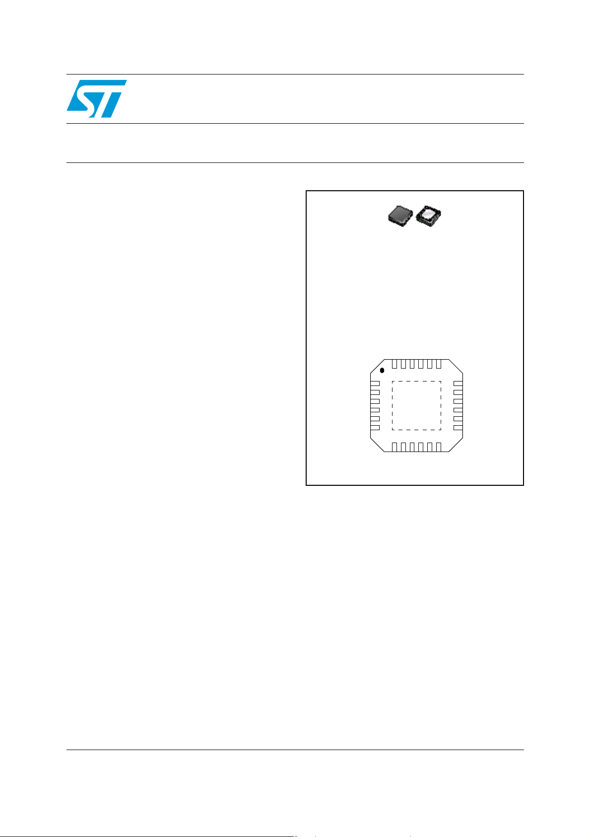
QFN 24
(Plastic micropackage)
Pin connections
(top view)
BATT
SENSE
EOCHG
BATTSENSE
PWRDETECTN
TEST
24 23 22 21 20 19
MAIN
VOUT
USBPWR
DRIVER
LDODRV
LDOFB
1
2
3
4
5
6
789101112
ISET
CVREF
The STw4102 offers dual charging capability
using separate inputs for USB cable and wall
adapter, or a single input that accepts both.
The STw4102 also offers programmable fast
charge current using an ext ernal resistor. A
thermal regulation circuit limits the charge current
against the die high power dissipation or high
ambient temperature. An e nd of charge output pin
indicates the charge termination when the fast
charge current drops below 10% of the
programmed current value.
GND
ICG+
CVIS
18
VIO
17
SCL
16
SDA
15
RESETN
14
STDBY
13
C32KHZ
ICG-
Description
The STw4102 includes an accurate gas gauge
based on a 13-bit AD converter. An external
The STw4102 is a standalone constant current
constant voltage (CCCV) linear charger
specifically designed for Li-ion batteries.
March 2008 Rev 2 1/34
resistor is used between battery and ground to
sense a charge/discharge current. With a typical
30 mΩ resistor, current can be up to 2.5 A.
www.st.com
34

Contents STw4102
Contents
1 Block diagram . . . . . . . . . . . . . . . . . . . . . . . . . . . . . . . . . . . . . . . . . . . . . . 4
2 Pin assignment . . . . . . . . . . . . . . . . . . . . . . . . . . . . . . . . . . . . . . . . . . . . . 5
3 Absolute maximum ratings and operating conditions . . . . . . . . . . . . . 6
4 Electrical characteristics . . . . . . . . . . . . . . . . . . . . . . . . . . . . . . . . . . . . . 7
Typical performance curves . . . . . . . . . . . . . . . . . . . . . . . . . . . . . . . . . . . . . . . . . 11
5 Application schematics . . . . . . . . . . . . . . . . . . . . . . . . . . . . . . . . . . . . . 14
5.1 Charge from USB or wall adapter . . . . . . . . . . . . . . . . . . . . . . . . . . . . . . 14
5.2 Charge currents higher than 1 Amp . . . . . . . . . . . . . . . . . . . . . . . . . . . . . 15
5.3 Using LDO regulator to supply telephone from wall adapter . . . . . . . . . . 16
6 Battery charger . . . . . . . . . . . . . . . . . . . . . . . . . . . . . . . . . . . . . . . . . . . . 17
6.1 Charge cycle . . . . . . . . . . . . . . . . . . . . . . . . . . . . . . . . . . . . . . . . . . . . . . 17
6.2 Trickle charge . . . . . . . . . . . . . . . . . . . . . . . . . . . . . . . . . . . . . . . . . . . . . . 18
6.3 Charging from a wall adapter . . . . . . . . . . . . . . . . . . . . . . . . . . . . . . . . . . 18
6.4 Charging from a USB port . . . . . . . . . . . . . . . . . . . . . . . . . . . . . . . . . . . . 19
6.5 Charging using external power devices . . . . . . . . . . . . . . . . . . . . . . . . . . 19
6.6 Charge mode summary . . . . . . . . . . . . . . . . . . . . . . . . . . . . . . . . . . . . . . 19
6.7 Watchdog timer . . . . . . . . . . . . . . . . . . . . . . . . . . . . . . . . . . . . . . . . . . . . 20
6.8 Thermal regulation . . . . . . . . . . . . . . . . . . . . . . . . . . . . . . . . . . . . . . . . . . 20
7 Low drop-out regulator . . . . . . . . . . . . . . . . . . . . . . . . . . . . . . . . . . . . . . 21
8 Battery monitoring . . . . . . . . . . . . . . . . . . . . . . . . . . . . . . . . . . . . . . . . . 22
8.1 Gas gauge . . . . . . . . . . . . . . . . . . . . . . . . . . . . . . . . . . . . . . . . . . . . . . . . 22
8.2 Battery voltage monitoring . . . . . . . . . . . . . . . . . . . . . . . . . . . . . . . . . . . . 23
9 Factory OTP options . . . . . . . . . . . . . . . . . . . . . . . . . . . . . . . . . . . . . . . . 24
2
10 I
2/34
C interface . . . . . . . . . . . . . . . . . . . . . . . . . . . . . . . . . . . . . . . . . . . . . . . 25
10.1 Read and write operations . . . . . . . . . . . . . . . . . . . . . . . . . . . . . . . . . . . . 25

STw4102 Contents
10.2 Register mapping . . . . . . . . . . . . . . . . . . . . . . . . . . . . . . . . . . . . . . . . . . . 26
11 Package information . . . . . . . . . . . . . . . . . . . . . . . . . . . . . . . . . . . . . . . . 31
12 Ordering information . . . . . . . . . . . . . . . . . . . . . . . . . . . . . . . . . . . . . . . 33
13 Revision history . . . . . . . . . . . . . . . . . . . . . . . . . . . . . . . . . . . . . . . . . . . 33
3/34
Block diagram STw4102
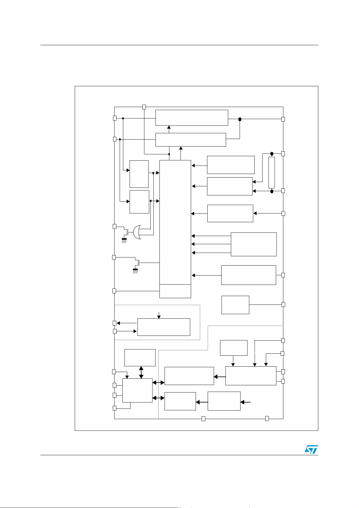
1 Block diagram
Figure 1. Internal block diagram
DRIVER
MAIN
USBPWR
PWRDETECTN
EOCHG
CVREF
Main
adapter
Detect
USB
Detect
Main Power Device (max 1A)
USB Power Device (max 500mA)
Driver
Thermal regulation
Voltage
Current
Regulation
CC/CV
Trickle threshold
Trickle current
Charge Voltage
Charge current
Vref
Current Sense
Voltage Sense
CC/CV
configuration
Current defined by
external resistor
VOUT
SENSE
Sense ressitor
BATT
BATTSENSE
ISET
LDO
LDODRV
LDOFB
Main supply
LDO driver 4.7V
Charge Control
Registers
VIO
24 bit accumulator
Control registers
SCL
SDA
RESETN
I2C interface
Control
Registers
4/34
Supply
Battery Monitoring
Power On
Reset
AD converter
7-12 bits
GND
Internal
AD converter
12 bits + sign bit
CVIS
STDBY
C32KHZ
ICG+
ICG-
Battery voltage
TEST
STw4102 Pin assignment
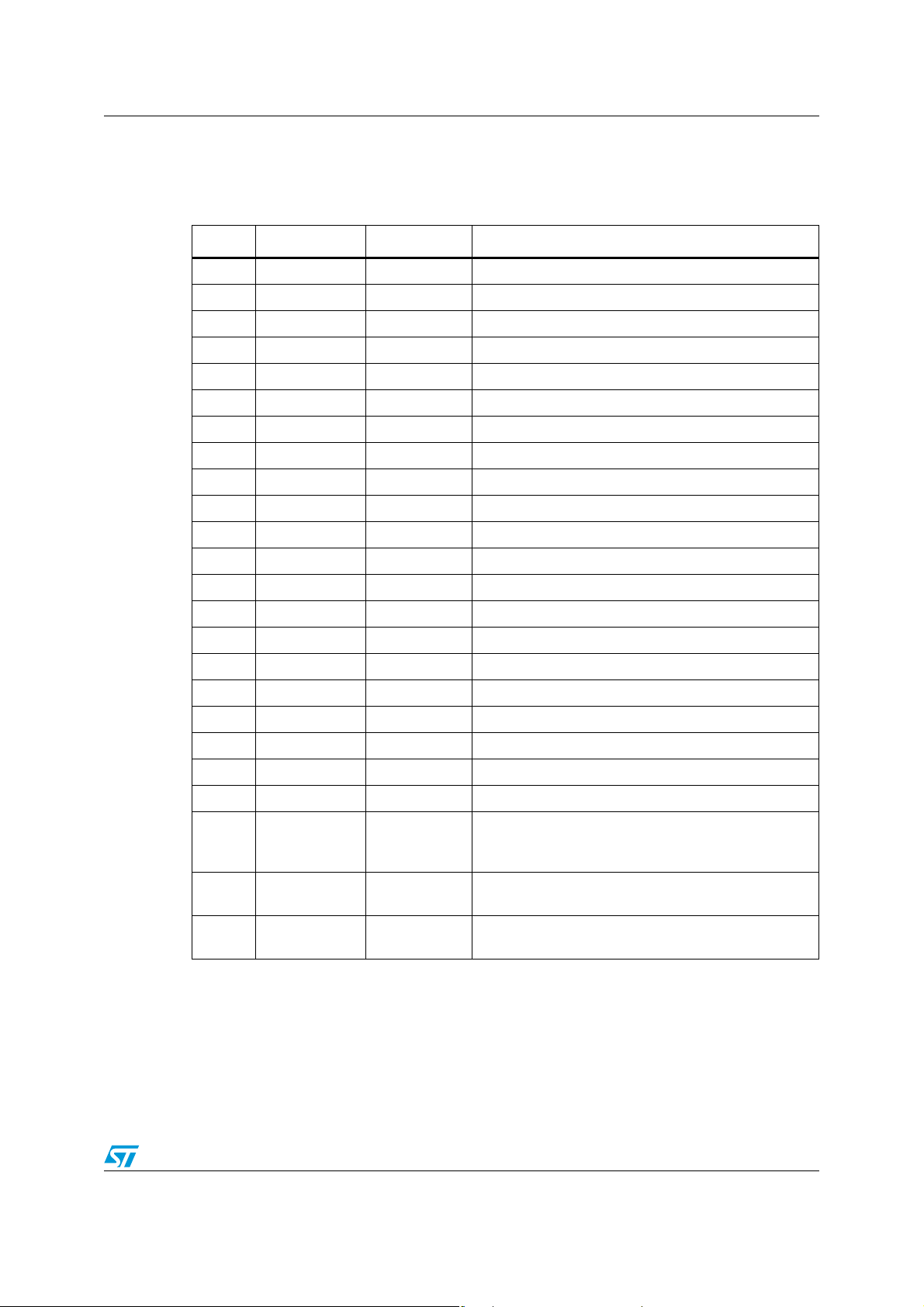
2 Pin assignment
P
Table 1. Pin descriptions
Pin # Pin name Type Function
1 MAIN Supply Main power input from wall adapter or USB charger
2 VOUT O_A Power path output
3 USBPWR Supply Power supply from USB cable
4 DRIVER O_A Driver for external power switch (PMOS or PNP)
5 LDODRV O_A LDO power PMOS driver
6 LDOFB I_A LDO feedback regulation
7 ISET O_A Resistor to program the main charge current
8 CVREF I_A Bypass capacitor for internal voltage reference
9 GND Ground Analog and digital ground
10 CVIS I_A Bypass capacitor for internal supply
11 ICG+ I_A Gas gauge sense resistor
12 ICG- I_A Gas gauge sense resistor
13 C32KHZ I_D External 32kHz clock input
14 STDBY I_D Gas gauge standby input (active low)
15 RESETN I_D Digital register reset (active low)
2
16 SD A IO_D I
17 SCL I_D I
18 VIO Supply Supply for I/O
19 SENSE I_A Sense resistor input to regulate the charge current
20 BATT Supply Battery power voltage
21 BATTSENSE I_A Battery sense voltage
22 EOCHG OD
23 TEST I_D
24 PWRDETECTN OD
C serial data.
2
C serial clock.
End of charge output status. Pulled low when the fast
charge current is above 10% of its programmed
maximum value.
Reserved pin for factory test. To be connected to
ground.
Main or USB plug-in detection. Pulled low when power
is detected, open when no power is detected.
In this table, the following conventions are used:
I: Input
O: Output
I/O: Bidirectional
OD: Open Drain
A: Analog
D: Digital
5/34
Absolute maximum ratings and operating conditions STw4102
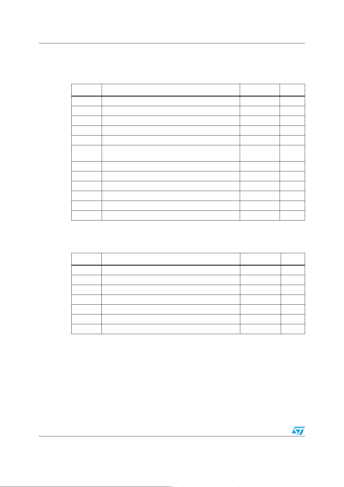
3 Absolute maximum ratings and operating conditions
Table 2. Absolute maximum ratings (AMR)
Symbol Parameter Value Unit
V
MAIN
V
CC
V
USB
V
batt
V
V
DD
P
I
sense
T
stg
T
R
thja
ESD Electrostatic discha rg e (HBM human body model)
1. Package's exposed pad is soldered to a copper pad on the PCB with multiple vias to the ground plane.
2. Human body model: 100pF discharged through a 1.5 kΩ resistor between two pins of the device, done for
all couples of pin combinations with other pins floating.
Table 3. Operating conditions
Maximum supply voltage on MAIN input 20 V
Voltage on EOCHG, LDODRV, DRIVER pins -0.3 to V
Maximum supply voltage on USBPWR input 7 V
Maximum voltage on BATT, BATTSENSE, PWRDETECTN 7 V
Maximum supply voltage on VIO pin 7 V
IO
Voltage on I/O pins (SCL, SDA, RESETN, C32KHZ,
STDBY)
Pow er dissipation self-limited
d
-0.3 to V
Maximum current from SENSE to BATT 1 A
Storage temperature -55 to 150 ° C
Maximum junction temperature 150 ° C
j
Thermal resistance junction-ambient
(1)
(2)
MAIN
IO
V
V
45 ° C/W
2kV
Symbol Parameter Value Unit
V
V
T
V
V
V
V
main
CC
USB
batt
out
oper
Operating supply voltage on MAIN 4.25 to 16 V
Maximum voltage on EOCHG 16 V
Operating supply voltage on USBPWR 4.25 to 5.5 V
Operating supply voltage on VIO 1.45 to 3.0 V
IO
Max voltage on BATT, BATTSENSE, PWRDETECTN 5.0 V
Max voltage on VOUT BATT +0.7 V
Operating free air temperature range -30 to 85 ° C
6/34
STw4102 Electrical characteristics
4 Electrical characteristics
Table 4. CC/CV charger - V
oper
=5V, V
=3.6V, T
batt
= -30°C to 85° C (unless otherwise
amb
specified)
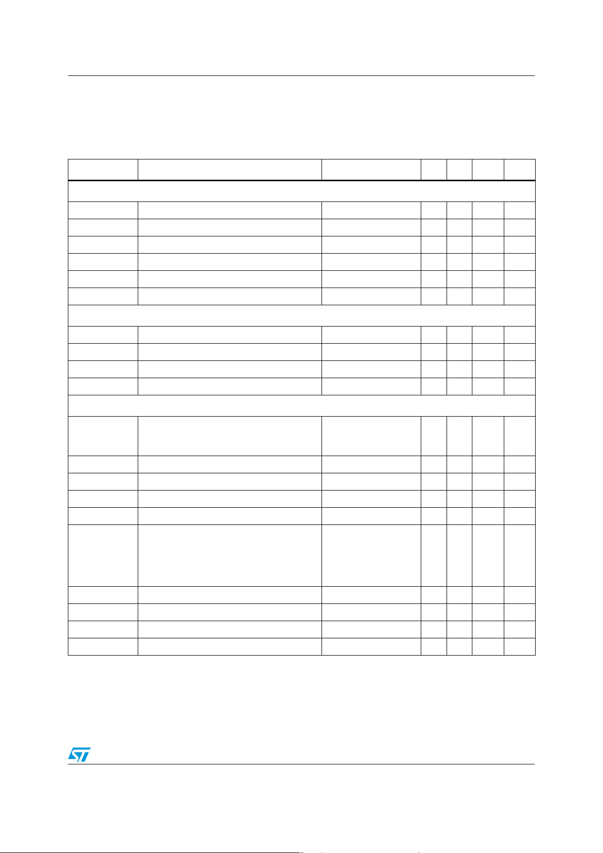
Symbol Parameter Conditions Min Typ Max Unit
Supply (V
I
charger
I
STBY
I
batt_sense
I
batt
POR_IS+ Power ON reset threshold+ CVIS internal supply 2.2 2.3 2.4 V
POR_IS- Po wer ON reset threshold- CVIS internal supply 2.1 2.2 2.3 V
Voltage regu lation
V
charge_acc
R
power
Battery
Battery
Current regulation
I
trickle
V
trickle
V
trickle_hyst
I
charge
I
charge_acc
I
USB
EOCHG
EOCHG
T
regulation
T
softstart
from MAIN or USB)
oper
Main or USB input operating current 2 mA
USBPWR input standby current Charge off 40 µA
BSENSE input current No charge 1 µA
BATT input current No charge 25 µA
Output voltage accuracy T
Power path resistance MAIN to BATT 0.6 Ω
ovv
ovv_hyst
Static battery overvoltage detection 4.55 4.7 4.8 V
Static battery overvoltage hysteresis 100 mV
Trickle charge current
Trickle to fast charge threshold Standard configuration 2.8 2.9 3.0 V
Trickle to fast charge threshold hysteresis 100 mV
Main charge current range Internal path 100 1000 mA
Main charge current accuracy I
USB charge current
ith
ith_hys
End of charge threshold % of current setting 10 %
End of charge threshold hysteresis % of current setting 5 %
Regulated junction temperature 125 ° C
Soft start from trickle to fast charge 100 µs
= 0°C to 85° C-1 +1%
amb
V
batt<Vtrickle
Standard configuration
Factory OTP option
> 500mA -15 +15 %
charge
306060
120
100
180mAmA
REG_CHG0[7..6]:
00
01
10
11
30 60
200
400
100
500
0
mA
mA
mA
mA
7/34
Electrical characteristics STw4102
Table 4. CC/CV charger - V
oper
=5V, V
=3.6V, T
batt
= -30°C to 85° C (unless otherwise
amb
specified) (continued)
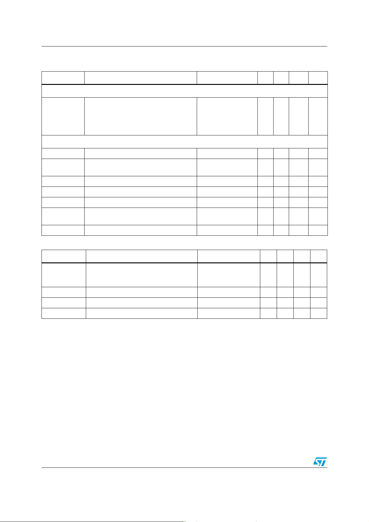
Symbol Parameter Conditions Min Typ Max Unit
Watchdog
REG_WDOG[2,1]:
00
t
watchdog
Watchdog duration
01
10
11
Input/output pins
V
charger_det
V
charger_det_hys
V
USB_det
V
USB_det_hys
Vol
powerdetect
Vol
EOCHG
I
drv_sink
Table 5. LDO - V
Main charger supply voltage detection 2.4 2.5 2.6 V
Main charger supply voltage detection
hysterisis
USB supply voltage detection 2.4 2.5 2.6 V
USB supply voltage detection hysteresis 100 mV
POWERDETECTN output capability I
EOCHG output capability
= 10mA 0.45 V
sink
= 10mA
I
sink
= 20mA
I
sink
Driver sink current (If option enabled) 60 mA
main
=6V, T
= -30°C to 85° C (unless otherwise specified)
amb
Symbol Parameter Conditions Min Typ Max Unit
0.5
1
7.5
15
15
30
30
60
100 mV
1.5
22.5
45
90
0.5
1.1
min
min
min
min
V
V
LDO
LDO
LDO
LDO
V
power_th
power_th_hys
PSRR
Including line and load
LDO regulated output voltage
regulation (up to 1A),
V
>6V
main
4.47 4.7 4.93 V
LDO power turn off threshold 6.8 7.2 7.5 V
LDO power turn off threshold hysterisis 0.7 V
LDO power supply rejection ratio Up to 20kHz 50 dB
8/34
STw4102 Electrical characteristics
Table 6. Battery monitor - V
=3.6V, T
batt
= -30°C to 85° C (unless otherwise specified)
amb
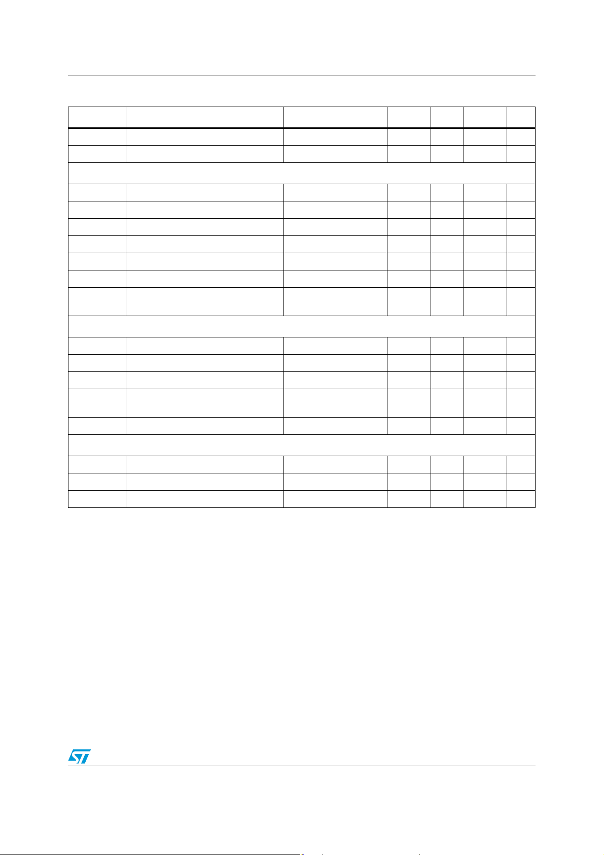
Symbol Parameter Conditions Min Typ Max Unit
POR_IS2+ Power ON reset threshold+ CVIS internal supply 2.6 2.7 2.8 V
POR_IS2- Power ON reset threshold- CVIS internal supply 2.5 2.6 2.7 V
Gas gauge A/D converter
V
os_gg
V
in_gg
I
dd_gg
I
pdn_gg
I
in
LSB
Acc
gg
Tamb_gg
Input offset voltage 40 µV
Input voltage range -80 +80 mV
Current consumption CG_ENA=1 90 µA
Current consumption in off mode CG_ENA=0 1 µA
Input current for ICG+ and ICG- 500 nA
AD converter granularity (LSB value) 12 bits + 1 sign bit 23.5 µV
Accuracy at ambient temperature
External resistor at 1%
No calibration
3%
Battery voltage A/D converter
V
in_mon
I
dd_mon
I
pdn_mon
LSB
mon
Acc
Tamb_m on
Input voltage range BATT voltage 1 5 V
Current consumption ADPOWERON=1 190 µA
Current consumption in off mode ADPOWERON=0 1 µA
AD converter granularity (LSB value)
7 bits
12 bits
45.4
1.42
Accuracy at ambient temperature No calibration 3 %
Digital I/O pins (SCL, SDA, STDBY, C32KHZ, RESETN)
mV
mV
V
il
V
ih
V
ol
Input pin low voltage 0 0.3 x V
Input pin high voltage 0.7 x V
SDA output pin low voltage I
= 3mA 0.2 x V
sink
IO
V
IO
V
IO
V
V
IO
9/34
Electrical characteristics STw4102
Table 7. I
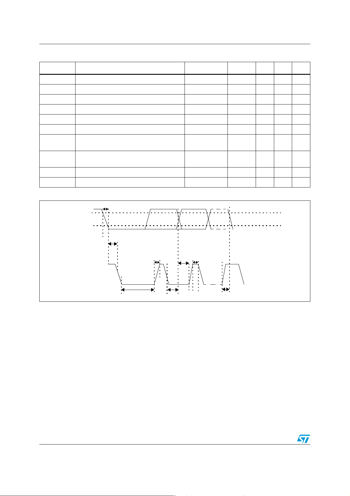
Symbol Parameter Conditions Min Typ Max Unit
2
C timing - VIO= 2.8V, T
= -30°C to 85° C (unless otherwise specified)
amb
F
scl
t
hd,sta
t
low
t
high
t
su,dat
t
hd,dat
t
r
t
f
t
su,sto
C
b
SCL clock frequency 400 kHz
Hold time (repeated) START condition 0.6 µs
LOW period of the SCL clock 1.3 µs
HIGH period of the SCL clock 0.6 µs
Setup time for repeated START condition 0.6 µs
Data hold time 0 0.9 us
Rise time of both SDA and SCL signals
Fall time of both SDA and SCL signals
Setup time for STOP condition 0.6 µs
Capacitive load for each bus line 400 pF
Figure 2. I2C timing diagram
t
f
ih
il
t
hd,sta
SDA
V
V
20+
0.1C
20+
0.1C
b
b
300 ns
300 ns
SCL
t
low
t
hd,dat
t
su,dat
t
high
t
su,sta
t
r
10/34
STw4102 Electrical characteristics
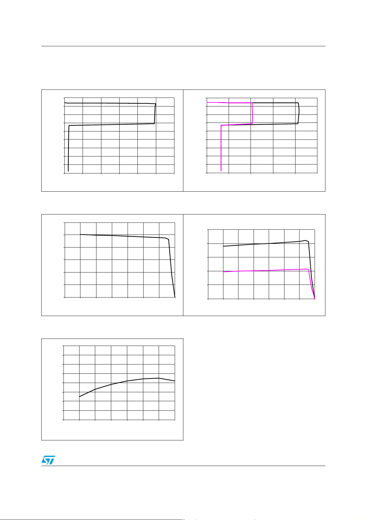
Typical performance curves
Figure 3. Charger voltage vs. charge current
(Main charge, 4.2V and 1A settings)
4.5
4.0
3.5
3.0
2.5
2.0
Vba tt (V)
1.5
1.0
0.5
0.0
0 200 400 600 800 1000 1200
Icharge (mA)
Figure 5. Charge current vs. tempe rat u r e
(charge from MAIN, 1A setting)
1.2
1.0
0.8
0.6
Icharge (A)
0.4
Figure 4. Charger voltage vs. charge current
(USB charge, 4.2V setting)
4.5
4.0
3.5
3.0
2.5
2.0
Vba tt (V)
1.5
1.0
0.5
0.0
0 100 200 300 400 500
Iusb (mA)
Ich=400mAIch=200mA
Figure 6. Charge current vs. temperature
(charge from USBPWR)
500
400
300
200
Iusb (mA)
Ich=400mA
Ich=200mA
0.2
0.0
-50-250 255075100125
Temp (°C)
Figure 7. Charge voltage vs. temperature
(4.2V nominal setting)
4.24
4.23
4.22
4.21
4.20
4.19
Vcharge (V)
4.18
4.17
4.16
-50 -25 0 25 50 75 100 125
Temp (°C)
100
0
-50 -25 0 25 50 75 100 125
Temp (°C)
11/34

Electrical characteristics STw4102
Figure 8. USB standby input current vs.
temperature (charge disabled)
60
50
40
30
Iusb (µA)
20
10
0
-50 -25 0 25 50 75 100 125
Temp (°C)
Figure 10. Watchdog period vs. temperature
(normalized to value at 25°C)
1.4
1.2
Figure 9. Battery standby current vs
temperature (no MAIN, no
USBPWR, gas gauge disabled)
60
50
40
30
Ibat (µA)
20
10
0
-50 -25 0 25 50 75 100 125
Temp (°C )
Figure 11. LDO output voltage vs. temperature
(10 mA output current)
4.9
4.8
1.0
Twatchdog
0.8
0.6
-50-250 255075100125
Temp (°C)
Figure 12. LDO output voltage vs. output
current
5.0
4.9
4.8
4.7
LDOv (V)
4.6
4.5
4.4
0 500 1000 1500
LDOi (mA )
Vmain=6V
Vmain=5V
4.7
LDOv (V)
4.6
4.5
-50 -25 0 25 50 75 100 125
Temp (°C)
12/34

STw4102 Electrical characteristics
Figure 13. Waveforms at USB plug-in
Vusb
Vbatt
Ibatt
50µs/div
Figure 14. Switching from USB char ge to main
charge
Vmain
Vbatt
Ibatt
100µs/div
Figure 15. Switching from main char ge to USB
charge
Vmain
Vbatt
Ibatt
10ms/div
13/34

Application schematics STw4102
5 Application schematics
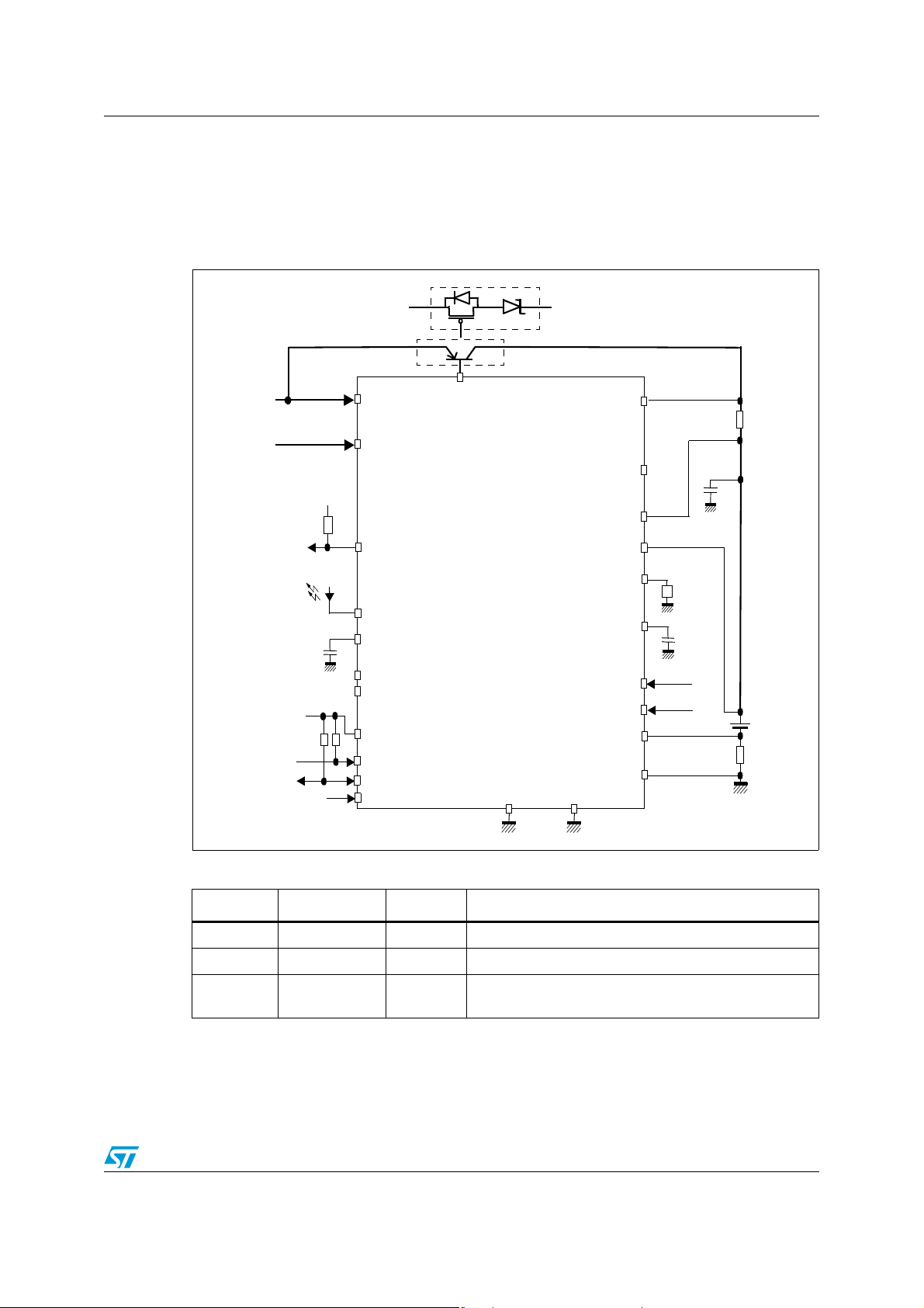
5.1 Charge from USB or wall adapter
The MAIN input is used with either a wall adapter or a USB charger. The charge current can
be programmed to 100 mA or 500 mA max for use with a USB 2.0 port, or programmed to
the value set by the R
The USBPWR input is used only for charging from a USB port (100 mA or 500 mA max).
Figure 16. Charge using internal power devices
resistor for use with a wall adapter or a dedicated USB charger.
set
from wall adapter
or USB port/charger
from USB port only
battery voltage
to power
management
Indicator LED
Reset
C4
C5
C2
IO voltage
MAIN
USBPWR
PWRDETECTN
EOCHG
CVREF
LDODRV
LDOFB
VIO
SCL
SDA
RESETN
DRIVER
STw4102
GND
VOUT
SENSE
BATTSENSE
C32KHZ
STDBY
TEST
BATT
ISET
CVIS
ICG+
ICG-
C3
Rset
C1
32kHz
StandBy
Rcg
Table 8. External component list
Name Typ. value Tolerance Comments
R
set
R
cg
12k to 120k 1% Main charge current setting
30mΩ 1% Gas gauge sense resistor
C1 1µF Internal supply decoupling capacitor
C2 1µF Internal voltage reference decoupling capacitor
C3 0.1 to 22µF
C4 0.1 to 1µF MAIN input decoupling capacitor
C5 0.1 to 1µF USBPWR input decoupling capacitor
14/34
When the battery is removed, a capacitor of at least
15µF is required for low ripple on the battery line.
STw4102 Application schematics
5.2 Charge currents higher than 1 Amp
One-time programming (OTP) options off er the ab ility to use an external power device or an
external sense resistor to handle charge currents higher than 1 A from the wall adapter.
These OTP options are set by STMicroelectronics at factory level.
Figure 17. Charge using e xternal power devices
D1
M1
T1
battery voltage
to power
management
Indicator LED
IO voltage
Reset
C2
MAIN
USBPWR
PWRDETECTN
EOCHG
CVREF
LDODRV
LDOFB
VIO
SCL
SDA
RESETN
DRIVER
STw4102
GND
VOUT
SENSE
BATT
BATTSENSE
ISET
CVIS
C32KHZ
STDBY
ICG+
ICG-
TEST
Rs
C3
Rset
C1
32kHz
StandBy
Rcg
Table 9. Component list for external power devices
Name Typ. value Tolerance Comments
R
set
R
s
T1 or
M1 + D1
8k to 12k 1% Main charge current setting
200mΩ 1% External current sense resistor
STT818B
STS2DPFS20V
PNP transistor
PMOS transistor with Schottky diode
15/34
Application schematics STw4102
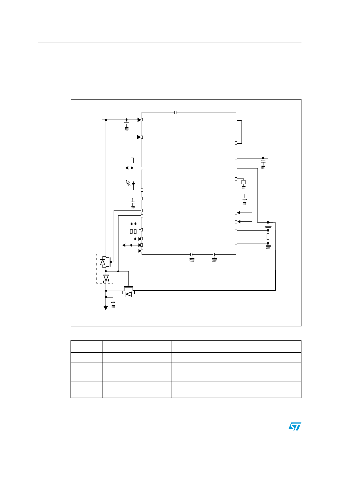
5.3 Using LDO regulator to supply telephone from wall adapter
The regulator with external power PMOS (M1) supplies the telephone while the battery is
discharged or unplugged. When the charger is unplugged, the phone is supplied by the
battery through Power MOS M2. A Schottky diode (D1) avoids reverse current.
Figure 18. Charge power path and regulator
to power
management
M1
D1
C4
Battery voltage
Indicator LED
C2
IO voltage
Reset
MAIN
USBPWR
PWRDETECTN
EOCHG
CVREF
LDODRV
LDOFB
VIO
SCL
SDA
RESETN
DRIVER
STw4102
GND
VOUT
SENSE
BATT
BATTSENSE
ISET
CVIS
C32KHZ
STDBY
ICG+
ICG-
TEST
C3
Rset
C1
32kHz
StandBy
Rcg
M2
Co >= 15uF
To phone
Table 10. Component list for LDO regulator
Name Typ. value Tolerance Comments
M1 + D1 STS2DPFS20V PMOS transistor with Schottky diode
M2 STT5PF20V PMOS transistor
Co 10µF to 22µF An output capacitor Co of at least 10µF is required.
C4 Co
16/34
An input capacitor C4 equal to or larger than Co is
required on MAIN input.

STw4102 Battery charger
6 Battery charger
6.1 Charge cycle
The charge cycle is initiated when the presence of a power source on either the MAIN or
USBPWR inputs is detected (the PWRDETECTN pin goes low), while the charger is
enabled by the CHG_ENA bit of the REG_CHG1 control register. If both supplies are
connected, the MAIN input path is selected.
The EOCHG output pin is driven low as the charge begins. If the battery voltage is lower
than the trickle threshold, the charge cycle begins in t ric kle m ode wit h a low current (default
value: 60 mA) until the battery voltage reaches the trickle voltage threshold (default value:
2.9 V). Once the battery voltage rises above this threshold, the charger enters into fast
charge mode where the programmed charge current I
battery.
When the battery voltage approaches the programmable charge voltage (4.10V, 4.20V,
4.30V or 4.35V), the charger enters int o a constant v olta ge charging mode and the chargi ng
current decreases. When the current level reaches the end-of charge level (10% of I
the EOCHG status pin is switched off (open) to indicate that the battery is almost fully
charged, and the charger enters maintenance mode.
charge
or I
is supplied to the
USB
charge
),
In maintenance mode, the charger continues to monitor the battery voltage to maintain the
battery voltage level. The maintenance mode lasts until the charge is stopped by clearing
the CHG_ENA bit in the REG_CHG1 control register, or by removing the power source
(PWRDETECTN is opened).
Figure 19. Charge flow (simplified)
EOCH OPEN (LED OFF)
Power detected (PWRDETECTN LOW)
Trickle charge
EOCH LOW (LED ON)
V
< 2.8v
batt
CCCV charge
EOCH LOW (LED ON)
> 15%
I
charge
Maintenance charge
EOCH OPEN (LED OFF)
CCCV is still ON
Charge Off
60mA
V
batt
I
charge
> 2.9v
< 10%
Power removed (PWRDETECTN OPEN)
Charge Stopped
EOCH OPEN (LED OFF)
Battery overvoltage
or Watchdog event
Battery overvoltage
or Watchdog event
17/34

Battery charger STw4102
6.2 Trickle charge
The trickle charge mode is enabled when the battery voltage V
voltage threshold V
above V
, the trickle current generator is off and the battery is charged using the
trickle
. An internal current source charges the battery. When V
trickle
constant current method.
The trickle voltage threshold and trickle current are defined by OTP configuration bits and
are factory set to 2.9 V and 60 mA b y default. Other values are possible, see Section 9:
Factory OTP opt ions on page 24.
6.3 Charging from a wall adapter
The MAIN input is used for charging from a wall adapter or a dedicated USB charger. The
SEL_DC_USB bit (bit 5 of register REG_CHG0) must be set to 0. The fast charge current is
defined by the external resistor R
The value of the fast charge current is given by the following formula:
I
= 12000 / R
charge
set
In the constant voltage mod e, the ch arger output v oltag e is regulated with 1% accur acy. The
charger output voltage is programmable using the REG_CHG0 register, bits 3 and 4 (see
Table 11).
Table 11. Charger output vol tage
REG_CHG0[4] REG_CHG0[3] V
0 0 4.10V +/- 1%
connected to the ISET pin, and can be set up to 1 A.
set
is lower than the trickle
batt
batt
charge
is
0 1 4.20V +/- 1%
1 0 4.30V +/-1%
1 1 4.35V +/-1%
Figure 20. Main charge mode
I
batt
I
I
trickle
charge
set
(60mA)
)
Trickle
charge
Constant current
(defined by R
Battery Voltage
Charge current
Fast charge
Flag end of
charge (10% I
Constant voltage
charge
Maintenance
charge
V
batt
V
charge
)
V
(2.9v)
trickle
18/34

STw4102 Battery charger
6.4 Charging from a USB port
The MAIN or USBPWR input can be used to charge from a USB 2.0 port. When using the
MAIN input, bit SEL_DC_USB (bit 5 of register REG_CHG0) must be set to 1. Charging
from a USB port is similar to charging from a wall adapter, except the fast charge current
I
is set internally and depends on bits 6 and 7 of the control register REG_CHG0.
USB
Table 12. USB charge current
REG_CHG0[7] REG_CHG0[6] I
0 0 60mA (100 mA max)
0 1 200mA
1 0 400mA (500 mA max)
11 off
6.5 Charging using external power devices
To support charge currents higher than 1 A from the main supply adapter, the STw4102
provides the option to use an external power device and sense resistor. This OTP option is
factory set.
The STw4102 driver is able to drive an external PNP (STT818B or equivalent) or a PMOS
plus Schottky diode (STS2DPFS20V or equivalent). The driver maximum sink current is
60 mA.
The external current sensing device is usually a 200 mΩ shunt resistor. With this resistor
value, the trickle and USB charge currents are close to the nominal values.
6.6 Charge mode summary
Table 13 summarizes the different charge modes.
Table 13. Charge modes
USB
(typ)
V
batt
-
under
V
trickle
above
V
trickle
MAIN
detected
0 0 1 x No charge
1x
0 1 Trickle charge from USBPWR
1x
0 1 1 x
USBPWR
detected
x x 0 x Charge disabled
CHG_ENA
bit
1x
10
11
SEL_DC_USB
bit
19/34
Charge
Trickle charge from MAIN
Fast charge from MAIN input,
current set by Rset
Fast charge from MAIN input,
current set by USB_ICHG bits
Fast charge from USBPWR input,
current set by USB_ICHG bits

Battery charger STw4102
6.7 Watchdog timer
When the fast charge is active, a watchdog timer starts to prevent damage on the battery.
The system controller refreshes the watchdog periodically in order let the charge continue.
When the watchdog time elapses, the charge is stopped.
When the charge starts in trickle mode, to allow the battery to be charged although the
system controller is not running, the watchdog is disabled. However, if for any reason the
charger goes from fast charge mode to trickle mode, then the watchdog is not disabled to
protect against battery failure.
Watchdog timing ca n be 1 minute , 15 minutes , 30 minut es or 60 minutes . It is progr ammable
through the I
or by unplugging the charger (PWRDETECTN goes to low). The watchdog can also be
enabled and disab led through the I
In the standard configuration, t he default state at powerup is watchdog enabled and the
timing is one minute.
2
C interface. The w atc hdog ca n be rese t b y t he I2C interface (bit WDOG_RST)
6.8 Thermal regulation
A thermal regulation circuit limits the charge current in case of high po wer dissipation due to
high input voltage or high ambient temper ature. Th e charge current is prog ressively red uced
to maintain the die temperature in a safe area. This allows to charge the battery with the
highest possible current depending on the operating conditions, and protects the device
against any damage.
2
C interface.
20/34

STw4102 Low drop-out regulator
7 Low drop-out regulator
The purpose of the low drop-out regulator (LDO) is to supply t he phone directly from t he wall
adapter when the battery is low or not present. When the wall adapter is present, MOSFET
is off and the phone supply is regulated at 4.7 V minus the drop voltage across D1. When
the MAIN pin is not connected, MOSFET M2 is on (the gate is pulled down) and the D1
diode avoids any reverse current. The LDO output current is limited by The M1 MOSFET
and D1 diode current capabilities. An output capacitor C
schematics are illustrated in Figure 21.
When the battery is fully discharged, the regulator can charge the battery from the main
supply and at the same time supply the phone, which avoids waiting for the battery to be
charged up to the minimum operating voltage before using the phone.
Figure 21. Regulator
Wall adapter power supply
of at least 15 µF is required. The
o
M1
To phone
LDODRV
LDOFB
D1
M2
Co >= 15uF
When the main supply is abov e the low dropout threshold LDO
Main supply
LDO 4.7V
Battery power supply
power_th
(about 7.2 V), then
the LDO is turned off to protect the ext ernal PMOS against high po wer dissip ation as sho wn
in Figure 22. LDO
power_th
hysteresis is around 0.7 V. By default, this protection feature is
enabled, but can be disabled at factory level by OTP.
Figure 22. Supply voltage
Main supply voltage
7.2V
6.5V
4.7V
Main detect
ON
ON
21/34

Battery monitoring STw4102
8 Battery monitoring
8.1 Gas gauge
The gas gauge is designed to monitor the battery capacity. A current sensing resistor
(typically of 30 mΩ) is needed between the negative terminal of the battery and the ground.
The sensing resistor voltage drop is input to a 13-bit integrating AD converter. When a
conversion cycle is completed, depending on the output sign, the result is forwarded to the
charge or discharge 24-bit accumulator, and the number of conversions is incremented in a
12-bit counter.
One accumulator accumulates current fl owing into the batt ery during charging and the other
accumulates discharge current during system operation. The rema ining battery charge is
given by the difference between the charge and discharge accumu lators.
Figure 23. Gas gauge block diagram
ICG+
ICG-
AD converter
12 bits + sign bit
From 2’s
to binary
EOC
cg_clock
cg_enable
cg_calibration
sign
24 bit max
Σ
32kHz
12 bits Counter
Charge
accumulator
Control logic
Discharge
accumulator
Control
registers
Conv_number
registers
13
24
24
Conv_data
registers
Charge
registers
Discharge
registers
The Digital Base Band (DBB) can control, enable and read gas gauge data t hrough I
control registers. The DBB can read the value of the most recent conversion in two’s
complement format by reading the CONVDATA registers.
The RD_REQ bit enables the transfer of the charge/discharge accumulators and con v ersion
counter register. The transfer can take up to eight 32 kHz cycles, therefore a delay of
22/34
2
C

STw4102 Battery monitoring
approximately 250 microseconds must be respected between the time the RD_REQ bit is
set and the actual register reading. The RD_REQ bit is automatically cleared after the
transfer.
A high value written to the RST_CHRG, RST_DCHRG or RST_COUNTER bits of the
control register resets respectively the charge accumulator, discharge accumulator or
conversion counter. If these bits are set together with the RD_REQ bit, then the reset occurs
after the transfer to the charge, discharge or conversion counter register respectively. The
RST_CHRG, RST_DCHRG or RST_COUNTER bits are automatically cleared after the
reset.
The differential inputs are scaled to the full range of the AD converter, introducing a small
offset error. A high value written to the CG_CAL bit of the control register connects the
inputs of the AD converter together, allowing the DBB to measure the digital offset error.
Using this measurement, the gas gauge can be calibrated to reduce the offset error.
The conversion cycle of a 12- bit plus 1 sign-bit AD converter is 2
13
(8192) clock cycles.
Using the 32.768kHz RTC clock, the conversion cycle time is 250 ms. The LSB value is
23.54 µV, which corresponds to a current of 784.7 µA with a typical 30 mΩ sense resistor.
Given a 250 ms con v ersion cycle time, this LSB v alu e corresponds t o a charge of 54.5nAh.
Under these conditions, the 24-bit accumulator has a capacity of 914 mAh.
The gas gauge system is disabled when the battery voltage is below the Power On Reset
threshold (2.7 V), or when the RESETN pin is driven low (CG_ENA bit default value is 0).
During normal operation, either the STDBY pin or the CG_ENA bit can be used to disab le
the gas gauge function. When the STDBY pin is low, the gas gauge is disabled without
waiting for the end of the current conversion. When the CG_ENA bit is low, the current
gauge is disabled at the end of the current conversion.
8.2 Battery voltage monitoring
The battery voltage can be measured by mean s of a 7- or 12-bit A/D con v erter. This funct ion
is enabled and configured using the following bits of the ADCTRL register:
● The ADPOWERON bit enables battery voltage monitoring.
● The ADRESOLUTION bit allows to select 7- or 12-bit conversion.
● The ONSTATE bit is set when the ADC converter is ready.
● The ADSTART bit starts a conversion; it is automatically cleared after writing.
● The ADRUN bit indicates that a conversion is in progress. The result is available when
the ADRUN bit goes low, and it can be read in the ADDATA registers.
A high value written to the ADCAL bit of the control re gister connects the input of the A/D
converter to ground, allowing the DBB to measure the digital offset error. Using this
measurement, the AD converter can be calibrated to reduce the offset error.
The conversion cycle of a 7 (12) bit co nv ersion is 2
32.768kHz RTC clock, the conversion cycle time is 7.8 (250) ms. LSB va lue is 45 (1.4) mV.
When the battery voltage falls below the Power On Reset threshold, or when the RESETN
input is driven low, the battery voltage monitoring function is disabled.
8
=256 (213=8192) clock cycles. Using the
23/34

Factory OTP options STw4102
9 Factory OTP options
Table 14 summarizes the one-time programming (OTP) options offered by
STMicroelectronics to customize the STw4102 at factory level.
Table 14. Factory OTP options
Option Configuration bits Value
TRICKLE current (wall adapter
charge only)
TRICKLE threshold voltage
MAIN input mode at powerup
Watchdog state at powerup
Watchdog period at powerup
Power switch
Sense resistor
LDO overvoltage protection
OTP_TC=0 (default)
OTP_TC=1
OTP_TV1, OTP_TV 0 :
00
01
10
11 (default)
OTP_SEL_DC_USB=0 (default)
OTP_SEL_DC_USB=1
OTP_WD_ENA=0
OTP_WD_ENA=1 (default)
OTP_WD_TIME1, O T P_WD_TIME0 :
00 (default)
01
10
11
OPT_IEPD=0 (default)
OPT_IEPD=1
OPT_IERSENSE=0 (default)
OPT_IERSENSE=1
OPT_LDOEXT_PRO=0
OPT_LDOEXT_PRO=1 (default)
60 mA
120 mA
2.3 V
2.5 V
2.7 V
2.9 V
Wall adapter mode
USB mode
Disabled
Enabled
1 min
15 min
30 min
60 min
Internal
External
Internal
External
Disabled
Enabled
OTP_ID2, OTP_ID1, OTP_ID0 :
000 (default)
001
2
C ID address
I
010
011
100
101
110
111
For any option re quest other than the standard configuration (default values), contact
STMicroelectronics to get a specific order code.
24/34
70h
71h
72h
73h
74h
75h
76h
77h

STw4102 I2C interface
10 I2C interface
10.1 Read and write operations
The I2C interface is used to control the ch arging an d the ga s gauge system. I t is compatib le
with the I
2
C specification of Philips (version 2.1). It is a slave serial interface with a serial
data line (SDA) and a serial clock line (SCL):
SCL: input clock used to shift data
SDA: input/output bi-directional data transfers
A filter rejects the potential spikes on th e bus data line to preserve data integrity. The bidirectional data line supports transfers up to 400 kbit/s (fast-mode). The data is shifted into
and from the chip on the SDA line, MSB first.
The first bit must be high (START), followe d by the De vice ID an d Read/Write control bit (see
Table 15). The AddrID0 to AddrID2 bits are factory programmable, their default ID value is
70h (AddrID0 = AddrID1 = AddrID2 = 0). Then, the STw4102 sends an acknowledge at the
end of the 8-bit transmission.
The next 8 bits correspon d to the address register, followed by another acknowledge.
Table 16 shows the address register format.
The data field is sent last. It can be composed of several 8-bit data registers, each followed
by an acknowledge. Table 17 shows the data register for m at.
The STw4102 supports byte read, word read, block read, and byte write operations. The
transmission protocol is summarized in Figure 24 and Figure 25.
Table 15. Device ID and R/W bit format
b7 b6 b5 b4 b3 b2 b1 b0
1 1 1 0 AddrID2 AddrID1 AddrID0 R/W
Table 16. Address register format
b7 b6 b5 b4 b3 b2 b1 b0
RegAddr7 RegAddr6 RegAddr5 RegAddr4 RegAddr3 RegAddr2 RegAddr1 RegAddr0
Table 17. Data register format
r
b7 b6 b5 b4 b3 b2 b1 b0
DATA7 DATA6 DATA5 DATA4 DATA3 DATA2 DATA1 DATA0
Figure 24. Byte, word and block read operation
Master
Start Device id
7 bits 7 bits
Start bit = SDAfalling w h en SCL=1
Stop bit = SDArising when SCL=1
Restart bit = start after a start
Acknowledge = SDA force low during a SCL clock
Slave
W
Reg address
A
8bits
A
Restart Device id
Reg data
A
R
8bits
<-- byte read -->
<-- word read (2 bytes) ---------->
<-- block read (up to 10 bytes) ---------------------->
A
Reg data
8bits
address
n+1
A
Reg data
8bits
address
n+2
A/A
25/34
Stop

I2C interface STw4102
Figure 25. Byte write operati on
Start Device id
7 bits
Start bit = SDAfalling when SCL=1
Stop bit = SDArising when SCL=1
Restart bit = start after a start
W
A
10.2 Register mapping
The mapping of all registers is shown in Table 18. Individual register descriptions are sho wn
in Table 19 to Table 35. Power-up values are set at power startup, or at reset (RESETN pin
falling edge). Charge and discharge internal accumulators are not affected by RESETN.
Table 18. Register mapping
Name
REG_CHG0 0 Charge control and status
REG_CHG1 1 Charge enable
REG_WDOG 2 Watchdog control
REG_CG 3 Gas gauge control
REG_CHARGE_LOW 4 Gas gauge charge data, bits 0-7
Reg address
8bits
Address
(dec.)
A
Reg data
8bits
A
Stop
Description
REG_CHARGE_MID 5 Gas gauge charge data, bits 8-15
REG_CHARGE_HIGH 6 Gas gauge charge data, bits 16-23
REG_DISCHARGE_LOW 7 Gas gauge discharge data, bits 0-7
REG_DISCHARGE_MID 8 Gas gauge discharge data, bits 8-15
REG_DISCHARGE_HIGH 9 Gas gauge discharge data, bits 16-23
REG_CONVDATA_LOW 16 Gas gauge AD converter data, bits 0-7
REG_CONVDATA_HIGH 17 Gas gauge AD converter data, bits 8-12
REG_CONVNUMBER_LOW 18 Number of conversions, bits 0-7
REG_CONVNUMBER_HIGH 19 Number of conversions, bits 8-11
REG_ADCTRL 20 Battery voltage monitor control
REG_ADDATA_LOW 21 Battery voltage monitor AD converter data, bits 0-7
REG_ADDATA_HIGH 22 Battery voltage monitor AD converter data, bits 8-10
26/34

STw4102 I2C interface
Table 19. REG_CHG0. address 0 (00h)
Name Pos. Type
CHARGERUN 0 R 0
Power-
up
Description
0: Charge is below 10% of fast charge current.
1: Charge is above 10% of fast charge current.
MAINDETECT 1 R 0 Main input voltage detection.
USBDETECT 2 R 0 USB input voltage detection.
VCHG [4,3] R/W 00
Charge voltage
00=4.1V, 01=4.2V, 10=4.3V, 11=4.35V.
Wall adapter/USB selection for MAIN input
SEL_DC_USB 5 R/W 0
0: charge current set by Rset resistor
1: charge current set by USB_ICHG bits
USB_ICHG [7,6] R/W 00
Table 20. REG_CHG1. address 1 (01h)
Name Pos. Type
Power-
CHG_ENA 0 R/W 1
USB charge current
00=60mA, 01=200mA, 10=400mA, 11=off.
up
Description
0: Charger disabled.
1: Charger enabled.
Reserved [3,1] R/W 0 Reserved bits, to be set to zero.
FORCECHARGER
UN
4R/W0
0: no effect.
1: force EOCHG low independently of charge
state.
0: Internal supply from Main or USB input when
SEL_IS 5 R/W 0
available and charge enabled.
1: Internal supply always from Battery.
Unused [7,6] R/W
Table 21. REG_WDOG. address 2 (02h)
Name Pos. Type
WDOG_EN 0 R/W 1
WDOG_TIME [2,1] R/W 00
WDOG_RST 3 R/W 0
Power-
up
Description
0: Watchdog disabled.
1: Watchdog enabled.
00=1 minute, 01=15 minutes, 10=30 minutes,
11=60 minutes.
0: No effect.
1: Reset watchdog. Bit clear after watchdog reset.
Reserved [5,4] R/W 0 Reserved bits, to be set to zero
WDOG_INT 6 R x 1: Watchdog is elapsed.
Unused 7 R/W
27/34

I2C interface STw4102
Table 22. REG_CG. address 3 (03h)
Name Pos. Type
Power-
up
0: Gas gauge disabled. Charge/discharge
CG_ENA 0 R/W 0
accumulators are reset.
1: Gas gauge enabled.
0: No effect.
RST_CHRG 1 R/W 0
1: Resets the charge accumulator. This bit auto
clears after the charge register is reset.
0: No effect.
RST_DCHRG 2 R/W 0
1: Resets the discharge accumulator. This bit auto
clears after the discharge register is reset.
0: No effect.
RST_COUNTER 3 R/W 0
1: Resets the counter conversion. This bit auto
clears after the counter register is reset.
0: No effect.
1: Transfers the 24 bit charge/discharge
RD_REQ 4 R/W 0
accumulators and the conversion counter to the
charge/discharge and conversion number
registers. This bit auto clears after the transfer.
CG_CAL 5 R/W 0
CG_EOC 6 R 0
0: No effect.
1: Allows to calibrate AD converter.
Set high at the end of a conversion. Cleared after
read.
Unused 7 R/W
Table 23. REG_CHARGE_LOW. address 4 (04h)
Description
Name Pos. Type
Power-
up
Description
DATA[7..0] [7..0] R 00 Current charge data.
Table 24. REG_CHARGE_MID. address 5 (05h)
Name Pos. Type
Power-
up
Description
DATA[15..8] [7..0] R 00 Current charge data.
Table 25. REG_CHARGE_HIGH. address 6 (06h)
Name Pos. Type
Power-
up
Description
DATA[23..16] [7..0] R 00 Current charge data.
Table 26. REG_DISCHARGE_LOW. address 7 (07h)
Name Pos. Type
Power-
up
Description
DATA[7..0] [7..0] R 00 Current discharge data.
28/34

STw4102 I2C interface
Table 27. REG_DISCHARGE_MID. address 8 (08h)
Name Pos. Type
Power-
up
Description
DATA[15..8] [7..0] R 00 Current discharge data.
Table 28. REG_DISCHARGE_HIGH. address 9 (09h)
Name Pos. Type
Power-
up
Description
DATA[23..16] [7..0] R 00 Current discharge data.
Table 29. REG_CONVD ATA_LOW. address 16 (10h)
Name Pos. Type
Power-
up
Description
DATA[7..0] [7..0] R 00 AD converter data.
Table 30. REG_CONVDATA_HIGH. address 17 (11h)
Name Pos. Type
Power-
up
Description
DATA[12..8] [4..0] R 0 AD converter data.
Not used [7..5] R 0
Table 31. REG_CONVNUMBER_LOW. address 18 (12h)
Name Pos. Type
Power-
up
Description
DATA[7..0] [7..0] R 0 Number of conversions.
Table 32. REG_CONVNUMBER_HIGH. address 19 (13h)
Name Pos. Type
Power-
up
Description
DATA[11..8] [3..0] R 0 Number of conversions.
Reserved [7..4] R x Reserved bits.
29/34

I2C interface STw4102
Table 33. REG_ADCTRL. address 20 (14h)
Name Pos. Type
ADPOWERON 0 R/W 0
ONSTATE 1 R 0
Power-
up
0: Allows ADC shutdown.
1: Enables ADC operation.
0: ADC is not ready for operation.
1: ADC is ready for operation.
0: No effect.
ADSTART 2 R/W 0
1: Allows to start a conversion. Cleared upon
writing.
ADRUN 3 R 0
ADRESOLUTION 4 R/W 0
ADCAL 5 R/W 0
0: An AD conversion is not running.
1: An AD conversion is running.
0: 7 bits.
1: 12 bits.
0: No effect.
1: Allows to calibrate AD converter.
Not used [7,6] R 0
Table 34. REG_ADDATA_LOW. address 21 (15h)
Name Pos. Type
DATA[7..0]
DATA[6..0]
Table 35. REG_ADDATA_HIGH. address 22 (16h)
[7..0]
[6..0]
Power-
up
R00
AD converter data in 12 bit mode.
AD converter data in 7 bit mode (bit7=0).
Description
Description
Name Pos. Type
Power-
DATA[11..8] [3..0] R 0
Not used [7..4] R 0
up
Description
AD converter data in 12-bit mode (0 in 7-bit
mode).
30/34

STw4102 Package information
11 Package information
In order to meet environmental requirements, STMicroelectronics offers these devices in
ECOPACK
®
packages. These packages have a lead-free second level interconnect. The
category of second level interconnect is marke d on the pa ckage and on the inner box label,
in compliance with JEDEC Standard JESD97. The maximum ratings related t o soldering
conditions are also marked on the inner box label. ECOPACK is an STMicroelectronics
trademark. ECOPACK specifications are available at: www.st.com
.
Table 36. QFN24 package mechanical data
Dimensions
Ref.
Typ. Min. Max. Typ. Min. Max.
A 0.80 1.00
A1 0.00 0.05
A2 0.65 0.80
D4.00
D1 3.75
E4.00
E1 3.75
Θ 12°
P 0.420.240.60
Millimeters Inches
R 0.170.130.23
e0.50
N 24.00
Nd 6.00
Ne 6.00
L 0.400.300.50
b 0.18 0.30
Q0.20 0.45
D2 2.10 1.95 2.25
E2 2.10 1.95 2.25
31/34

Package information STw4102
Figure 26. QFN24 package mechanical drawing
Figure 27. QFN24 footprint
32/34

STw4102 Ordering information
12 Ordering information
Table 37. Order code
Order code
(1)
Temperature range Package Packaging Marking
STw4102IQT -30
1. Order code for parts with standard configuration. Contact STMicroelectronics to get order codes for parts
with specific configurations.
° C, +85° C QFN24 Tape & reel W4102I
13 Revision history
Table 38. Document revision history
Date Revision Changes
17-Mar-2008 1 Initial release (preliminary data).
20-Mar-2008 2 Document status promoted from preliminary data to datashee t.
33/34

STw4102
Please Read Carefully:
Information in this document is provided solely in connection with ST products. STMicroelectronics NV and its subsidiaries (“ST”) reserve the
right to make changes, corrections, modifications or improvements, to this document, and the products and services described herein at any
time, without notice.
All ST products are sold pursuant to ST’s terms and conditions of sale.
Purchasers are solely res ponsibl e fo r the c hoic e, se lecti on an d use o f the S T prod ucts and s ervi ces d escr ibed he rein , and ST as sumes no
liability whatsoever relati ng to the choice, selection or use of the ST products and services described herein.
No license, express or implied, by estoppel or otherwise, to any intellectual property rights is granted under this document. If any part of this
document refers to any third pa rty p ro duc ts or se rv ices it sh all n ot be deem ed a lice ns e gr ant by ST fo r t he use of su ch thi r d party products
or services, or any intellectua l property c ontained the rein or consi dered as a warr anty coverin g the use in any manner whats oever of suc h
third party products or servi ces or any intellectual property contained therein.
UNLESS OTHERWISE SET FORTH IN ST’S TERMS AND CONDITIONS OF SALE ST DISCLAIMS ANY EXPRESS OR IMPLIED
WARRANTY WITH RESPECT TO THE USE AND/OR SALE OF ST PRODUCTS INCLUDING WITHOUT LIMITATION IMPLIED
WARRANTIES OF MERCHANTABILITY, FITNESS FOR A PARTICUL AR PURPOS E (AND THEIR EQUIVALE NTS UNDER THE LAWS
OF ANY JURISDICTION), OR INFRINGEMENT OF ANY PATENT, COPYRIGHT OR OTHER INTELLECTUAL PROPERTY RIGHT.
UNLESS EXPRESSLY APPROVED IN WRITING BY AN AUTHORIZED ST REPRESENTATIVE, ST PRODUCTS ARE NOT
RECOMMENDED, AUTHORIZED OR WARRANTED FOR USE IN MILITARY, AIR CRAFT, SPACE, LIFE SAVING, OR LIFE SUSTAINING
APPLICATIONS, NOR IN PRODUCTS OR SYSTEMS WHERE FAILURE OR MALFUNCTION MAY RESULT IN PERSONAL INJ URY,
DEATH, OR SEVERE PROPERTY OR ENVIRONMENTAL DAMAGE. ST PRODUCTS WHICH ARE NOT SPECIFIED AS "AUTOMOTIVE
GRADE" MAY ONLY BE USED IN AUTOMOTIVE APPLICATIONS AT USER’S OWN RISK.
Resale of ST products with provisions different from the statements and/or technical features set forth in this document shall immediately void
any warranty granted by ST fo r the ST pro duct or serv ice describe d herein and shall not cr eate or exten d in any manne r whatsoever , any
liability of ST.
ST and the ST logo are trademarks or registered trademarks of ST in vari ous countries.
Information in this document su persedes and replaces all information previously supplied.
The ST logo is a registered trademark of STMicroelectronics. All other names are the property of their respective owners.
© 2008 STMicroelectronics - All rights reserved
STMicroelectronics group of compan ie s
Australia - Belgium - Brazil - Canada - China - Czech Republic - Finland - Fran ce - Germany - Hong Kong - India - Israel - Italy - Japan -
Malaysia - Malta - Morocco - Singapore - Spain - Sweden - Switzerland - United Kingdom - United States of America
www.st.com
34/34
 Loading...