

ST STW26NM60 User Manual
STW26NM60
N-CHANNEL 600V - 0.125Ω - 30A TO-247
MDmesh™ MOSFET
Table 1: Ge neral Features
TYPE V
STW26NM60 600 V < 0.135 Ω 30 A
■ TYPICAL R
■ HIGH dv/dt AND AVALANCHE CAPABILITIES
■ IMPROVED ESD CAPABILITY
■ LOW INPUT CAPACITANCE AND GATE
DS
DSS
(on) = 0.125 Ω
R
DS(on)
I
D
CHARGE
■ LOW GATE INPUT RESISTAN CE
DESCRIPTION
The MDmesh™
is a new revolutionary MOSF ET
technology that asso ciates the Mul tiple Drain process with the Company’s PowerMESH™ horizontal layout. The resulting product has an
outstanding low on-resistance, impressively high
dv/dt and excellent avalanche characteristics. The
adoption of the Com pany’s proprietary strip technique yields overall dynamic p erformance that is
significantly better than that of similar competition’s products.
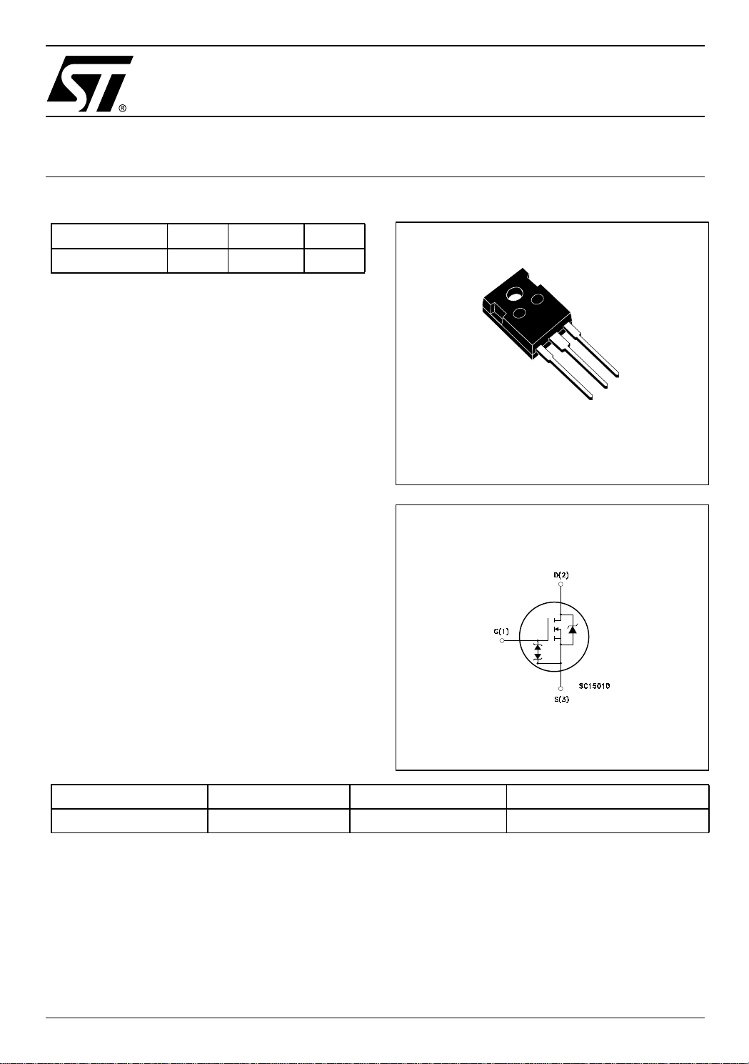
Figure 1: Package
3
2
1
TO-247
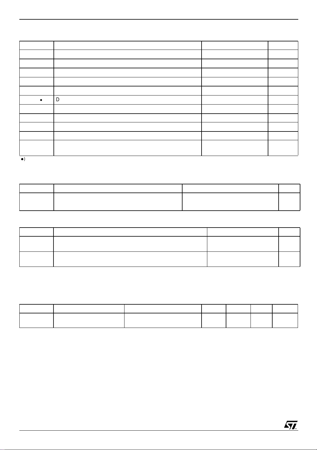
Figure 2: Internal Schematic Diagram
APPLICATIONS
The MDmesh™ family is very suitable for increasing power density of high voltage converters allowing system miniaturization and higher efficiencies.
Table 2: Order Codes
SALES TYPE MARKING PACKAGE PACKAGING
STW26NM60 W26NM60 TO-247 TUBE
Rev. 5
1/9February 2005
STW26NM60
Table 3: Absolute Maximum ratings
Symbol Parameter Value Unit
V
DS
V
DGR
V
GS
I
D
I
D
I
DM
P
TOT
V
ESD(G-S)
dv/dt (1) Peak Diode Recovery voltage slope 15 V/ns
T
j
T
stg
() Pulse width limited by saf e operating area
≤26A, di/dt ≤200A/µs, VDD ≤ V
(1) I
SD
Table 4: Thermal Data
Rthj-case Thermal Resistance Junction-case Max 0.4 °C/W
Rthj-amb Thermal Resistance Junction-ambient Max 62.5 °C/W
T
l
Drain-source Voltage (VGS = 0)
Drain-gate Voltage (RGS = 20 kΩ)
600 V
600 V
Gate- source Voltage ± 30 V
Drain Current (continuous) at TC = 25°C
Drain Current (continuous) at TC = 100°C
()
Drain Current (pulsed) 120 A
Total Dissipation at TC = 25°C
30 A
18.9 A
313 W
Derating Factor 2.5 W/°C
Gate source ESD(HBM-C=100pF, R=1.5KΩ) 6000 V
Operating Junction Temperature
Storage Temperature
, Tj ≤ T
(BR)DSS
JMAX.
-55 to 150 °C
Maximum Lead Temperature For Soldering Purpose 300
°C
Table 5: Avalanche Characteristics
Symbol Parameter Max Value Unit
I
AR
E
AS
Avalanche Current, Repetitive or Not-Repetitive
(pulse width limited by T
max)
j
Single Pulse Avalanche Energy
(starting T
= 25 °C, ID = IAR, VDD = 50 V)
j
ELECTRICAL CHARACTERISTICS (T
=25°C UNLESS OTHERWISE SPECIFIED)
CASE
13 A
740 mJ
Table 6: Gate-Source Zener Diode
Symbol Parameter Test Conditions Min. Typ. Max. Unit
BV
GSO
Gate-Source Breakdown
Igss=± 1mA (Open Drain) 30 V
Voltage
PROTECTION FEATURES OF GATE-TO-SOURCE ZENER DIODES
The built-in back-to-back Zener diodes have specifically been designed t o enhance not only t he device’s
ESD capability, but also to make them safely absorb possible voltage transients that may occasionally be
applied from gate to source. In this respect the Zener voltage is appropriate to achieve an efficient and
cost-effective intervention to p r otect the device’s integrity. These integrated Zener diodes thus avoid the
usage of external components.
2/9
STW26NM60
Table 7: On /Off
Symbol Parameter Test Conditions Min. Typ. Max. Unit
V
(BR)DSS
Drain-source Breakdown
Voltage
I
I
V
GS(th)
R
DS(on
DSS
GSS
Zero Gate Voltage
Drain Current (V
GS
= 0)
Gate-body Leaka ge
Current (V
DS
= 0)
Gate Threshold Voltage
Static Drain-source On
Resistance
Table 8: Dynamic
Symbol Parameter Test Conditions Min. Typ. Max. Unit
g
(1) Forward Transconductance VDS = 15 V , ID = 13 A 20 S
fs
C
OSS eq
C
C
C
t
d(on)
t
d(off)
Q
Q
Q
iss
oss
rss
t
r
t
f
gs
gd
g
Input Capacitance
Output Capacitance
Reverse Transfer
Capacitance
(3).Equivalent Outpu t
Capacitance
Turn-on Delay Time
Rise Time
Turn-off-Delay Time
Fall Time
Total Gate Charge
Gate-Source Charge
Gate-Drain Charge
ID = 250 µA, VGS = 0 600 V
V
= Max Rating
DS
V
= Max Rating, TC = 125°C
DS
V
= ± 20 V ± 10 µA
GS
V
= VGS, ID = 250 µA 3
DS
4
10
100
5V
VGS = 10 V, ID = 13 A 0.125 0.135 Ω
= 25 V, f = 1 MHz,
V
DS
VGS = 0
2900
900
40
VGS = 0 V, VDS = 0 to 400 V 300 pF
= 300 V, ID = 13 A,
V
DD
RG = 4.7 Ω, V
GS
(see Figure 15)
= 10 V
35
22
14
20
= 480 V, ID = 26 A,
V
DD
VGS = 10 V
(see Figure 18)
73
20
37
102 nC
µA
µA
pF
pF
pF
ns
ns
ns
ns
nC
nC
Table 9: Source Drain Diode
Symbol Parameter Test Conditions Min. Typ. Max. Unit
I
SD
I
SDM
V
(1)
SD
t
rr
Q
rr
I
RRM
t
rr
Q
rr
I
RRM
(1) Pulsed: Pulse durat ion = 300 µs, duty cycle 1.5 %.
(2) Pulse width limite d by safe operatin g area.
(3) C
oss eq.
Source-drain Current
(2)
Source-drain Current (pulsed)
Forward On Voltage
Reverse Recovery Time
Reverse Recovery Charge
Reverse Recovery Current
Reverse Recovery Time
Reverse Recovery Charge
Reverse Recovery Current
is defined as a constant equivalent capacitance giving the same charging time as C
ISD = 26 A, VGS = 0
= 26 A, di/dt = 100 A/µs
I
SD
VDD = 100V
(see Figure 16)
= 26 A, di/dt = 100 A/µs
I
SD
V
= 100V, Tj = 150°C
DD
(see Figure 16)
450
7
30.5
560
9
32.5
when VDS increase s from 0 to 80% V
oss
26
104
1.5 V
A
A
ns
µC
A
ns
µC
A
DSS
3/9
.
 Loading...