

STV7733
AOC1
DBA1
DBA2
DIR /CS SCLK VDD
/DL
VSSL
DBB1
DBB2
DBC1
DBC2
AOC2
HVDD
STBTEST
OUT1 OUT2 OUT320
MVDD
2 x 320-bit latch
Q1 Q2 Q3 Q4 Q320
Output control
Tri-level output buffer stage
DBD1
DBD2
Shift register direction
2 x 80-bit shift register
VSSP
HVDD
MVDD
VSSP
Data decoding
POE
VSSS
2 x 80-bit shift register
2 x 80-bit shift register
2 x 80-bit shift register
OE
320 output dot-matrix display driver
Preliminary Data
Features
■
High-voltage, row/column driver IC
■
320, tri-level (high-voltage, medium voltage
and ground) power outputs:
– capable of operating at 90V, absolute max.
– capable of sinking or sourcing 2mA
– Hi-Z
■
Logic supply range: 2.5V to 3.3V
■
Slim shape die for COG, COF and TCP
solutions
■
Interface:
– four dual (2-bit) input serial buses:
DBA[1:2], DBB[1:2], DBC[1:2] and DBD[1:2]
operating at shift clock frequency of
10MHz, max.
– three control inputs: shift clock direction
(DIR), chip select (/CS) and data latch
(/DL)
– two “all output” stage control inputs: AOC1
and AOC2
■
Power supplies:
– high-voltage for power outputs: 90V, max.
– logic supply suitable for battery powered
applications: 2.5V, min.
The STV7733 communicates with the host
controller through an 8-bit parallel interface. The
input data bus is organized as four, 2 x 80-bit shift
registers operating in parallel at a maximum clock
frequency of 10MHz.
Logic inputs are LVCMOS compatible.
The STV7733 is available in bumped die form.
Bumped die can be assembled in either a TCP or
COG module.
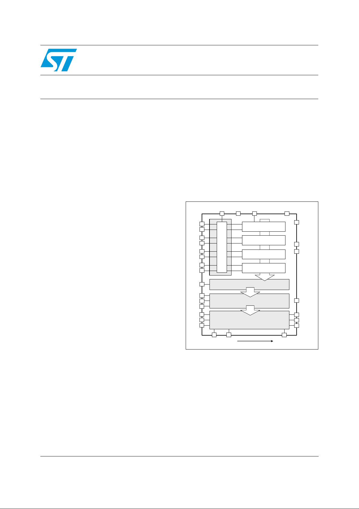
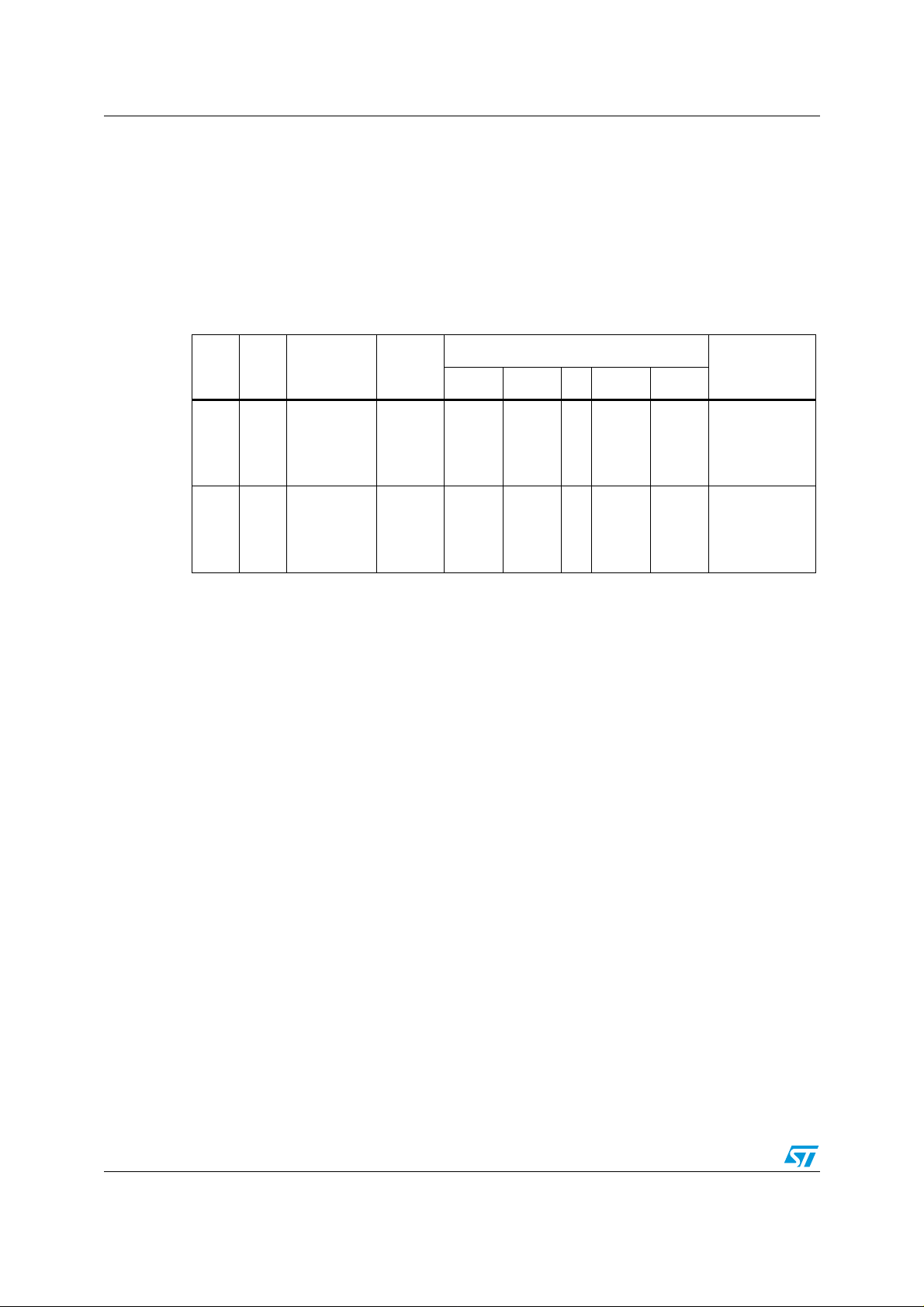
Figure 1. Block diagram
Description
The STV7733 device is a low-power,
controller/driver IC for dot-matrix displays. Data is
encoded on two bits to select one of four possible
output states: high level, medium level, ground or
high impedance (Hi-Z).
Inputs AOC1 and AOC2 control the all output
stages simultaneously to select one of five
possible configurations: high level, medium level,
ground, Hi-Z or data through.
Except for the data through mode, the
configuration selected by AOC1 and AOC2 is
applied to all outputs at the same time.
May 2007 Rev 1 1/28
This is preliminary information on a new product now in development or undergoing evaluation. Details are subject to
change without notice.
www.st.com
28

Contents STV7733
Contents
1 Block diagram . . . . . . . . . . . . . . . . . . . . . . . . . . . . . . . . . . . . . . . . . . . . . . 3
2 Pin description . . . . . . . . . . . . . . . . . . . . . . . . . . . . . . . . . . . . . . . . . . . . . 4
3 Die pinout . . . . . . . . . . . . . . . . . . . . . . . . . . . . . . . . . . . . . . . . . . . . . . . . . . 5
4 Data bus configuration . . . . . . . . . . . . . . . . . . . . . . . . . . . . . . . . . . . . . . . 6
5 Power output stage . . . . . . . . . . . . . . . . . . . . . . . . . . . . . . . . . . . . . . . . . . 7
6 Absolute maximum ratings . . . . . . . . . . . . . . . . . . . . . . . . . . . . . . . . . . . 8
7 Electrical characteristics . . . . . . . . . . . . . . . . . . . . . . . . . . . . . . . . . . . . . 9
8 AC timing requirements . . . . . . . . . . . . . . . . . . . . . . . . . . . . . . . . . . . . . 11
9 AC Timing characteristics . . . . . . . . . . . . . . . . . . . . . . . . . . . . . . . . . . . 12
10 Timing . . . . . . . . . . . . . . . . . . . . . . . . . . . . . . . . . . . . . . . . . . . . . . . . . . . . 13
11 Pad dimensions (in microns)/pad positions . . . . . . . . . . . . . . . . . . . . 14
12 Ordering information . . . . . . . . . . . . . . . . . . . . . . . . . . . . . . . . . . . . . . . 27
13 Revision history . . . . . . . . . . . . . . . . . . . . . . . . . . . . . . . . . . . . . . . . . . . 27
2/28
STV7733 Block diagram
AOC1
DBA1
DBA2
DIR /CS SCLK VDD
/DL
VSSL
DBB1
DBB2
DBC1
DBC2
AOC2
HVDD
STBTEST
OUT1 OUT2 OUT320
MVDD
2 x 320-bit latch
Q1 Q2 Q3 Q4 Q320
Output control
Tri-level output buffer stage
DBD1
DBD2
Shift register direction
2 x 80-bit shift register
VSSP
HVDD
MVDD
VSSP
Data decoding
POE
VSSS
2 x 80-bit shift register
2 x 80-bit shift register
2 x 80-bit shift register
OE
1 Block diagram
Figure 2. STV7733 block diagram
3/28
Pin description STV7733
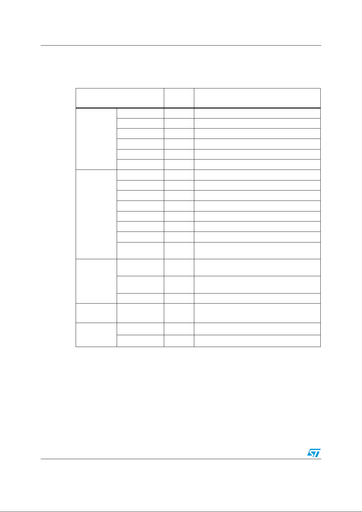
2 Pin description
Table 1. STV7733 pin description
Pin name
Power
supplies
Input logic
block
Power output
control
Pin type
(I/O)
HVDD I Output buffer - high-voltage supply
MVDD I Output buffer - medium voltage supply
VSSP I Output buffer - ground level
VDD I Logic power supply
VSSL I Logic ground
VSSS I Chip substrate level
DBA[1:2] I Input data bus, 2-bit serial interface
DBB[1:2] I Input data bus, 2-bit serial interface
DBC[1:2] I Input data bus, 2-bit serial interface
DBD[1:2] I Input data bus, 2-bit serial interface
SCLK I Data shift clock
DIR I Shift clock direction
/CS I Chip select (0 = select, 1 = un-select)
/DL I
AOC1 I
AOC2 I
POE I Power output enable
Data latch. Shift register data is transferred to the
driver outputs at the falling edge of this pulse.
“All-output” control (all HVDD, all MVDD, all VSSP,
data through mode) selection pin
“All-output” control (all HVDD, all MVDD, all VSSP,
data through mode) selection pin
Pin description
Power
outputs
Test
4/28
OUT1to OUT320 O High-voltage power outputs
STBTEST I Must be grounded
OE I Must be grounded
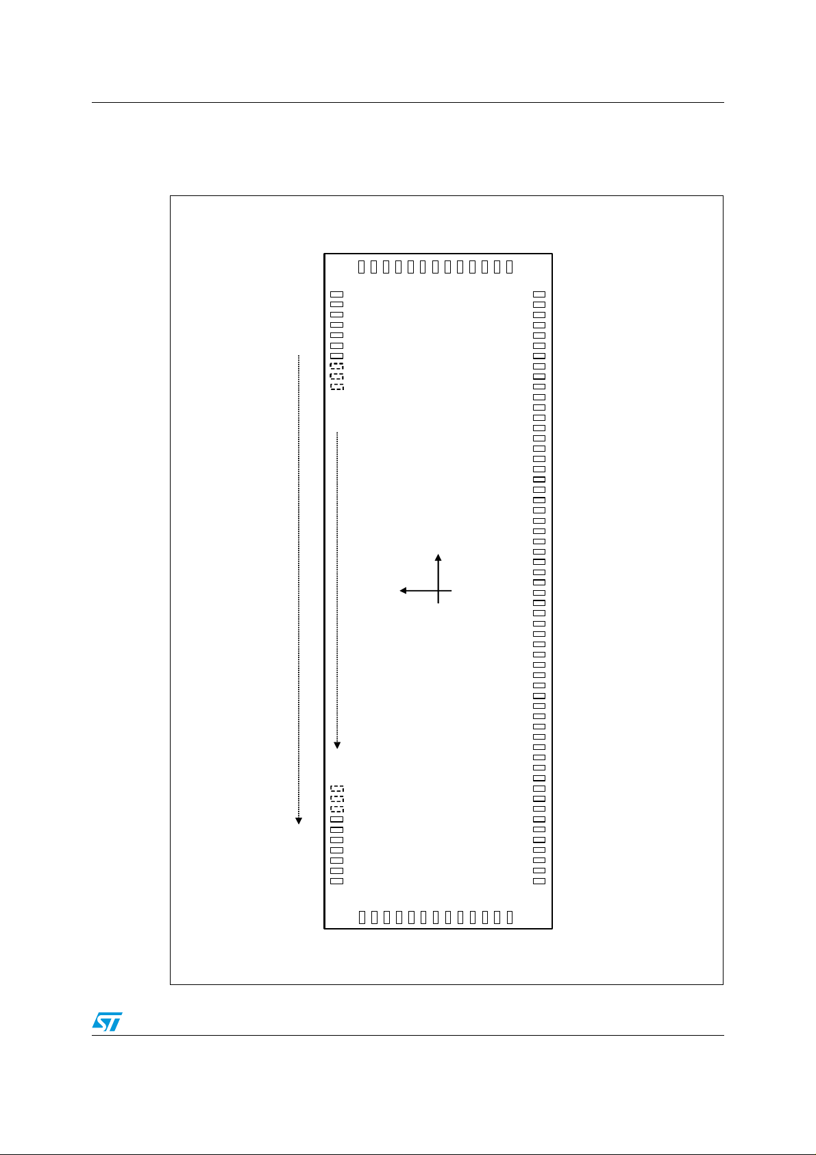
STV7733 Die pinout
Y
X
0/0
DUMMY
DUMMY
DUMMY
DUMMY
DUMMY
DUMMY
DUMMY
DUMMY
DUMMY
DUMMY
DUMMY
VDD
VSSS
VSSL
OE
DBD2
DBD1
DBC2
DBC1
DUMMY
DUMMY
DUMMY
DUMMY
DBB2
DBB1
DBA2
DBA1
VDD
VSSS
VSSL
CS
SCLK
DL
VSSL
VSSS
VDD
AOC2
AOC1
DUMMY
DUMMY
POE
DIR
STBTEST
VSSL
VSSS
VDD
DUMMY
DUMMY
DUMMY
DUMMY
DUMMY
DUMMY
DUMMY
DUMMY
DUMMY
DUMMY
DUMMY
DUMMY
OUT1
OUT2
OUT3
OUT4
OUT5
OUT316
OUT317
OUT318
OUT319
OUT320
VSSP
VSSP
HVDD
HVDD
MVDD
MVDD
VSSL
VSSS
VDD
DUMMY
DUMMY
DUMMY
DUMMY
VSSP
VSSP
HVDD
HVDD
MVDD
MVDD
VSSL
VSSS
VDD
DUMMY
DUMMY
DUMMY
DUMMY
3 Die pinout
Figure 3. Die pinout
5/28
Data bus configuration STV7733
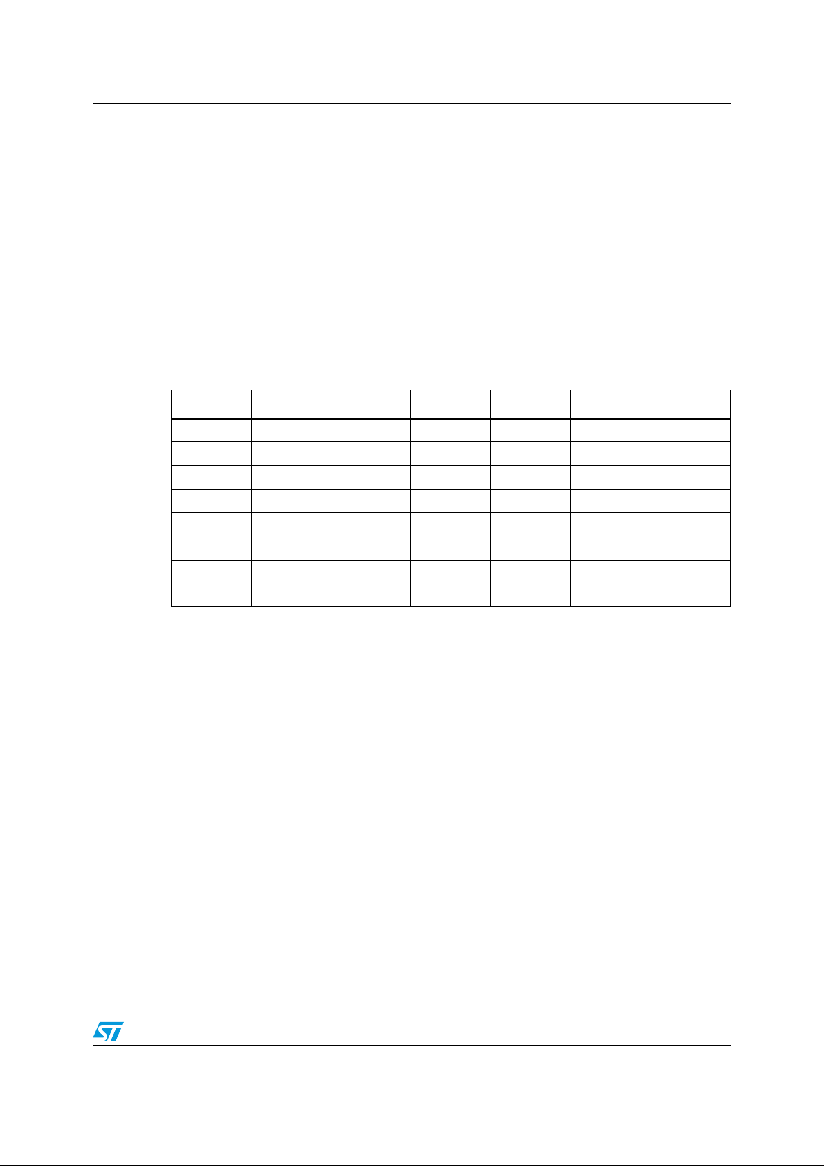
4 Data bus configuration
Below, Table 2 describes the position of the first data sampled by the first rising edge of the
SCLK clock. For the first configuration described in Table 2, that is, with input DIR = “H”,
data on the 2-bit bus DBA is sampled by the first SCLK clock pulse and appears on power
output OUT1. After 80 clock pulses, data on OUT1 will be shifted to OUT317 - on the
high-to-low transition of input /DL. Input /CS is the chip select.
Table 2. Data bus configuration
SCLK pulse number
/CS DIR Input Position
OUT1 OUT2 … OUT79 OUT80
Comment
L H
L L
DBA[1:2]
DBB[1:2]
DBC[1:2]
DBD[1:2]
DBA[1:2]
DBB[1:2]
DBC[1:2]
DBD[1:2]
OUT
OUT
OUT
OUT
OUT
OUT
OUT
OUT
01
02
03
04
320
319
318
317
05
06
07
08
316
315
314
313
313
314
315
316
08
07
06
05
317
318
319
320
04
03
02
01
Left/Right shift
Right/Left shift
Note: Data is transferred from the shift register to a latch block and then on to power output stages
on the falling edge of input /DL, see Figure 2.
All output data is stored and held in the latch block on the rising edge of the input /DL, see
Figure 2.
6/28
STV7733 Power output stage
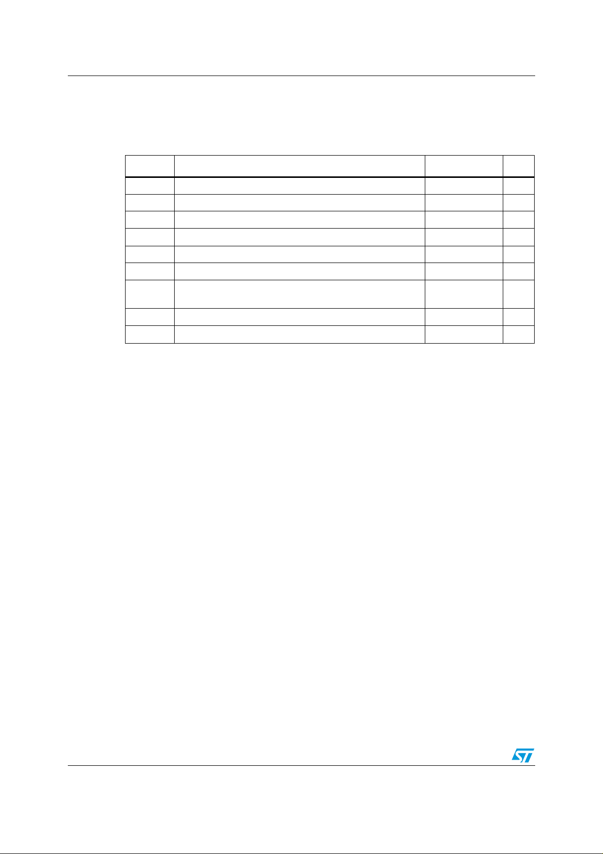
5 Power output stage
The power output stage is defined by a set of three switches that can select three different
output voltages (HVDD, MVDD or V
the output stage in a high impedance (Hi-Z) mode.
Depending on the configuration of logic inputs AOC1 and AOC2, the power output stage is
configured in either a “data through” mode or a “simultaneous” mode. In the “data through”
mode (for AOC1 = AOC2 = “L”), the power output stage converts the 2-bit encoded data that
was loaded into the latch stage for each column into a high-voltage level that appears on the
output pin. When AOC1 and AOC2 are not both “L”, the power outputs can all operate
simultaneously - going to V
, MVDD or HVDD depending on AOC1 and AOC2 as described
SSP
below in Table 3.
Table 3. Power output truth table
DBn[1] DBn[2] POE AOC1 AOC2 OUTn Comment
X X L X X All Hi-Z
L L H L L Hi-Z
H L H L L V
H H H L L MV
L H H L L HV
X X H H L All V
X X H L H All MV
X X H H H All HV
1. With input POE = “L”, all power outputs are not active, that is, they are all in Hi-Z.
2. Data through mode: each power output depends on the DBn[1:2] value at the falling edge of input /DL.
3. Output simultaneous mode: all power outputs depend on the “H”/”L” input values for AOC1 and AOC2.
). These switches can also be all opened to configure
SSP
SSP
DD
DD
SSP
DD
DD
(1)
(2)
(2)
(2)
(2)
(3)
(3)
(3)
7/28
Absolute maximum ratings STV7733
6 Absolute maximum ratings
Table 4. Absolute maximum ratings
Symbol Parameter Value Units
V
HV
MV
V
I
POUT
V
OUT
V
ESD
Logic supply range -0.3, +7 V
DD
Driver supply range -0.3, +90 V
DD
Driver supply range -0.3, +HVdd -10 V
DD
Logic input voltage range -0.3, VDD+0.3 V
IN
Driver output current ±5 mA
Power output voltage range -0.3, +90 V
ESD susceptibility, Human Body model
(100pF discharged through 1.5kohms)
2.0 kV
Tjmax Maximum junction temperature 100 °C
Tstg Storage temperature range -50, +150 °C
8/28
STV7733 Electrical characteristics
7 Electrical characteristics
VDD = 3V, HVDD = 70V, MVDD = 35V, V
SSP
= 0V, V
SSL
= 0V, V
SSS
= 0V, T
amb
= 25°C,
F = 10MHz, unless otherwise specified.
Table 5. Electrical characteristics
Symbol Parameter Min. Typ. Max. Units
Supply
V
I
I
DD1
I
DD2
HV
MV
I
OUT1 to OUT320
V
HPOUTH
V
MPOUTH
V
POUTL
I
POUTH
VDD supply voltage 2.5 3 3.3 V
DD
VDD supply current with no clock, all logic inputs set to either
DD
0V or VDD and all power outputs in Hi-Z
- - 0.5 µA
VDD dynamic supply current @ clock frequency = 5MHz
(data frequency is 2.5MHz)
VDD dynamic supply current @ clock frequency = 100kHz
(data frequency = 50kHz
HVDD supply voltage 15 80 V
DD
MVDD supply voltage
DD
HVDD supply current in steady state - - 10 µA
PP
(1)
(2)
- 3 - mA
- 0.1 - mA
15 70 V
Power output high level (voltage difference versus HVDD)
@ I
HPOUTH
= -0.5mA and HV
= 80V - - -10 V
DD
Power output medium level (voltage difference versus
MVDD)
@ I
MPOUTH
@ I
MPOUTL
= + 0.5mA and MV
= - 0.5mA and MV
DD
DD
= 40V
= 40V
-
-
--+10
Power output low level
@ I
= + 0.5mA - - +10 V
POUTL
Output current from HVDD, MVDD (see Figure 4)
1) HVDD = 80V, MVDD = 40V
2) HVDD = 60V, MVDD = 30V
-1.42
-0.7
-10
- mA
V
V
mA
I
POUTM
I
POUTL
I
HiZ
Output current from output to MVDD (Figure 4)
1) HVDD = 80V and MVDD = 40V
2) HVDD = 60V and MVDD = 30V
Output current from output to V
@ Vdd=2.5V (Figure 4)
SSP
1) HVDD = 80V and MVDD = 40V
Output current during Hi-Z mode
@ V
= 2.5V, HVDD = 80V and MVDD = 40V
DD
9/28
+1.5
+0.7
mA
mA
+1.5 - mA
- 10 µA
 Loading...