

Features
■ 2-level high voltage output gate driver
■ 480 channels with -40/+35 mA source/sink
output current capability
■ 75 V output swing within +/- 45 V limits
■ 3.0 to 3.6 V digital power supply
■ 1.8 V CMOS input signal compatibility
■ Selectable 480 or 400 outputs
■ Direct input to bidirectional shift registers
■ Selectable polarity and blanking function
■ High voltage BCD process technology
■ Bumped dice in tray
■ Output stage similar to STV7622
■ PCB-less compatible dice
STV7623
480 output high-voltage gate driver
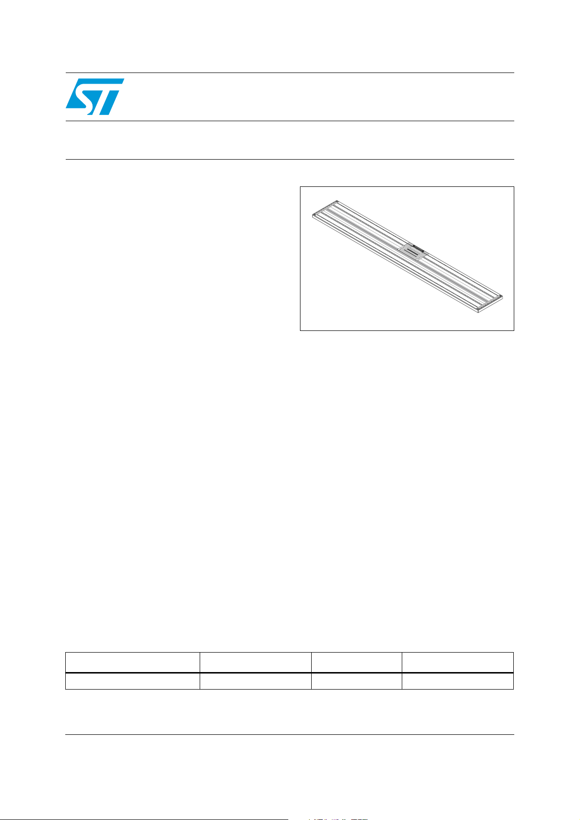
STV7623 die
Description
The STV7623 is a 1-bit x 480 shift register with
dual rail high voltage/medium current output, with
global blank and polarity control.
Table 1. Device summary
Order code Temperature Package Packing
STV7623WPB3 -25
The maximum shift frequency starts from 1 MHz
for a 1.8 V type input signal, up to 10 MHz for a
3.3 V type input signal. This generic device can
be used for segmented/dot matrix
electroluminescent displays to drive an array of
organic electronic transistors, or for technologies
related to e-Paper/e-Reader/digital signage
solutions.
The device can be daisy-chained for various
display resolutions.
°C to +70°C Bumped dice 3-inch tray
August 2011 Doc ID 018939 Rev 1 1/27
www.st.com
27

Contents STV7623
Contents
1 Description . . . . . . . . . . . . . . . . . . . . . . . . . . . . . . . . . . . . . . . . . . . . . . . . . 3
1.1 Pin description . . . . . . . . . . . . . . . . . . . . . . . . . . . . . . . . . . . . . . . . . . . . . . 4
2 Functional description . . . . . . . . . . . . . . . . . . . . . . . . . . . . . . . . . . . . . . . 6
2.1 Device operation . . . . . . . . . . . . . . . . . . . . . . . . . . . . . . . . . . . . . . . . . . . . 6
2.2 Device power supply . . . . . . . . . . . . . . . . . . . . . . . . . . . . . . . . . . . . . . . . . 7
2.3 Power sequencing . . . . . . . . . . . . . . . . . . . . . . . . . . . . . . . . . . . . . . . . . . . 7
3 Truth tables . . . . . . . . . . . . . . . . . . . . . . . . . . . . . . . . . . . . . . . . . . . . . . . . 9
4 Absolute maximum rating . . . . . . . . . . . . . . . . . . . . . . . . . . . . . . . . . . . 10
5 Electrical characteristics . . . . . . . . . . . . . . . . . . . . . . . . . . . . . . . . . . . . 11
5.1 DC electrical characteristics (DGND = 0 V) . . . . . . . . . . . . . . . . . . . . . . . 11
5.2 AC characteristics . . . . . . . . . . . . . . . . . . . . . . . . . . . . . . . . . . . . . . . . . . 13
5.3 Timing requirements . . . . . . . . . . . . . . . . . . . . . . . . . . . . . . . . . . . . . . . . . 14
6 Packing information . . . . . . . . . . . . . . . . . . . . . . . . . . . . . . . . . . . . . . . . 15
7 Pad information . . . . . . . . . . . . . . . . . . . . . . . . . . . . . . . . . . . . . . . . . . . . 18
8 Revision history . . . . . . . . . . . . . . . . . . . . . . . . . . . . . . . . . . . . . . . . . . . 26
2/27 Doc ID 018939 Rev 1

STV7623 Description
^ ^ ^ ^ ^ ^ ^ ^
B LA NK
48 0 bi ts bi - dir ec tion al sh ift r eg ist er
S TV 1
S TV 2
C LK
D IR
V P
V N
LE N GTH
TE ST
JU ST IFY
1 Description
Figure 1. STV7623 block diagram
OUT1 OUT2 OUT3 OUT4
POL
OUT477 OUT478 OUT 479 OUT480
Level Shifter
DVDD
DGND
AM08731V1
Doc ID 018939 Rev 1 3/27

Description STV7623
1.1 Pin description
Figure 2. PCB-Less COF pinout diagram
Test20
Test20
Test19
Test18
Test17
Test16
Test15
Test14
Test13
Test12
Test11
OUT480
VP
DVDD
DGND
VN
STV2
TEST
DIR
CLK
BLANK
POL
BLANK
CLK
DIR
LENGTH
STV1
VN
DGND
DVDD
VP
0UT1
Test10
Test9
Test8
Test7
Test6
Test5
Test4
Test3
Test2
Test1
Test20
Test19
Test19
Test18
Test18
Test17
Test17
Test16
Test16
Test15
Test15
Test14
Test14
Test13
Test13
Test12
Test12
Test11
Test11
OUT480
VP
DVDD
DGND
VN
STV2
TEST
DIR
DVDD
CLK
BLANK
POL
DGND
POL
BLANK
CLK
JUSTIFY
DIR
LENGTH
STV1
VN
DGND
DVDD
VP
0UT1
Test10
Test10
Test9
Test9
Test8
Test8
Test7
Test7
Test6
Test6
Test5
Test5
Test4
Test4
Test3
Test3
Test2
Test2
Test1
Test1
Test20
Test20
Test19
Test19
Test18
Test18
Test17
Test17
Test16
Test16
Test15
Test15
Test14
Test14
Test13
Test13
Test12
Test12
Test11
Test11
Out480
Out480
Out479
Out479
Out478
Out478
Out477
Out477
-
-
-
-
-
-
-
-
-
-
-
-
-
-
-
-
-
-
-
-
-
-
-
-
Out4
Out4
Out3
Out3
Out2
Out2
Out1
Out1
Test10
Test10
Test9
Test9
Test8
Test8
Test7
Test7
Test6
Test6
Test5
Test5
Test4
Test4
Test3
Test3
Test2
Test2
Test1
Test1
Figure 2 shows the possible design of a custom COF with wire on array (WOA) routing
(PCB-less). This example supports only 480 outputs.
Table 2. Pin description
Pin name I/O Function Description
CLK In Shift clock Input
DIR In
STV1
STV2
BLANK In
I/O
Shift direction
Control pin
Start pulse
input/output pin
Output enable
control
4/27 Doc ID 018939 Rev 1
Clock input for the chip internal shift register. Data
is shifted at each rising edge of this clock.
This pin controls the output shifting direction.
These pins are used to control the channel start
pulse input or output pin. The function of these
two pins depends on the status of DIR pin (refer
to the Section 3: Truth tables)
This pin is used to control the channel output.
When BLANK is high, the shift register is
bypassed (overriden) and all driver outputs are
fixed to VN level instantly, (when POL= L).
It is assumed this signal affect few outputs
STV7623 Description
Table 2. Pin description (continued)
Pin name I/O Function Description
When POL is low, VP and VN are swapped
POL In Polarity pin
OUT1..OUT480 Out Driver output pins
VP Power Power supply High voltage supply (eg +50 V)
DVDD Power Power supply Digital power supply
DGND Power Power supply Digital ground
VN Power Power supply Negative supply
TEST In Test pin Test pin (must be grounded in application)
functionally at the output pins level.
This signal is assumed static.
The output voltage is either VP or VN for driving
the gate electrode, depending on the data stored
in the shift register. It is assumed that only up to 4
outputs are changing level simultaneously.
LENGTH In
JUSTIFY In
Nb of active
outputs
Partial output
justify mode
In the pinout diagram:
● TEST is used to test the device.
When LENGTH =0, enable 480 outputs
When LENGTH =1, enable 400 outputs
This signal is assumed static
Only applicable when LENGTH=1
When JUSTIFY = 0, use outputs 0 to 399
When JUSTIFY = 1, use outputs 80 to 479
This signal is assumed static.
Doc ID 018939 Rev 1 5/27
Functional description STV7623
2 Functional description
The STV7623 includes all the logic and power circuits necessary to drive the thin-film
transistor (TFT) of an active matrix display backplane. A low-voltage logic block manages
data information, and a high-voltage block converts the low-voltage information stored in the
logic block into high-voltage signals applied to the display gate lines.
2.1 Device operation
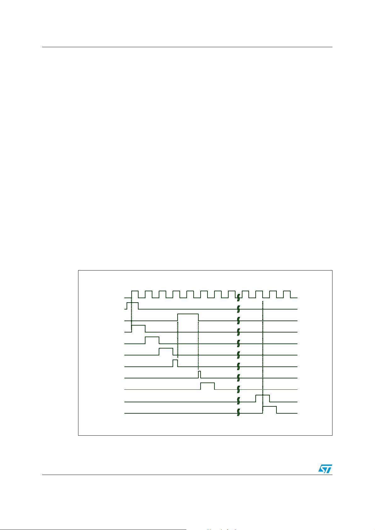
In the condition of DIR=L, the STV1 start pulse input is sensed at the rising edge of CLK and
stored in the first stage of shift register, which causes the first scan signal is outputted from
the OUT1 output pin. While stored data is transferred to the next stage of the shift register at
the rising edge of the CLK signal, new data of STV1 is sensed and stored simultaneously.
The output pin (OUT1 to OUT480) supplies VP or VN voltage to the gate lines depending on
the data stored in the shift register. For normal operation, a VP voltage is outputted one by
one like a shift token from OUT1 to OUT480, in sync with CLK pulse.
STV2 goes up to high level at the 400/480th falling edge of CLK and goes down to low level
at the 401/481th falling edge of CLK. This STV2 is connected to the next driver IC STV1
signal to cascade (daisy chain) them.
When STV2 is an output, the signal is activated for 1/2 clock later.
When the chip is configured in 400 output mode, only the first 400 bits entering the shift
register are used, the remaining 80 outputs are removed from the shift register.
Figure 3. Example of input/output timing DIR = H
Example of input/output timing (DIR=0)
1 2 3 4 5 6 7 479 480 481 482
CLK
STV1
BLANK
OUT1
OUT2
OUT3
OUT4
OUT5
OUT6
OUT480
STV2
6/27 Doc ID 018939 Rev 1
STV7623 Functional description
2.2 Device power supply
The STV7623 must be used with the following conditions when operating:
– VP - VN < 75 V
– VP-DGND > 10 V
–DGND-VN>10V
Figure 4. Device power supply
Output 1 to 480
VP
DVD D
DGND
VN
2.3 Power sequencing
To prevent the device from being damaged by latchup, the power ON/OFF sequence it is
recommended to follow the procedure below:
– Power OFF => ON: DVDD -> VN -> VP
– Power ON => OFF, VP -> VN -> DVDD
Logic input
AM08733V1
Doc ID 018939 Rev 1 7/27
Functional description STV7623
Figure 5. Power sequencing
VP
DVDD
DGND
VN
AM08734V1
8/27 Doc ID 018939 Rev 1

STV7623 Truth tables
3 Truth tables
Table 3. Output level truth table
Input pins
Data bit Blank POL OUTn
001 VP (+)
101 VN (-)
X 1 1 VP (+)
X 1 0 VN (-)
100 VP (+)
000 VN (-)
Table 4. Output ordering truth table
Configurations
Comments
Length Justify Dir In First Last Out
0 0 0 STV1 OUT1 OUT480 STV2 All outputs
0 1 0 STV1 OUT1 OUT480 STV2 All outputs
1 0 0 STV1 OUT1 OUT400 STV2 1..400
1 1 0 STV1 OUT81 OUT480 STV2 81..480
0 0 1 STV2 OUT480 OUT1 STV1 All outputs
0 1 1 STV2 OUT480 OUT1 STV1 All outputs
1 0 1 STV2 OUT400 OUT1 STV1 1..400
1 1 1 STV2 OUT480 OUT81 STV1 81..480
When only 400 outputs are used, the remaining 80 outputs remain static.
Doc ID 018939 Rev 1 9/27

Absolute maximum rating STV7623
4 Absolute maximum rating
Stressing the device above the rating listed in the “absolute maximum ratings” table may
cause permanent damage to the device. These are stress ratings only and operation of the
device at these or any other conditions above those indicated in the operating sections of
this specification is not implied. Exposure to absolute maximum rating conditions for
extended periods may affect device reliability.
Table 5. Absolute maximum ratings (V
=0V, 25°C)
SS
Symbol Parameter Value Unit
V
DD
Digital supply range -0.3 to +4.0 V
VP Positive voltage supply -0.3 to +50 V
VN Negative voltage supply +0.3 to -50 V
Vp-Vn Voltage difference 90 V
V
I
pout
I
dout
V
out
Logic input voltage range -0.3 to DVDD+0.3 mV
IN
Driver output current x
Diode output current
(1) (2) (3)
(1) (2) (3)
- 70 to +35 mA
-200 to +300 mA
Output voltage range -0.3 to +90 V
ESD susceptibility, human body model (100 pF
V
ESD
discharged through 1.5 KΩ), on all except the V
CC
2kV
pins(4)
T
jmax
T
stg
1. Measurements done on one single output, x. The other outputs are either not used or are connected to
output x. Assumes junction temperature remains less than Tjmax during measurement.
2. All transient current measurements are made under conditions close to those encountered in a typical
application (that is, with duration of any output current spike always less than 300 ns).
3. These parameters are measured during STMicroelectronics’ internal qualification which includes
temperature characterization on standard as well as corner batches of the process. These parameters are
not tested in production.
Maximum junction temperature -40 to +100 °C
Storage temperature range (die) -65 to +150 °C
10/27 Doc ID 018939 Rev 1

STV7623 Electrical characteristics
5 Electrical characteristics
5.1 DC electrical characteristics (D
D
= 3.3 V, VP = 30 V, VN = -45V, T
VDD
Table 6. Electrical characteristics - supply
Symbol Parameter
D
VDD
I
DD
I
DDL
I
DD
V
P
V
N
V
P-VN
I
PPH
1. For 3.3V CMOS input logic levels (0 or 3.3 V)
2. All input data is switched at 0.5 MHz rate.
Digital supply voltage 3.0 3.3 3.6 V
Digital supply current
(1)
Digital dynamic supply
current (CLK1 freq =
(2)
1MHz)
Digital supply current at
V
= 2.0 V
IH
DC power output positive
supply voltage
DC power output negative
supply voltage
Voltage gap Vp-Vn 20 – 80 V
Power output supply current
(steady outputs)
AMB
= 25 °C, f
=0V)
GND
= 1 MHz, unless otherwise specified.
CLK
Val ue
Unit
Min Typ Max
–60– µA
–900– µA
–80– µA
+10 – – V
––-10V
––500µA
Table 7. Electrical characteristics -
Symbol Parameter
Power output high level
Vpouth
Vpoutl
Vdouth
Vdoutl
(voltage drop versus VP)
at Ipouth = -20 mA and VP =
30 V
Power output low level at Ipoutl
= +20 mA
, VN=-45 V
Output upper diode voltage
drop at Idouth = +30 mA
Output lower diode voltage
drop at Idoutl = -30 mA
Doc ID 018939 Rev 1 11/27
OUT1 to OUT480
Val ue
Unit
Min Typ Max
–4–V
–6–V
–12V
-2 -1 – V

Electrical characteristics STV7623
Table 8. Electrical characteristics - standard mode,
TTL/LVCMOS inputs: CLK, DIR, blank, POL, STV1, STV2, length, justify
Val ue
Symbol Parameter
Min Typ Max
Unit
V
IH
V
IL
V
OH
V
OL
I
IH
I
IL
High level input voltage 1.2 – D
Low level input voltage D
High level output voltage
IOH=200µA
Low level output voltage
IOH= 200 µA
High level input current
(V
≥ 2.0 V)
IH
Low level input current
= 0 V)
(V
IL
Figure 6. Output test configuration
VP
933
21
2))
9GRXWK
,GRXWK
287Q
VDD
GND
D
-0.3 – DVdd V
VDD
D
GND
–0.6 V
–D
+0.3 V
GND
-1 – 1 µA
-1 – 1 µA
VP
933
2))
21
9GRXWO
287Q
,GRXWO
V
966396668%
VN
2XWSXWVLQNLQJFXUUHQWLV
FRQVLGHUHGDVSRVLWLYH
12/27 Doc ID 018939 Rev 1
966396668%
VN
2XWSXWVRXUFLQJFXUUHQWLV
FRQVLGHUHGDVQHJDWLYH
!-6

STV7623 Electrical characteristics
Figure 7. Supply voltage (VP,VN) setting examples
VP
VP
VP
VN
VN
5.2 AC characteristics
D
= 3.3 V to 3.6 V, T
VDD
(tr, tf) = 3 ns load condition: 68 pF, 3.9 kΩ, 333 pF.
Table 9. AC timing requirements
Symbol Parameter
amb
VP
VP
VP > 10V
0V = DGND
VN < -10V
VN
VP-VN < 80V
VN
VP > 10V
VN < -10V
VN
= -20°C to +85°C, input signal edge maximum rise and fall times
Val ue
Unit
Min Typ Max
Data clock period 0.1 – – µs
t
CLK
F
CLK
t
WHCLK
t
WLCLK
t
SDAT
t
HDAT
1. If the digital inputs are 3.3V +/-10%, max clock frequency can be 10 MHz
2. Output blanked during data shift.
Test condition: 25 °C ambient, VP = +30, VN = -45 V, D
Max clock frequency – 200k 1M/10M
Duration of clock pulse at
high level
Duration of clock pulse at
low level
Input data set-up time before
low-to-high clock transition
Input data hold-time after
low-to-high clock transition
(2)
400, 40
(2)
400, 40
25 – – ns
25 – – ns
=3.3V.
VDD
Doc ID 018939 Rev 1 13/27
(1)(2)
Hz
––ns
––ns

Electrical characteristics STV7623
5.3 Timing requirements
D
= 3.3 V, VP = +30 V, VN = -45 V, T
VDD
V
= 0.8 × D
IHmin
VDD
Table 10. AC timing characteristics
Symbol Parameter
Delay of power output change
t
PHL1
t
PLH1
t
PHL2
t
PLH2
t
PHL3
t
PLH3
after CLK transition
- High to low
- Low to high
Delay of power output change
after POL transition
- High to low
- Low to high
Delay of power output change
after BLANK transition
- High to low
- Low to high
= 25 °C, F
amb
= 1 MHz, V
clk
ILmax
= 0.2 × D
VDD
,
Val ue
Unit
Min Typ Max
–100–ns
–100–ns
–100–ns
14/27 Doc ID 018939 Rev 1

STV7623 Packing information
6 Packing information
Figure 8. Tray (top view)
("1.4.%
Doc ID 018939 Rev 1 15/27

Packing information STV7623
Figure 9. Tray (bottom view)
16/27 Doc ID 018939 Rev 1
("1.4.%

STV7623 Packing information
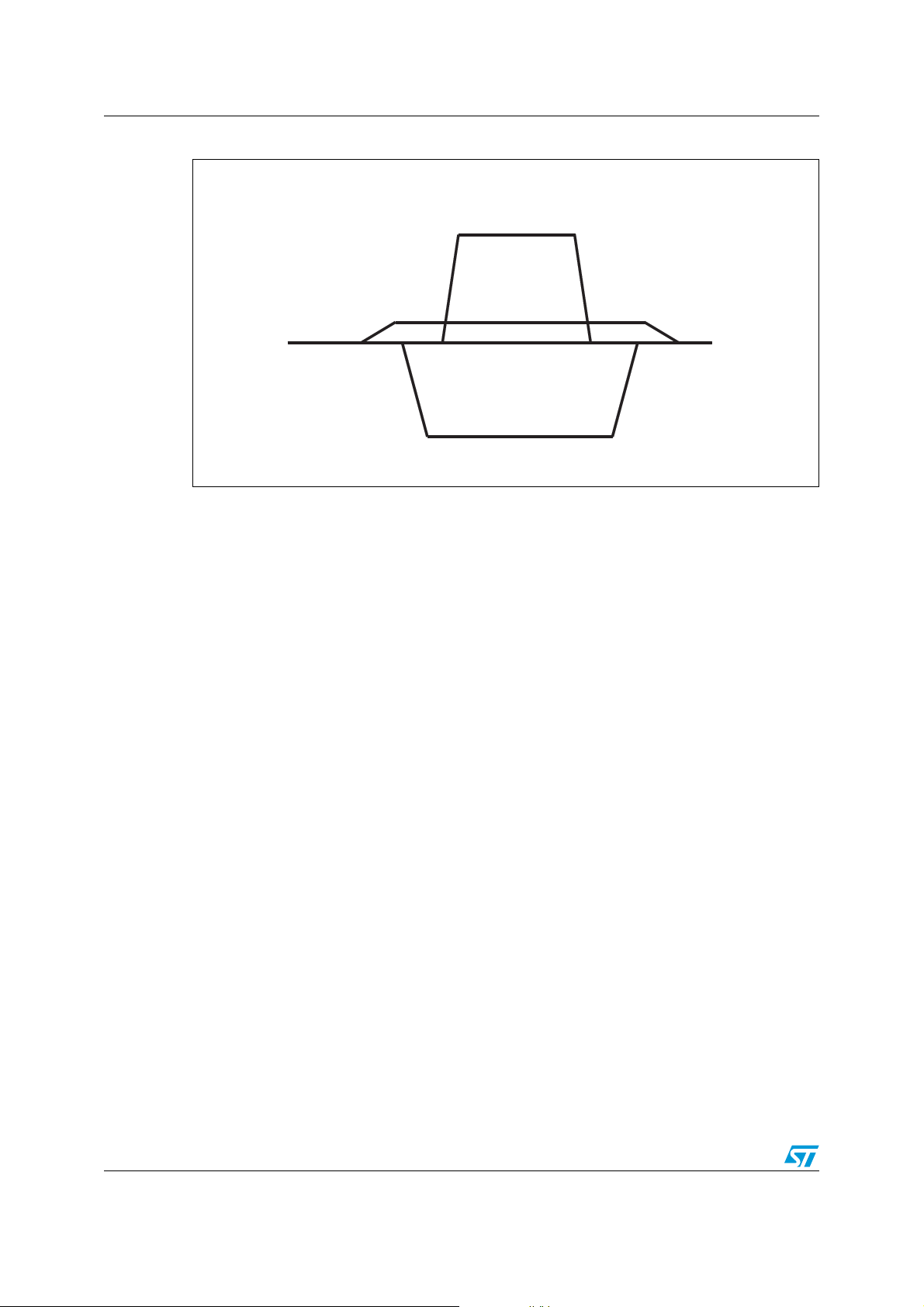
Figure 10. Die orientation in tray
DIE IDENTIFICATION
Doc ID 018939 Rev 1 17/27

Pad information STV7623
D
D
D
7 Pad information
Figure 11. Pad dimensions and coordinates (in µm)
OUT368
VP
DVDD
DGN
VN
DGN
VN
DGN
DVDD
VP
VP
DVDD
DGND
OUT480
OUT369
VP
DVDD
DGND
VN
DGND
VN
DGND
DVDD
VP
OUT113
Y
DIE FACE UP
X
(0,0)
VN
DIR
VPP
OUT1
OUT112
STV1
DVDD
DGND
CLK
POL
BLANK
JUS TIFY
LENG TH
CLK
POL
DGND
DVDD
BLANK
VN
DIR
STV2
TEST
The reference (x=0, y=0) is the centre of the die. Output pad pitch is 68 µm.
Stress relief pads are connected to V
(VSS).
N
Pad size:
● Type 1: (north/south pads) 51 x 51 µm, 68 µm linear pitch, passivation opening 34 x 34
µm.
● Type 2: (east/west) pads
● Type 3: stress relief die corner pads
Alignment: 2 alignment marks, using 2 metals across the input long edge of the die.
Die size = 51 mm
18/27 Doc ID 018939 Rev 1
2
, with special reticle/wafer map adjustments.

STV7623 Pad information
*************************
* *
* PADS extraction *
* *
*************************
release 1.4
Mon Mar 01 18:49:21 SGT 2010
CHIP NAME: STV7623_Top_ICPack
All dimensions are in Microns.
Pad Placement values correspond to each pad center coordinates.
Pad Placement Origin is the center of the die.
LEAD PAD NAME PAD PLACEMENTS PAD DIMENSIONS
X = Y = X = Y =
Note: vss! == VN line
vss! -8803.79 1251.455 73.1 73.1 (stress relief bump)
OUT<113> -8670.0 1145.46 51.0 51.0
OUT<114> -8602.0 1145.46 51.0 51.0
OUT<115> -8534.0 1145.46 51.0 51.0
OUT<116> -8466.0 1145.46 51.0 51.0
OUT<117> -8398.0 1145.46 51.0 51.0
OUT<118> -8330.0 1145.46 51.0 51.0
OUT<119> -8262.0 1145.46 51.0 51.0
OUT<120> -8194.0 1145.46 51.0 51.0
OUT<121> -8126.0 1145.46 51.0 51.0
OUT<122> -8058.0 1145.46 51.0 51.0
OUT<123> -7990.0 1145.46 51.0 51.0
OUT<124> -7922.0 1145.46 51.0 51.0
OUT<125> -7854.0 1145.46 51.0 51.0
OUT<126> -7786.0 1145.46 51.0 51.0
OUT<127> -7718.0 1145.46 51.0 51.0
OUT<128> -7650.0 1145.46 51.0 51.0
OUT<129> -7582.0 1145.46 51.0 51.0
OUT<130> -7514.0 1145.46 51.0 51.0
OUT<131> -7446.0 1145.46 51.0 51.0
OUT<132> -7378.0 1145.46 51.0 51.0
OUT<133> -7310.0 1145.46 51.0 51.0
OUT<134> -7242.0 1145.46 51.0 51.0
OUT<135> -7174.0 1145.46 51.0 51.0
OUT<136> -7106.0 1145.46 51.0 51.0
OUT<137> -7038.0 1145.46 51.0 51.0
OUT<138> -6970.0 1145.46 51.0 51.0
OUT<139> -6902.0 1145.46 51.0 51.0
OUT<140> -6834.0 1145.46 51.0 51.0
OUT<141> -6766.0 1145.46 51.0 51.0
OUT<142> -6698.0 1145.46 51.0 51.0
OUT<143> -6630.0 1145.46 51.0 51.0
OUT<144> -6562.0 1145.46 51.0 51.0
OUT<145> -6494.0 1145.46 51.0 51.0
OUT<146> -6426.0 1145.46 51.0 51.0
OUT<147> -6358.0 1145.46 51.0 51.0
OUT<148> -6290.0 1145.46 51.0 51.0
OUT<149> -6222.0 1145.46 51.0 51.0
OUT<150> -6154.0 1145.46 51.0 51.0
OUT<151> -6086.0 1145.46 51.0 51.0
OUT<152> -6018.0 1145.46 51.0 51.0
OUT<153> -5950.0 1145.46 51.0 51.0
OUT<154> -5882.0 1145.46 51.0 51.0
OUT<155> -5814.0 1145.46 51.0 51.0
OUT<156> -5746.0 1145.46 51.0 51.0
OUT<157> -5678.0 1145.46 51.0 51.0
OUT<158> -5610.0 1145.46 51.0 51.0
OUT<159> -5542.0 1145.46 51.0 51.0
OUT<160> -5474.0 1145.46 51.0 51.0
OUT<161> -5406.0 1145.46 51.0 51.0
OUT<162> -5338.0 1145.46 51.0 51.0
OUT<163> -5270.0 1145.46 51.0 51.0
OUT<164> -5202.0 1145.46 51.0 51.0
OUT<165> -5134.0 1145.46 51.0 51.0
OUT<166> -5066.0 1145.46 51.0 51.0
OUT<167> -4998.0 1145.46 51.0 51.0
OUT<168> -4930.0 1145.46 51.0 51.0
OUT<169> -4862.0 1145.46 51.0 51.0
OUT<170> -4794.0 1145.46 51.0 51.0
OUT<171> -4726.0 1145.46 51.0 51.0
OUT<172> -4658.0 1145.46 51.0 51.0
OUT<173> -4590.0 1145.46 51.0 51.0
OUT<174> -4522.0 1145.46 51.0 51.0
OUT<175> -4454.0 1145.46 51.0 51.0
OUT<176> -4386.0 1145.46 51.0 51.0
OUT<177> -4318.0 1145.46 51.0 51.0
OUT<178> -4250.0 1145.46 51.0 51.0
OUT<179> -4182.0 1145.46 51.0 51.0
OUT<180> -4114.0 1145.46 51.0 51.0
OUT<181> -4046.0 1145.46 51.0 51.0
OUT<182> -3978.0 1145.46 51.0 51.0
Doc ID 018939 Rev 1 19/27

Pad information STV7623
OUT<183> -3910.0 1145.46 51.0 51.0
OUT<184> -3842.0 1145.46 51.0 51.0
OUT<185> -3774.0 1145.46 51.0 51.0
OUT<186> -3706.0 1145.46 51.0 51.0
OUT<187> -3638.0 1145.46 51.0 51.0
OUT<188> -3570.0 1145.46 51.0 51.0
OUT<189> -3502.0 1145.46 51.0 51.0
OUT<190> -3434.0 1145.46 51.0 51.0
OUT<191> -3366.0 1145.46 51.0 51.0
OUT<192> -3298.0 1145.46 51.0 51.0
OUT<193> -3230.0 1145.46 51.0 51.0
OUT<194> -3162.0 1145.46 51.0 51.0
OUT<195> -3094.0 1145.46 51.0 51.0
OUT<196> -3026.0 1145.46 51.0 51.0
OUT<197> -2958.0 1145.46 51.0 51.0
OUT<198> -2890.0 1145.46 51.0 51.0
OUT<199> -2822.0 1145.46 51.0 51.0
OUT<200> -2754.0 1145.46 51.0 51.0
OUT<201> -2686.0 1145.46 51.0 51.0
OUT<202> -2618.0 1145.46 51.0 51.0
OUT<203> -2550.0 1145.46 51.0 51.0
OUT<204> -2482.0 1145.46 51.0 51.0
OUT<205> -2414.0 1145.46 51.0 51.0
OUT<206> -2346.0 1145.46 51.0 51.0
OUT<207> -2278.0 1145.46 51.0 51.0
OUT<208> -2210.0 1145.46 51.0 51.0
OUT<209> -2142.0 1145.46 51.0 51.0
OUT<210> -2074.0 1145.46 51.0 51.0
OUT<211> -2006.0 1145.46 51.0 51.0
OUT<212> -1938.0 1145.46 51.0 51.0
OUT<213> -1870.0 1145.46 51.0 51.0
OUT<214> -1802.0 1145.46 51.0 51.0
OUT<215> -1734.0 1145.46 51.0 51.0
OUT<216> -1666.0 1145.46 51.0 51.0
OUT<217> -1598.0 1145.46 51.0 51.0
OUT<218> -1530.0 1145.46 51.0 51.0
OUT<219> -1462.0 1145.46 51.0 51.0
OUT<220> -1394.0 1145.46 51.0 51.0
OUT<221> -1326.0 1145.46 51.0 51.0
OUT<222> -1258.0 1145.46 51.0 51.0
OUT<223> -1190.0 1145.46 51.0 51.0
OUT<224> -1122.0 1145.46 51.0 51.0
OUT<225> -1054.0 1145.46 51.0 51.0
OUT<226> -986.0 1145.46 51.0 51.0
OUT<227> -918.0 1145.46 51.0 51.0
OUT<228> -850.0 1145.46 51.0 51.0
OUT<229> -782.0 1145.46 51.0 51.0
OUT<230> -714.0 1145.46 51.0 51.0
OUT<231> -646.0 1145.46 51.0 51.0
OUT<232> -578.0 1145.46 51.0 51.0
OUT<233> -510.0 1145.46 51.0 51.0
OUT<234> -442.0 1145.46 51.0 51.0
OUT<235> -374.0 1145.46 51.0 51.0
OUT<236> -306.0 1145.46 51.0 51.0
OUT<237> -238.0 1145.46 51.0 51.0
OUT<238> -170.0 1145.46 51.0 51.0
OUT<239> -102.0 1145.46 51.0 51.0
OUT<240> -34.0 1145.46 51.0 51.0
OUT<241> 34.0 1145.46 51.0 51.0
OUT<242> 102.0 1145.46 51.0 51.0
OUT<243> 170.0 1145.46 51.0 51.0
OUT<244> 238.0 1145.46 51.0 51.0
OUT<245> 306.0 1145.46 51.0 51.0
OUT<246> 374.0 1145.46 51.0 51.0
OUT<247> 442.0 1145.46 51.0 51.0
OUT<248> 510.0 1145.46 51.0 51.0
OUT<249> 578.0 1145.46 51.0 51.0
OUT<250> 646.0 1145.46 51.0 51.0
OUT<251> 714.0 1145.46 51.0 51.0
OUT<252> 782.0 1145.46 51.0 51.0
OUT<253> 850.0 1145.46 51.0 51.0
OUT<254> 918.0 1145.46 51.0 51.0
OUT<255> 986.0 1145.46 51.0 51.0
OUT<256> 1054.0 1145.46 51.0 51.0
OUT<257> 1122.0 1145.46 51.0 51.0
OUT<258> 1190.0 1145.46 51.0 51.0
OUT<259> 1258.0 1145.46 51.0 51.0
OUT<260> 1326.0 1145.46 51.0 51.0
OUT<261> 1394.0 1145.46 51.0 51.0
OUT<262> 1462.0 1145.46 51.0 51.0
OUT<263> 1530.0 1145.46 51.0 51.0
OUT<264> 1598.0 1145.46 51.0 51.0
OUT<265> 1666.0 1145.46 51.0 51.0
OUT<266> 1734.0 1145.46 51.0 51.0
OUT<267> 1802.0 1145.46 51.0 51.0
OUT<268> 1870.0 1145.46 51.0 51.0
OUT<269> 1938.0 1145.46 51.0 51.0
OUT<270> 2006.0 1145.46 51.0 51.0
OUT<271> 2074.0 1145.46 51.0 51.0
OUT<272> 2142.0 1145.46 51.0 51.0
OUT<273> 2210.0 1145.46 51.0 51.0
OUT<274> 2278.0 1145.46 51.0 51.0
20/27 Doc ID 018939 Rev 1

STV7623 Pad information
OUT<275> 2346.0 1145.46 51.0 51.0
OUT<276> 2414.0 1145.46 51.0 51.0
OUT<277> 2482.0 1145.46 51.0 51.0
OUT<278> 2550.0 1145.46 51.0 51.0
OUT<279> 2618.0 1145.46 51.0 51.0
OUT<280> 2686.0 1145.46 51.0 51.0
OUT<281> 2754.0 1145.46 51.0 51.0
OUT<282> 2822.0 1145.46 51.0 51.0
OUT<283> 2890.0 1145.46 51.0 51.0
OUT<284> 2958.0 1145.46 51.0 51.0
OUT<285> 3026.0 1145.46 51.0 51.0
OUT<286> 3094.0 1145.46 51.0 51.0
OUT<287> 3162.0 1145.46 51.0 51.0
OUT<288> 3230.0 1145.46 51.0 51.0
OUT<289> 3298.0 1145.46 51.0 51.0
OUT<290> 3366.0 1145.46 51.0 51.0
OUT<291> 3434.0 1145.46 51.0 51.0
OUT<292> 3502.0 1145.46 51.0 51.0
OUT<293> 3570.0 1145.46 51.0 51.0
OUT<294> 3638.0 1145.46 51.0 51.0
OUT<295> 3706.0 1145.46 51.0 51.0
OUT<296> 3774.0 1145.46 51.0 51.0
OUT<297> 3842.0 1145.46 51.0 51.0
OUT<298> 3910.0 1145.46 51.0 51.0
OUT<299> 3978.0 1145.46 51.0 51.0
OUT<300> 4046.0 1145.46 51.0 51.0
OUT<301> 4114.0 1145.46 51.0 51.0
OUT<302> 4182.0 1145.46 51.0 51.0
OUT<303> 4250.0 1145.46 51.0 51.0
OUT<304> 4318.0 1145.46 51.0 51.0
OUT<305> 4386.0 1145.46 51.0 51.0
OUT<306> 4454.0 1145.46 51.0 51.0
OUT<307> 4522.0 1145.46 51.0 51.0
OUT<308> 4590.0 1145.46 51.0 51.0
OUT<309> 4658.0 1145.46 51.0 51.0
OUT<310> 4726.0 1145.46 51.0 51.0
OUT<311> 4794.0 1145.46 51.0 51.0
OUT<312> 4862.0 1145.46 51.0 51.0
OUT<313> 4930.0 1145.46 51.0 51.0
OUT<314> 4998.0 1145.46 51.0 51.0
OUT<315> 5066.0 1145.46 51.0 51.0
OUT<316> 5134.0 1145.46 51.0 51.0
OUT<317> 5202.0 1145.46 51.0 51.0
OUT<318> 5270.0 1145.46 51.0 51.0
OUT<319> 5338.0 1145.46 51.0 51.0
OUT<320> 5406.0 1145.46 51.0 51.0
OUT<321> 5474.0 1145.46 51.0 51.0
OUT<322> 5542.0 1145.46 51.0 51.0
OUT<323> 5610.0 1145.46 51.0 51.0
OUT<324> 5678.0 1145.46 51.0 51.0
OUT<325> 5746.0 1145.46 51.0 51.0
OUT<326> 5814.0 1145.46 51.0 51.0
OUT<327> 5882.0 1145.46 51.0 51.0
OUT<328> 5950.0 1145.46 51.0 51.0
OUT<329> 6018.0 1145.46 51.0 51.0
OUT<330> 6086.0 1145.46 51.0 51.0
OUT<331> 6154.0 1145.46 51.0 51.0
OUT<332> 6222.0 1145.46 51.0 51.0
OUT<333> 6290.0 1145.46 51.0 51.0
OUT<334> 6358.0 1145.46 51.0 51.0
OUT<335> 6426.0 1145.46 51.0 51.0
OUT<336> 6494.0 1145.46 51.0 51.0
OUT<337> 6562.0 1145.46 51.0 51.0
OUT<338> 6630.0 1145.46 51.0 51.0
OUT<339> 6698.0 1145.46 51.0 51.0
OUT<340> 6766.0 1145.46 51.0 51.0
OUT<341> 6834.0 1145.46 51.0 51.0
OUT<342> 6902.0 1145.46 51.0 51.0
OUT<343> 6970.0 1145.46 51.0 51.0
OUT<344> 7038.0 1145.46 51.0 51.0
OUT<345> 7106.0 1145.46 51.0 51.0
OUT<346> 7174.0 1145.46 51.0 51.0
OUT<347> 7242.0 1145.46 51.0 51.0
OUT<348> 7310.0 1145.46 51.0 51.0
OUT<349> 7378.0 1145.46 51.0 51.0
OUT<350> 7446.0 1145.46 51.0 51.0
OUT<351> 7514.0 1145.46 51.0 51.0
OUT<352> 7582.0 1145.46 51.0 51.0
OUT<353> 7650.0 1145.46 51.0 51.0
OUT<354> 7718.0 1145.46 51.0 51.0
OUT<355> 7786.0 1145.46 51.0 51.0
OUT<356> 7854.0 1145.46 51.0 51.0
OUT<357> 7922.0 1145.46 51.0 51.0
OUT<358> 7990.0 1145.46 51.0 51.0
OUT<359> 8058.0 1145.46 51.0 51.0
OUT<360> 8126.0 1145.46 51.0 51.0
OUT<361> 8194.0 1145.46 51.0 51.0
OUT<362> 8262.0 1145.46 51.0 51.0
OUT<363> 8330.0 1145.46 51.0 51.0
OUT<364> 8398.0 1145.46 51.0 51.0
OUT<365> 8466.0 1145.46 51.0 51.0
OUT<366> 8534.0 1145.46 51.0 51.0
Doc ID 018939 Rev 1 21/27

Pad information STV7623
OUT<367> 8602.0 1145.46 51.0 51.0
OUT<368> 8670.0 1145.46 51.0 51.0
vss!_1 8803.79 1251.455 73.1 73.1 (die corner, stress relief pad)
vss!_2 8908.34 1151.24 73.1 73.1 (die corner, stress relief pad)
VP 8916.415 997.73 51.0 51.0
VP_1 8916.415 929.73 51.0 51.0
vdd! 8916.415 752.93 51.0 51.0
vdd!_1 8916.415 684.93 51.0 51.0
gnd! 8916.415 508.13 51.0 51.0
gnd!_1 8916.415 440.13 51.0 51.0
vss!_3 8916.415 263.33 51.0 51.0
vss!_4 8916.415 195.33 51.0 51.0
gnd!_2 8916.415 0.0 51.0 51.0
vss!_5 8916.415 -195.33 51.0 51.0
vss!_6 8916.415 -263.33 51.0 51.0
gnd!_3 8916.415 -440.13 51.0 51.0
gnd!_4 8916.415 -508.13 51.0 51.0
vdd!_2 8916.415 -684.93 51.0 51.0
vdd!_3 8916.415 -752.93 51.0 51.0
VP_2 8916.415 -929.73 51.0 51.0
VP_3 8916.415 -997.73 51.0 51.0
vss!_7 8908.34 -1151.24 73.1 73.1 (die corner, stress relief pad)
vss!_8 8803.79 -1251.455 73.1 73.1 (die corner, stress relief pad)
OUT<369> 8670.0 -1145.46 51.0 51.0
OUT<370> 8602.0 -1145.46 51.0 51.0
OUT<371> 8534.0 -1145.46 51.0 51.0
OUT<372> 8466.0 -1145.46 51.0 51.0
OUT<373> 8398.0 -1145.46 51.0 51.0
OUT<374> 8330.0 -1145.46 51.0 51.0
OUT<375> 8262.0 -1145.46 51.0 51.0
OUT<376> 8194.0 -1145.46 51.0 51.0
OUT<377> 8126.0 -1145.46 51.0 51.0
OUT<378> 8058.0 -1145.46 51.0 51.0
OUT<379> 7990.0 -1145.46 51.0 51.0
OUT<380> 7922.0 -1145.46 51.0 51.0
OUT<381> 7854.0 -1145.46 51.0 51.0
OUT<382> 7786.0 -1145.46 51.0 51.0
OUT<383> 7718.0 -1145.46 51.0 51.0
OUT<384> 7650.0 -1145.46 51.0 51.0
OUT<385> 7582.0 -1145.46 51.0 51.0
OUT<386> 7514.0 -1145.46 51.0 51.0
OUT<387> 7446.0 -1145.46 51.0 51.0
OUT<388> 7378.0 -1145.46 51.0 51.0
OUT<389> 7310.0 -1145.46 51.0 51.0
OUT<390> 7242.0 -1145.46 51.0 51.0
OUT<391> 7174.0 -1145.46 51.0 51.0
OUT<392> 7106.0 -1145.46 51.0 51.0
OUT<393> 7038.0 -1145.46 51.0 51.0
OUT<394> 6970.0 -1145.46 51.0 51.0
OUT<395> 6902.0 -1145.46 51.0 51.0
OUT<396> 6834.0 -1145.46 51.0 51.0
OUT<397> 6766.0 -1145.46 51.0 51.0
OUT<398> 6698.0 -1145.46 51.0 51.0
OUT<399> 6630.0 -1145.46 51.0 51.0
OUT<400> 6562.0 -1145.46 51.0 51.0
OUT<401> 6494.0 -1145.46 51.0 51.0
OUT<402> 6426.0 -1145.46 51.0 51.0
OUT<403> 6358.0 -1145.46 51.0 51.0
OUT<404> 6290.0 -1145.46 51.0 51.0
OUT<405> 6222.0 -1145.46 51.0 51.0
OUT<406> 6154.0 -1145.46 51.0 51.0
OUT<407> 6086.0 -1145.46 51.0 51.0
OUT<408> 6018.0 -1145.46 51.0 51.0
OUT<409> 5950.0 -1145.46 51.0 51.0
OUT<410> 5882.0 -1145.46 51.0 51.0
OUT<411> 5814.0 -1145.46 51.0 51.0
OUT<412> 5746.0 -1145.46 51.0 51.0
OUT<413> 5678.0 -1145.46 51.0 51.0
OUT<414> 5610.0 -1145.46 51.0 51.0
OUT<415> 5542.0 -1145.46 51.0 51.0
OUT<416> 5474.0 -1145.46 51.0 51.0
OUT<417> 5406.0 -1145.46 51.0 51.0
OUT<418> 5338.0 -1145.46 51.0 51.0
OUT<419> 5270.0 -1145.46 51.0 51.0
OUT<420> 5202.0 -1145.46 51.0 51.0
OUT<421> 5134.0 -1145.46 51.0 51.0
OUT<422> 5066.0 -1145.46 51.0 51.0
OUT<423> 4998.0 -1145.46 51.0 51.0
OUT<424> 4930.0 -1145.46 51.0 51.0
OUT<425> 4862.0 -1145.46 51.0 51.0
OUT<426> 4794.0 -1145.46 51.0 51.0
OUT<427> 4726.0 -1145.46 51.0 51.0
OUT<428> 4658.0 -1145.46 51.0 51.0
OUT<429> 4590.0 -1145.46 51.0 51.0
OUT<430> 4522.0 -1145.46 51.0 51.0
OUT<431> 4454.0 -1145.46 51.0 51.0
OUT<432> 4386.0 -1145.46 51.0 51.0
OUT<433> 4318.0 -1145.46 51.0 51.0
OUT<434> 4250.0 -1145.46 51.0 51.0
OUT<435> 4182.0 -1145.46 51.0 51.0
22/27 Doc ID 018939 Rev 1

STV7623 Pad information
OUT<436> 4114.0 -1145.46 51.0 51.0
OUT<437> 4046.0 -1145.46 51.0 51.0
OUT<438> 3978.0 -1145.46 51.0 51.0
OUT<439> 3910.0 -1145.46 51.0 51.0
OUT<440> 3842.0 -1145.46 51.0 51.0
OUT<441> 3774.0 -1145.46 51.0 51.0
OUT<442> 3706.0 -1145.46 51.0 51.0
OUT<443> 3638.0 -1145.46 51.0 51.0
OUT<444> 3570.0 -1145.46 51.0 51.0
OUT<445> 3502.0 -1145.46 51.0 51.0
OUT<446> 3434.0 -1145.46 51.0 51.0
OUT<447> 3366.0 -1145.46 51.0 51.0
OUT<448> 3298.0 -1145.46 51.0 51.0
OUT<449> 3230.0 -1145.46 51.0 51.0
OUT<450> 3162.0 -1145.46 51.0 51.0
OUT<451> 3094.0 -1145.46 51.0 51.0
OUT<452> 3026.0 -1145.46 51.0 51.0
OUT<453> 2958.0 -1145.46 51.0 51.0
OUT<454> 2890.0 -1145.46 51.0 51.0
OUT<455> 2822.0 -1145.46 51.0 51.0
OUT<456> 2754.0 -1145.46 51.0 51.0
OUT<457> 2686.0 -1145.46 51.0 51.0
OUT<458> 2618.0 -1145.46 51.0 51.0
OUT<459> 2550.0 -1145.46 51.0 51.0
OUT<460> 2482.0 -1145.46 51.0 51.0
OUT<461> 2414.0 -1145.46 51.0 51.0
OUT<462> 2346.0 -1145.46 51.0 51.0
OUT<463> 2278.0 -1145.46 51.0 51.0
OUT<464> 2210.0 -1145.46 51.0 51.0
OUT<465> 2142.0 -1145.46 51.0 51.0
OUT<466> 2074.0 -1145.46 51.0 51.0
OUT<467> 2006.0 -1145.46 51.0 51.0
OUT<468> 1938.0 -1145.46 51.0 51.0
OUT<469> 1870.0 -1145.46 51.0 51.0
OUT<470> 1802.0 -1145.46 51.0 51.0
OUT<471> 1734.0 -1145.46 51.0 51.0
OUT<472> 1666.0 -1145.46 51.0 51.0
OUT<473> 1598.0 -1145.46 51.0 51.0
OUT<474> 1530.0 -1145.46 51.0 51.0
OUT<475> 1462.0 -1145.46 51.0 51.0
OUT<476> 1394.0 -1145.46 51.0 51.0
OUT<477> 1326.0 -1145.46 51.0 51.0
OUT<478> 1258.0 -1145.46 51.0 51.0
OUT<479> 1190.0 -1145.46 51.0 51.0
OUT<480> 1122.0 -1145.46 51.0 51.0
VP_4 1023.655 -1145.46 51.0 51.0
vdd!_4 955.655 -1145.46 51.0 51.0
vdd!_5 887.655 -1145.46 51.0 51.0
gnd!_5 808.605 -1145.46 51.0 51.0
gnd!_6 740.605 -1145.46 51.0 51.0
vss!_9 661.555 -1145.46 51.0 51.0
vss!_10 593.555 -1145.46 51.0 51.0
STV2 512.465 -1145.46 51.0 51.0
TEST 440.215 -1145.46 51.0 51.0
DIR 367.965 -1145.46 51.0 51.0
vdd!_6 295.715 -1145.46 51.0 51.0
CLK 223.465 -1145.46 51.0 51.0
BLK 151.215 -1145.46 51.0 51.0
POL 78.965 -1145.46 51.0 51.0
gnd!_7 0.0 -1145.46 51.0 51.0
POL_1 -78.965 -1145.46 51.0 51.0
BLK_1 -151.215 -1145.46 51.0 51.0
CLK_1 -223.465 -1145.46 51.0 51.0
JUST -295.715 -1145.46 51.0 51.0
DIR_1 -367.965 -1145.46 51.0 51.0
LTH -440.215 -1145.46 51.0 51.0
STV1 -512.465 -1145.46 51.0 51.0
vss!_11 -593.555 -1145.46 51.0 51.0
vss!_12 -661.555 -1145.46 51.0 51.0
gnd!_8 -740.605 -1145.46 51.0 51.0
gnd!_9 -808.605 -1145.46 51.0 51.0
vdd!_7 -887.655 -1145.46 51.0 51.0
vdd!_8 -955.655 -1145.46 51.0 51.0
VP_5 -1023.655 -1145.46 51.0 51.0
OUT<1> -1122.0 -1145.46 51.0 51.0
OUT<2> -1190.0 -1145.46 51.0 51.0
OUT<3> -1258.0 -1145.46 51.0 51.0
OUT<4> -1326.0 -1145.46 51.0 51.0
OUT<5> -1394.0 -1145.46 51.0 51.0
OUT<6> -1462.0 -1145.46 51.0 51.0
OUT<7> -1530.0 -1145.46 51.0 51.0
OUT<8> -1598.0 -1145.46 51.0 51.0
OUT<9> -1666.0 -1145.46 51.0 51.0
OUT<10> -1734.0 -1145.46 51.0 51.0
OUT<11> -1802.0 -1145.46 51.0 51.0
OUT<12> -1870.0 -1145.46 51.0 51.0
OUT<13> -1938.0 -1145.46 51.0 51.0
OUT<14> -2006.0 -1145.46 51.0 51.0
OUT<15> -2074.0 -1145.46 51.0 51.0
OUT<16> -2142.0 -1145.46 51.0 51.0
Doc ID 018939 Rev 1 23/27

Pad information STV7623
OUT<17> -2210.0 -1145.46 51.0 51.0
OUT<18> -2278.0 -1145.46 51.0 51.0
OUT<19> -2346.0 -1145.46 51.0 51.0
OUT<20> -2414.0 -1145.46 51.0 51.0
OUT<21> -2482.0 -1145.46 51.0 51.0
OUT<22> -2550.0 -1145.46 51.0 51.0
OUT<23> -2618.0 -1145.46 51.0 51.0
OUT<24> -2686.0 -1145.46 51.0 51.0
OUT<25> -2754.0 -1145.46 51.0 51.0
OUT<26> -2822.0 -1145.46 51.0 51.0
OUT<27> -2890.0 -1145.46 51.0 51.0
OUT<28> -2958.0 -1145.46 51.0 51.0
OUT<29> -3026.0 -1145.46 51.0 51.0
OUT<30> -3094.0 -1145.46 51.0 51.0
OUT<31> -3162.0 -1145.46 51.0 51.0
OUT<32> -3230.0 -1145.46 51.0 51.0
OUT<33> -3298.0 -1145.46 51.0 51.0
OUT<34> -3366.0 -1145.46 51.0 51.0
OUT<35> -3434.0 -1145.46 51.0 51.0
OUT<36> -3502.0 -1145.46 51.0 51.0
OUT<37> -3570.0 -1145.46 51.0 51.0
OUT<38> -3638.0 -1145.46 51.0 51.0
OUT<39> -3706.0 -1145.46 51.0 51.0
OUT<40> -3774.0 -1145.46 51.0 51.0
OUT<41> -3842.0 -1145.46 51.0 51.0
OUT<42> -3910.0 -1145.46 51.0 51.0
OUT<43> -3978.0 -1145.46 51.0 51.0
OUT<44> -4046.0 -1145.46 51.0 51.0
OUT<45> -4114.0 -1145.46 51.0 51.0
OUT<46> -4182.0 -1145.46 51.0 51.0
OUT<47> -4250.0 -1145.46 51.0 51.0
OUT<48> -4318.0 -1145.46 51.0 51.0
OUT<49> -4386.0 -1145.46 51.0 51.0
OUT<50> -4454.0 -1145.46 51.0 51.0
OUT<51> -4522.0 -1145.46 51.0 51.0
OUT<52> -4590.0 -1145.46 51.0 51.0
OUT<53> -4658.0 -1145.46 51.0 51.0
OUT<54> -4726.0 -1145.46 51.0 51.0
OUT<55> -4794.0 -1145.46 51.0 51.0
OUT<56> -4862.0 -1145.46 51.0 51.0
OUT<57> -4930.0 -1145.46 51.0 51.0
OUT<58> -4998.0 -1145.46 51.0 51.0
OUT<59> -5066.0 -1145.46 51.0 51.0
OUT<60> -5134.0 -1145.46 51.0 51.0
OUT<61> -5202.0 -1145.46 51.0 51.0
OUT<62> -5270.0 -1145.46 51.0 51.0
OUT<63> -5338.0 -1145.46 51.0 51.0
OUT<64> -5406.0 -1145.46 51.0 51.0
OUT<65> -5474.0 -1145.46 51.0 51.0
OUT<66> -5542.0 -1145.46 51.0 51.0
OUT<67> -5610.0 -1145.46 51.0 51.0
OUT<68> -5678.0 -1145.46 51.0 51.0
OUT<69> -5746.0 -1145.46 51.0 51.0
OUT<70> -5814.0 -1145.46 51.0 51.0
OUT<71> -5882.0 -1145.46 51.0 51.0
OUT<72> -5950.0 -1145.46 51.0 51.0
OUT<73> -6018.0 -1145.46 51.0 51.0
OUT<74> -6086.0 -1145.46 51.0 51.0
OUT<75> -6154.0 -1145.46 51.0 51.0
OUT<76> -6222.0 -1145.46 51.0 51.0
OUT<77> -6290.0 -1145.46 51.0 51.0
OUT<78> -6358.0 -1145.46 51.0 51.0
OUT<79> -6426.0 -1145.46 51.0 51.0
OUT<80> -6494.0 -1145.46 51.0 51.0
OUT<81> -6562.0 -1145.46 51.0 51.0
OUT<82> -6630.0 -1145.46 51.0 51.0
OUT<83> -6698.0 -1145.46 51.0 51.0
OUT<84> -6766.0 -1145.46 51.0 51.0
OUT<85> -6834.0 -1145.46 51.0 51.0
OUT<86> -6902.0 -1145.46 51.0 51.0
OUT<87> -6970.0 -1145.46 51.0 51.0
OUT<88> -7038.0 -1145.46 51.0 51.0
OUT<89> -7106.0 -1145.46 51.0 51.0
OUT<90> -7174.0 -1145.46 51.0 51.0
OUT<91> -7242.0 -1145.46 51.0 51.0
OUT<92> -7310.0 -1145.46 51.0 51.0
OUT<93> -7378.0 -1145.46 51.0 51.0
OUT<94> -7446.0 -1145.46 51.0 51.0
OUT<95> -7514.0 -1145.46 51.0 51.0
OUT<96> -7582.0 -1145.46 51.0 51.0
OUT<97> -7650.0 -1145.46 51.0 51.0
OUT<98> -7718.0 -1145.46 51.0 51.0
OUT<99> -7786.0 -1145.46 51.0 51.0
OUT<100> -7854.0 -1145.46 51.0 51.0
OUT<101> -7922.0 -1145.46 51.0 51.0
OUT<102> -7990.0 -1145.46 51.0 51.0
OUT<103> -8058.0 -1145.46 51.0 51.0
OUT<104> -8126.0 -1145.46 51.0 51.0
OUT<105> -8194.0 -1145.46 51.0 51.0
OUT<106> -8262.0 -1145.46 51.0 51.0
OUT<107> -8330.0 -1145.46 51.0 51.0
OUT<108> -8398.0 -1145.46 51.0 51.0
24/27 Doc ID 018939 Rev 1

STV7623 Pad information
OUT<109> -8466.0 -1145.46 51.0 51.0
OUT<110> -8534.0 -1145.46 51.0 51.0
OUT<111> -8602.0 -1145.46 51.0 51.0
OUT<112> -8670.0 -1145.46 51.0 51.0
vss!_13 -8803.79 -1251.455 73.1 73.1 (die corner, stress relief pad)
vss!_14 -8908.34 -1151.24 73.1 73.1 (die corner, stress relief pad)
VP_6 -8916.415 -997.73 51.0 51.0
VP_7 -8916.415 -929.73 51.0 51.0
vdd!_9 -8916.415 -752.93 51.0 51.0
vdd!_10 -8916.415 -684.93 51.0 51.0
gnd!_10 -8916.415 -508.13 51.0 51.0
gnd!_11 -8916.415 -440.13 51.0 51.0
vss!_15 -8916.415 -263.33 51.0 51.0
vss!_16 -8916.415 -195.33 51.0 51.0
gnd!_12 -8916.415 0.0 51.0 51.0
vss!_17 -8916.415 195.33 51.0 51.0
vss!_18 -8916.415 263.33 51.0 51.0
gnd!_13 -8916.415 440.13 51.0 51.0
gnd!_14 -8916.415 508.13 51.0 51.0
vdd!_11 -8916.415 684.93 51.0 51.0
vdd!_12 -8916.415 752.93 51.0 51.0
VP_8 -8916.415 929.73 51.0 51.0
VP_9 -8916.415 997.73 51.0 51.0
vss!_19 -8908.34 1151.24 73.1 73.1 (die corner, stress relief pad)
Doc ID 018939 Rev 1 25/27

Revision history STV7623
8 Revision history
Table 11. Document revision history
Date Revision Changes
17-Aug-2011 1 Initial release.
26/27 Doc ID 018939 Rev 1

STV7623
Please Read Carefully:
Information in this document is provided solely in connection with ST products. STMicroelectronics NV and its subsidiaries (“ST”) reserve the
right to make changes, corrections, modifications or improvements, to this document, and the products and services described herein at any
time, without notice.
All ST products are sold pursuant to ST’s terms and conditions of sale.
Purchasers are solely responsible for the choice, selection and use of the ST products and services described herein, and ST assumes no
liability whatsoever relating to the choice, selection or use of the ST products and services described herein.
No license, express or implied, by estoppel or otherwise, to any intellectual property rights is granted under this document. If any part of this
document refers to any third party products or services it shall not be deemed a license grant by ST for the use of such third party products
or services, or any intellectual property contained therein or considered as a warranty covering the use in any manner whatsoever of such
third party products or services or any intellectual property contained therein.
UNLESS OTHERWISE SET FORTH IN ST’S TERMS AND CONDITIONS OF SALE ST DISCLAIMS ANY EXPRESS OR IMPLIED
WARRANTY WITH RESPECT TO THE USE AND/OR SALE OF ST PRODUCTS INCLUDING WITHOUT LIMITATION IMPLIED
WARRANTIES OF MERCHANTABILITY, FITNESS FOR A PARTICULAR PURPOSE (AND THEIR EQUIVALENTS UNDER THE LAWS
OF ANY JURISDICTION), OR INFRINGEMENT OF ANY PATENT, COPYRIGHT OR OTHER INTELLECTUAL PROPERTY RIGHT.
UNLESS EXPRESSLY APPROVED IN WRITING BY TWO AUTHORIZED ST REPRESENTATIVES, ST PRODUCTS ARE NOT
RECOMMENDED, AUTHORIZED OR WARRANTED FOR USE IN MILITARY, AIR CRAFT, SPACE, LIFE SAVING, OR LIFE SUSTAINING
APPLICATIONS, NOR IN PRODUCTS OR SYSTEMS WHERE FAILURE OR MALFUNCTION MAY RESULT IN PERSONAL INJURY,
DEATH, OR SEVERE PROPERTY OR ENVIRONMENTAL DAMAGE. ST PRODUCTS WHICH ARE NOT SPECIFIED AS "AUTOMOTIVE
GRADE" MAY ONLY BE USED IN AUTOMOTIVE APPLICATIONS AT USER’S OWN RISK.
Resale of ST products with provisions different from the statements and/or technical features set forth in this document shall immediately void
any warranty granted by ST for the ST product or service described herein and shall not create or extend in any manner whatsoever, any
liability of ST.
ST and the ST logo are trademarks or registered trademarks of ST in various countries.
Information in this document supersedes and replaces all information previously supplied.
The ST logo is a registered trademark of STMicroelectronics. All other names are the property of their respective owners.
© 2011 STMicroelectronics - All rights reserved
STMicroelectronics group of companies
Australia - Belgium - Brazil - Canada - China - Czech Republic - Finland - France - Germany - Hong Kong - India - Israel - Italy - Japan -
Malaysia - Malta - Morocco - Philippines - Singapore - Spain - Sweden - Switzerland - United Kingdom - United States of America
www.st.com
Doc ID 018939 Rev 1 27/27
 Loading...