

STV6120
PLL2
XTAL
RFBin
QP1
I
2
C Bus Interface
QN1
IN1
IP1
AGC1
SCL
XTAL_IN
SDA
DC offset compensation 2
XTAL_OUT
XTAL_INN
RFCin
VLNA
QN2
IN2
IP2
DC offset compensation 1
PLL1
QP2
RFDin
RFAin
+
Matrix 4:2
AGC2
+dividers1
+ dividers2
Amplifier
8PSK/QPSK low-power 3.3-V dual wide-band satellite tuner IC
Data brief
Features
■ Four VLNA inputs
■ On-chip 4:2 matrix
■ Input frequency range 250 MHz to 2150 MHz
■ Two independently programmable tuners
■ RF to baseband direct conversion
■ Single 3.3-V DC supply
■ Fractional N synthesizers
■ Extremely low phase noise, compliant with
DVB-S2 requirements
■ Flexible crystal frequency output to drive the
demodulator IC
■ Continuously variable gain: 0 to 65 dB
■ Additional and programmable gain on
baseband amplifier: 0 to 16 dB
■ Programmable 5- to 36-MHz cut-off frequency
(Butterworth 5th-order baseband filters)
■ Low power consumption
■ Compatible with 5- and 3.3-V I
2
C bus
Applications
■ Direct broadcasting satellite (DBS)
QPSK/8PSK demodulation
■ Set-top box
Package
■ VFQFPN-56 8 x 8 x 1 mm
down (EPD) for heat dissipation
■ ECOPACK
®
, environmentally friendly package
3
with exposed pad
Description
The STV6120 satellite tuner is a quad-input dual
direct-conversion (zero-IF) wideband satellite
tuner intended for digital set-top boxes and similar
applications.
November 2011 Doc ID 022527 Rev 1 1/4
For further information contact your local STMicroelectronics sales office.
www.st.com
4

Introduction STV6120
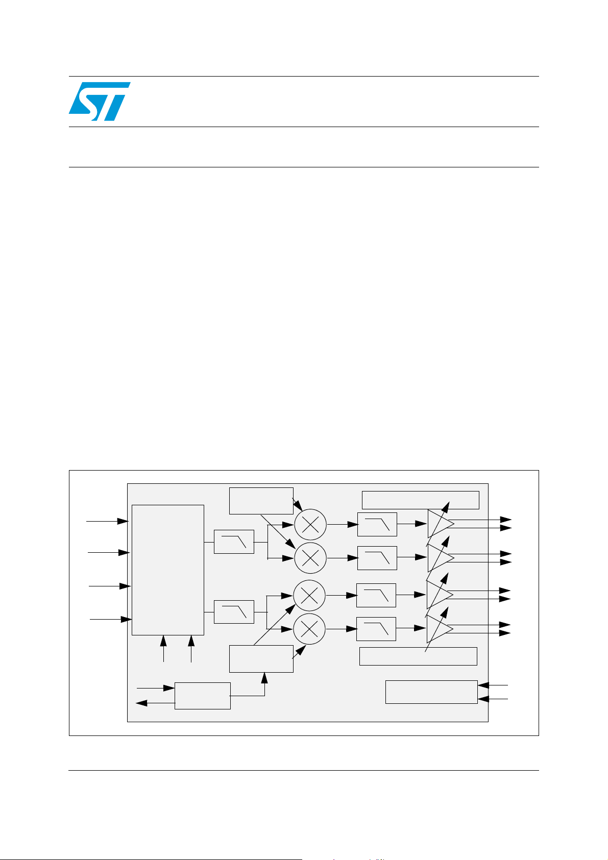
1 Introduction
The STV6120 dual tuner has four identical wideband RF inputs. The switch matrix 4:2
allows the selection of the appropriate RF input for each down-conversion path. After the
matrix, there is a high-frequency low-pass filter followed by two down mixers. Each mixer,
which down-converts the signal to baseband, is followed by a low-pass filter and amplifying
stages. The baseband gain can be varied by programming a register through the I
The local oscillator signals are provided by two integrated fractional-N PLLs. Each PLL
contains an on-chip voltage controlled oscillator, which meets stringent phase noise
requirements. The PLL loop filters are partially integrated. The local oscillator frequencies
are programmable between 250 and 2150 MHz.
The comparison frequency for the phase-frequency detector is generated by dividing the
crystal oscillator reference frequency. The crystal frequency will be in the range 16 MHz
to 30 MHz depending on the application.
The design of the STV6120 has been carefully implemented to avoid the problems
associated with having two tuners integrated on a single chip.
Features Benefits
2
C bus.
Quad tuner inputs Fits universal quad and Quattro LNB requirements
or if fewer inputs are used, very high isolation
4:2 switch matrix Low-cost, high-performance BoM integration
allowing flexibility between legacy systems and
SCR (unicable) systems
Single flexible Xtal Wide choice of crystal frequencies with robust
clock buffer to drive second tuners and
demodulators allowing eBoM savings
Fine-grained power management Allows power savings and settings optimized for
actual use conditions
Wide input frequency range Allows flexible and novel frequency planning and in
some cases BoM cost optimization
Intrinsic performance Excellent compromise between linearity and noise
figure allowing the most difficult signals to be
extracted in the most congested and noisy
conditions
Fractional-N PLL Low phase noise for low packet error rate under
extreme conditions (e.g., low symbol rates), fast
locking
2/4 Doc ID 022527 Rev 1
 Loading...