

Features
■ Capable of detecting dedicated USB chargers
and host chargers (current sink and dedicated
methods)
■ Operates with V
supply voltage ranging
BAT
from 2.2 V to 4.5 V
■ Active high open drain hardware detection pin
(DETECT)
■ GPIO control interface
■ 1.6 V - 2.8 V interface voltage range (V
■ V
■ Low DP-DM input capacitance
■ ESD: HBM ± 2 kV, CDM 500 V on every pin
■ 12 bumps Flip-Chip package, 1.6 x1.2 mm,
voltage 6 V clamping circuit
BUS
IO
)
pitch 0.4 mm, max thickness 0.60 mm,
Halogen free RoHS compliant package
Applications
■ Mobile phones
■ PDAs, MP3 players
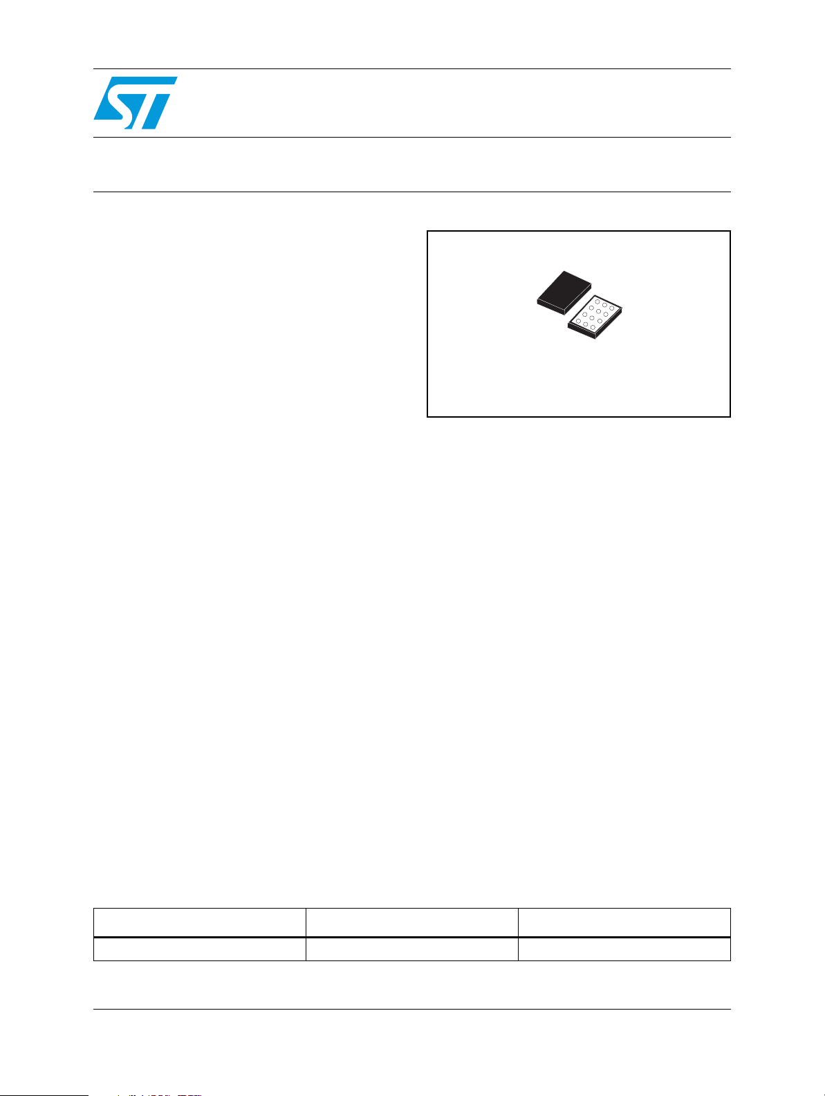
STUSBCD01B
USB charger detection interface
Flip-Chip 12 (1.6 x 1.2 mm)
Operation is controlled through three general
purpose I/O pins; a hardware open drain
detection output is also available.
An internal regulator provides the 1.8 V supply
voltage for the internal blocks and state machine
while a clamping device prevents V
from going over 6 V (typ.).
The STUSBCD01B is available in a 12 bumps
Flip-Chip 0.4 mm pitch package.
BUS
voltage
Description
The STUSBCD01B is a USB charger detection IC
which can detect dedicated USB chargers,
Host/Hub chargers or standard host ports
connected to the USB DP/DM data lines.
The device implements two different detection
methods in order to be able to distinguish
between a dedicated charger and a Host/Hub
charger.
Table 1. Device summary
Order code Package Packaging
STUSBCD01BJR Flip-Chip 12 (1.6 x 1.2 mm) 3000 parts per reel
November 2008 Rev 1 1/19
www.st.com
19

Contents STUSBCD01B
Contents
1 Application . . . . . . . . . . . . . . . . . . . . . . . . . . . . . . . . . . . . . . . . . . . . . . . . . 3
2 Pin configuration . . . . . . . . . . . . . . . . . . . . . . . . . . . . . . . . . . . . . . . . . . . 4
3 Functional description . . . . . . . . . . . . . . . . . . . . . . . . . . . . . . . . . . . . . . . 5
3.1 Detection methods . . . . . . . . . . . . . . . . . . . . . . . . . . . . . . . . . . . . . . . . . . . 5
3.2 Dedicated charger detection method . . . . . . . . . . . . . . . . . . . . . . . . . . . . . 5
3.3 Current sink method . . . . . . . . . . . . . . . . . . . . . . . . . . . . . . . . . . . . . . . . . . 5
3.4 Detection triggering . . . . . . . . . . . . . . . . . . . . . . . . . . . . . . . . . . . . . . . . . . 6
3.5 V
3.6 Internal regulator . . . . . . . . . . . . . . . . . . . . . . . . . . . . . . . . . . . . . . . . . . . . 6
clamping . . . . . . . . . . . . . . . . . . . . . . . . . . . . . . . . . . . . . . . . . . . . . . 6
BUS
4 Functional tables . . . . . . . . . . . . . . . . . . . . . . . . . . . . . . . . . . . . . . . . . . . . 8
5 Maximum ratings . . . . . . . . . . . . . . . . . . . . . . . . . . . . . . . . . . . . . . . . . . . . 9
6 Electrical characteristics . . . . . . . . . . . . . . . . . . . . . . . . . . . . . . . . . . . . 10
7 Timing diagrams . . . . . . . . . . . . . . . . . . . . . . . . . . . . . . . . . . . . . . . . . . . 12
8 Package mechanical data . . . . . . . . . . . . . . . . . . . . . . . . . . . . . . . . . . . . 14
9 Revision history . . . . . . . . . . . . . . . . . . . . . . . . . . . . . . . . . . . . . . . . . . . 18
2/19
STUSBCD01B Application
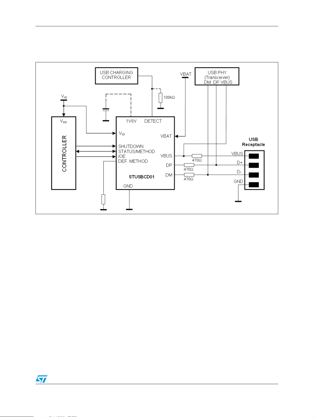
1 Application
Figure 1. Application circuit
3/19
Pin configuration STUSBCD01B
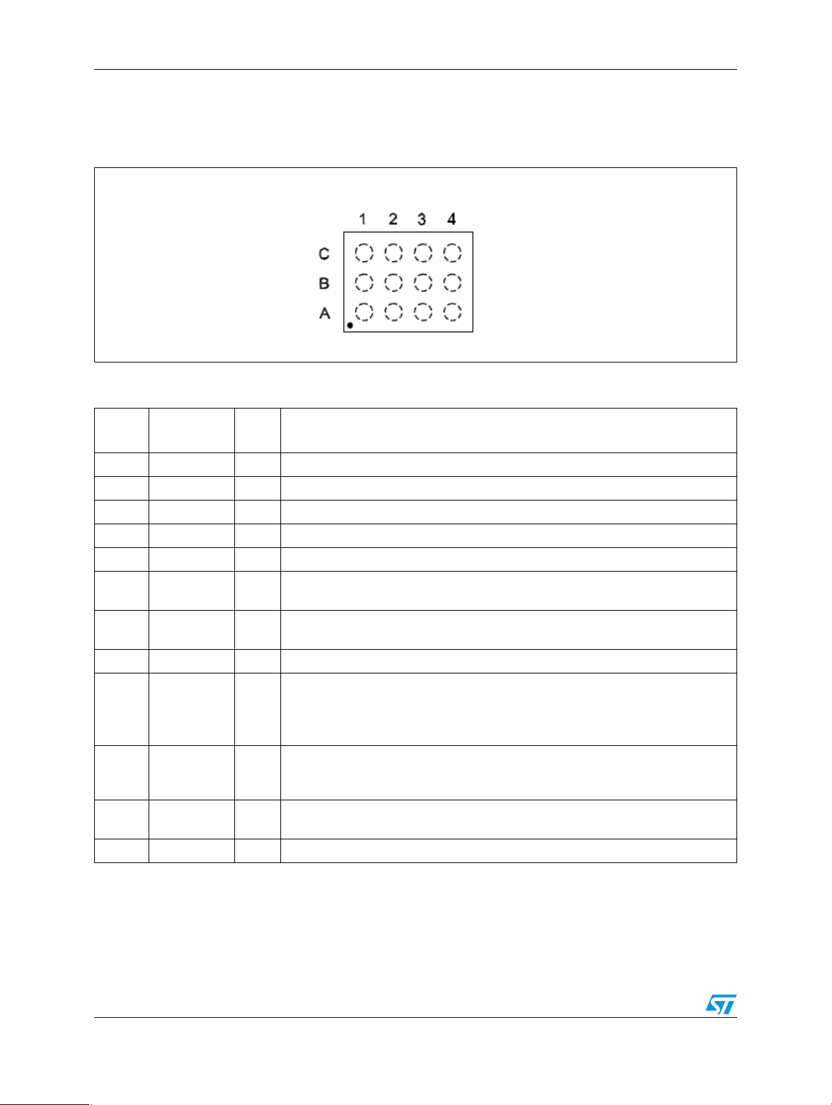
2 Pin configuration
Figure 2. Bump configuration (top through view)
Table 2. Pin description
Bump
name
Symbol Type Description
C3 VBAT PWR Analog supply voltage input (2.2 V - 4.5 V)
C2 GND PWR Ground reference
A3 V
IO
PWR Digital interface supply voltage (1.6 V - 2.8 V)
B4 DP AI/O Connected to USB D+ Data line
A4 DM AI/O Connected to USB D- Data line
B2 DETECT O
A2 SHUTDOWN I
Hardware detection pin (open drain). 300 kΩ internal pull-down resistor. V
referred.
Standby mode selection pin. Active HIGH. Terminates the detection and resets
the device.
A1 /OE I Output enable for DETECT output. Active LOW.
SW detection output: High when Charger detected. Pulled high or low through
B1
STATUS/
METHOD
internal weak pull-up to 1V8V and weak pull-down.
AI/O
Detection method selection input: low for dedicated method, high for current sink
method.
B3
DEFAULT
METHOD
C4 VBUS AI
Hardware selection for detection method. Active only if V
Dedicated method is selected if driven low, current sink method if driven high.
AI
referred. Do not leave floating to avoid increased power consumption.
V
BAT
voltage comparator input. Triggers the charger detection. 6V limited voltage
V
BUS
when 10 V are applied externally.
is not present.
IO
BAT
C1 1V8V O Regulator output voltage. Bypass capacitor not required.
4/19

STUSBCD01B Functional description
3 Functional description
The STUSBCD01B is designed to provide USB charger detection functionality to USB
platforms which do not have this feature integrated in the PHY. The device can work with a
supply voltage ranging from 2.2 V to 4.5 V and has an internal regulator which generates the
1.8 V voltage required for the internal blocks and state machine.
The STUSBCD01B can detect a dedicated charger or a Host/Hub charger connected to
USB data lines and provides both an open drain pin and a digital I/O pin for the detection
output signal. The open drain output can be disabled using the /OE input signal.
Two different detection methods, selectable through the STATUS/METHOD pin, are
implemented in order to distinguish between a dedicated charger and a Host/Hub charger. If
the interface voltage is not present the detection method is defined by the status of default
method pin.
The STUSBCD01B features very low power consumption in Standby mode and low input
capacitance on DP/DM pins. An over voltage protection circuit is also implemented on the
VBUS pin in order to limit V
connected to it.
voltage to 6 V and provide protection to external devices
BUS
3.1 Detection methods
The STUSBCD01B implements a current source/sink method to detect dedicated chargers
(wall chargers) and a current sink method for Host/Hub chargers (based on USB battery
charging spec v1.0). If a standard Host/Hub is connected to the device it is recognized
thanks to its pull-down resistors on DP/DM lines and therefore DETECT/STATUS outputs
will be low.
3.2 Dedicated charger detection method
Selected driving method pin low during the falling edge of shutdown or driving default
method pin low if V
source on DP pin and a current sink on DM pin to detect the resistor (max 200 Ω) which
connects DP and DM in dedicated chargers.
is not present. The dedicated charger detection method uses a current
IO
3.3 Current sink method
Selected driving method pin high during the falling edge of shutdown or driving default
method pin high if V
and a current of IDAT_SINK is drawn from DM.
If a Host/Hub charger is connected, STUSBCD01B will see a voltage of VDAT_SRC on pin
DM. The same happens if a dedicated charger is connected and, therefore, in order to
distinguish between the two, if the current sink method detection is successful it is
necessary to run the dedicated charger detection method immediately after.
is not present. A voltage source of VDAT_SRC is connected to DP
IO
5/19

Functional description STUSBCD01B
3.4 Detection triggering
USB Charger detection automatically starts when V
and shutdown input is low.
If V
detection is immediately terminated.
If no charger is detected (DETECT = 0 and /OE = 0), V
threshold and V
If a charger is detected, detect and status pins are kept high until V
V
Any hardware detection (V
V
3.5 V
The STUSBCD01B features a built in over voltage protection circuit which prevents V
voltage from going over 6 V. The device is able to withstand continuous voltages of up to
10 V applied to V
the voltage to 6 V within 1 µs. A 470 Ω resistor in series between V
is required. Any external device needing V
STUSBCD01B's V
Minimum input resistance for V
400 kΩ.
drops under V
BUS
TH_VBUS
threshold.
TH_IO
clamping
BUS
TH_VBUS
is not present then a new detection is started every 1 s.
IO
threshold or shutdown input is pulled high, the charger
threshold or a new detection is started.
not present) is terminated as soon as VIO voltage rises above
IO
pin through an external resistor; in this case the clamping circuit limits
BUS
over-voltage protection must be connected to
BUS
BUS
pin.
pin in normal operating conditions (up to ~ 5.3 V) is
BUS
voltage is over V
BUS
voltage is kept over V
BUS
TH_VBUS
drops under
BUS
voltage and V
BUS
threshold
BUS
BUS
pin
TH_VBUS
3.6 Internal regulator
The STUSBCD01B has an internal regulator which outputs 1.8 V (nominal) to supply
internal blocks. The regulator does not require any bypass capacitor for stability.
6/19

STUSBCD01B Functional description
Figure 3. Functional diagram
7/19

Functional tables STUSBCD01B
4 Functional tables
Table 3. Operating mode
SHUTDOWN /OE V
IO
VBAT VBUS
STATUSDETECT
Operating mode
X X X Not available X X Power down
H X Available Available Not available X
(1)
Standby (SW control)
- - Not available Available Not available L Standby (NO SW control)
L X Available Available Available L Active, SW detection
- - Not available Available Available L Active, HW detection
1. Low when value is not forced by controller.
Table 4. Output signals
V
IO
Available L Charger detected L H (pull up active) Active (driving to V
Available L Charger detected H H (pull up active) L (internally pulled down)
Available L Charger not detected X L (pull down active) L (internally pulled down)
Available H - X Input L (internally pulled down)
Not available - Charger detected - Undefined Active (driving to V
Not available - Charger not detected - Undefined L (internally pulled down)
Shutdown Detection result /OE Status/Method Detect
BAT
BAT
)
)
Table 5. Pin states during detection
Detection method DP DM
Dedicated Outputs I
Current sink Outputs V
Note: See timing diagrams for more details.
8/19
DCH_SRC
DAT_SRC
Sinks I
Sinks I
DAT_SINK
DAT_SINK

STUSBCD01B Maximum ratings
5 Maximum ratings
Table 6. Absolute maximum ratings
(1)
Symbol Parameter Value Unit
V
BAT
V
BUS
DP, DM, DETECT,
DEFAULT METHOD
V
X
T
STG
(2)
ESD
1. Exceeding the absolute maximum rating may damage the device.
2. Devices are ESD sensitive. Handling precautions recommended. Human body model, 1.5 kΩ in series with 100 pF.
Battery supply voltage 6 V
USB V
USB V
voltage 6 V
BUS
voltage with external 470 Ω resistor 12 V
BUS
Detection pins 6 V
All other pins -0.5 to 4.6 V
Storage temperature range -65 to +150 °C
Electrostatic discharge voltage (according to HBM
JESD22-A114D)
Electrostatic discharge voltage (according to CDM
JESD22-C101C)
± 2 kV
200 V
Note: Absolute maximum ratings are those values above which damage to the device may occur.
Functional operation under these conditions is not implied. All voltages are referenced to
GND.
Table 7. Recommended operating conditions
(1)
Symbol Parameter Min. Typ. Max. Unit
V
V
V
1. The device is not guaranteed to function outside its operating rating.
Analog supply voltage 2.2 4.2 4.5 V
BAT
Interface supply voltage 1.5 1.8 2.8 V
IO
V
BUS
voltage 0 5.25 V
BUS
9/19

Electrical characteristics STUSBCD01B
6 Electrical characteristics
Table 8. DC electrical characteristics (power supply and digital I/O pins)
(V
= 4.2 V, TA = 25°C, specifications over temperature, -40 to 85 °C)
BAT
(1)
Symbol Parameter Test conditions Min. Typ. Max. Unit
V
1V8V LDO regulated voltage output
I
V
TH_IOVIO
V
V
V
BAT
I
IO
supply current
BAT
VIO supply current STATUS/METHOD=”open” 5 µA
detection threshold voltage 1 V
Low level input voltage
V
IL
(Note 1)
High level input voltage
V
IH
(Note 1)
Low level input voltage
ILDM
(Note 2)
High level input voltage
IHDM
(Note 2)
Low level input leakage
I
IL
(SHUTDOWN, /OE)
High level input leakage
I
IH
(SHUTDOWN, /OE)
> V
BUS
TH_VBUS
4.5V
V
= 2.2 to 4.5V; Standby mode 20 µA
BAT
V
= 2.2 to 4.5V; Detection 1 mA
BAT
= 1.6 to 2.8V 0.15 V
V
IO
= 1.6 to 2.8V 0.85 V
V
IO
= 1.6 to 2.8V, all inputs at GND ±5 µA
V
IO
V
= 1.6 to 2.8V, all inputs at V
IO
, V
= 2.2V to
BAT
1.76 1.8 1.84 V
IO
0.85
V
BAT
IO
0.15 V
±5 µA
IO
BAT
V
V
V
V
V
V
1. Characterized specification(s), but not production tested.
Low level output voltage
OL
(STATUS)
High level output voltage
OH
(STATUS)
C
Input capacitance (Note 1)4pF
IN
= +10µA, VIO = 1.8V 0 100 mV
I
OL
= -10µA, VIO = 1.8V 1.7 1.8 V
I
OH
Note: 1 Specification applies to the following pins: /OE, SHUTDOWN, STATUS/METHOD
2 Specification applies to DEFAULT METHOD pin.
10/19

STUSBCD01B Electrical characteristics
Table 9. DC electrical characteristics (analog pins)
(V
= 4.2 V, TA = 25 °C, specifications over temperature, -40 to 85 °C)
BAT
Symbol Parameter Test conditions Min. Typ. Max. Unit
V
V
BUS
I
VBUS
V
BUS_CLMPVBUS
V
TH_VBUSVBUS
Z
IN_VBUSVBUS
C
IN
V
DAT_SRC
V
DAT_REF
I
DAT_SINK
I
DCH_SRC
V
THDPL
Z
PD_DET
V
OH_DET
1. Measured at DP pin. Includes effect of internal switches.
2. I
DAT_SRC
3. V
DAT_SINK
Table 10. AC electrical characteristics
voltage 0 5.25 V
BUS
V
current V
BUS
clamping voltage R
=0 to 5.25V 10 µA
BUS
= 470Ω 5.3 6 V
EXT
voltage detection threshold 2 4 V
input impedance V
max 5.25V 400 kΩ
BUS
DP, DM input capacitance 5 pF
Data source voltage
(1)
IDP=I
DAT_SRC
(2)
0.615 0.65 0.7 V
Data detect voltage 0.25 0.34 V
Data sink current VDM=V
Dedicated charger detection DP
source current
DAT_SINK
(3)
50 100 µA
15 30 µA
DP low threshold 0.6 V
DETECT pin pull down impedance /OE=1 240 300 360 kΩ
DETECT output driving voltage
= 0 to 200 µA according to USB specs.
= 0.15 V to 3.6 V according to USB specs.
(V
= 4.2 V, TA = 25 °C, specifications over temperature, -40 to 85 °C)
BAT
I
OH_DET
V
(1)
= 0.5mA,
= 2.2 to 4.5V
BAT
–0.2 V
V
BAT
BAT
Symbol Parameter Test conditions Min. Typ. Max. Unit
V
V
T
VBUS_DBNC
T
DP_SRC_ON
T
CHGR_DET_DBNC
T
DPSRC_HICRNT
T
D_VDAT
T
VBUS_DET_CSVBUS
T
VBUS_DET_DCVBUS
T
IDCH_SRC_ONIDCH_SRC
T
IDAT_SINK_ONIDAT_SINK
T
D_IDAT_SINKIDCH_SRC
T
PER_DET
T
W_H/L
1. All AC parameters guaranteed by design but not production tested.
2. T
IDCH_SRC_ON
= T
debounce time 5 8 ms
BUS
DP source on time Current sink method 100 170 ms
Charger detect debounce Current sink method 20 40 ms
DP source off to DETECT high
time
V
DAT_SRC
on delay Current sink method 5 8 ms
Current sink method 40 70 ms
attach to DETECT high time Current sink method 150 270 ms
attach to DETECT high time Dedicated charger method 145 248 ms
on time
(2)
Dedicated charger method 140 240 ms
on time Dedicated charger method 40 70 ms
on to I
DAT_SINK
Periodic detection period
on delay Dedicated charger method 100 170 ms
Hardware detection, No
charger
Minimum pulse width High/Low All digital inputs 2 µs
D_IDAT_SINK
+ T
IDAT_SINK_ON
11.6s
11/19

Timing diagrams STUSBCD01B
7 Timing diagrams
Figure 4. Current sink method (with charger connected)
V
V
BUS+
BUS+
V
V
BUS
BUS
V
V
DAT_SRC
DAT_SRC
Applied to DP
Applied to DP
I
I
DAT_SINK
DAT_SINK
Applied to DM
Applied to DM
T
T
VBUS_DBNC
VBUS_DBNC
5ms
5ms
V
V
BUS-
BUS-
T
T
D_VDAT
D_VDAT
5ms
5ms
T
T
DP_SRC_ON
DP_SRC_ON
>100ms
>100ms
0.615-0.7V
0.615-0.7V
50-100µA
50-100µA
T
T
VBUS_DBNC
VBUS_DBNC
5ms
5ms
DM_SRC
DM_SRC
Either returned V
Either returned V
dedicated charger or applied
dedicated charger or applied
V
V
V
V
V
V
output, see Functional
output, see Functional
Diagram) must be high
Diagram) must be high
for >20ms for charger
for >20ms for charger
detection to be valid
detection to be valid
DETECT
DETECT
DAT_SRC
DAT_SRC
DAT_DET
DAT_DET
DAT_DET
DAT_DET
by HOST charger
by HOST charger
(comparator
(comparator
DAT_SRC
DAT_SRC
T
T
T
DM_SRC_EN
if
if
150ms < T
150ms < T
DM_SRC_EN
<20ms
<20ms
T
T
VBUS_DET_CS
VBUS_DET_CS
>20ms
>20ms
CHGR_DET_DBNC
CHGR_DET_DBNC
< 270ms
< 270ms
T
DM_SRC_DIS
DM_SRC_DIS
<20ms
<20ms
>40ms
>40ms
T
T
DPSRC_HICRNT
DPSRC_HICRNT
12/19

STUSBCD01B Timing diagrams
Figure 5. Dedicated charger detection method (with charger connected)
V
V
BUS+
BUS+
V
V
BUS
BUS
I
I
DCH_SRC
DCH_SRC
Applied to DP
Applied to DP
I
I
DAT_SINK
DAT_SINK
Applied to DM
Applied to DM
T
T
VBUS_DBNC
VBUS_DBNC
V
V
BUS-
BUS-
T
T
VBUS_DBNC
VBUS_DBNC
T
T
D_IDAT_SINK
D_IDAT_SINK
T
T
IDCH_SRC_ON
IDCH_SRC_ON
T
T
IDAT_SINK_ON
IDAT_SINK_ON
15-30µA
15-30µA
50-100µA
50-100µA
DP
DP
DM
DM
DETECT
DETECT
145ms < T
145ms < T
VBUS_DET_DC
VBUS_DET_DC
< 248ms
< 248ms
13/19

Package mechanical data STUSBCD01B
8 Package mechanical data
In order to meet environmental requirements, ST offers these devices in ECOPACK®
packages. These packages have a lead-free second level interconnect. The category of
second Level Interconnect is marked on the package and on the inner box label, in
compliance with JEDEC Standard JESD97. The maximum ratings related to soldering
conditions are also marked on the inner box label. ECOPACK is an ST trademark.
ECOPACK specifications are available at: www.st.com.
14/19

STUSBCD01B Package mechanical data
Flip-Chip 12 mechanical data
mm. mils.
Dim.
Min. Typ. Max. Min. Typ. Max.
A 0.52 0.56 0.60 20.5 22.0 23.6
A1 0.17 0.20 0.23 6.7 7.99.1
A2 0.350.360.3713.8 14.2 14.6
b 0.23 0.26 0.299.1 10.2 11.4
D 1.543 1.593 1.643 60.7 62.7 64.7
D1 1.20 47.2
E 1.15 1.202 1.25 45.3 47.3 49.2
E1 0.80 31.5
e 0.40 15.7
SE 0.20 7.9
Bottom view
Bottom view
0.075
0.075
Top view
Top view
7504892-D
15/19

Package mechanical data STUSBCD01B
Tape & reel Flip-Chip 12 mechanical data
mm. inch.
Dim.
Min. Typ. Max. Min. Typ. Max.
A180 7.087
C 12.8 13.2 0.504 0.520
D 20.2 0.795
N60 2.362
T 14.4 0.567
Ao 1.43 1.48 1.53 0.056 0.058 0.060
Bo 1.71 1.76 1.81 0.067 0.069 0.071
Ko 0.75 0.800.85 0.030 0.031 0.033
Po 3.9 4.1 0.154 0.161
P 3.9 4.1 0.154 0.161
16/19

STUSBCD01B Package mechanical data
Figure 6. Footprint data (mm.)
17/19

Revision history STUSBCD01B
9 Revision history
Table 11. Document revision history
Date Revision Changes
18-Nov-2008 1 Initial release.
18/19

STUSBCD01B
Please Read Carefully:
Information in this document is provided solely in connection with ST products. STMicroelectronics NV and its subsidiaries (“ST”) reserve the
right to make changes, corrections, modifications or improvements, to this document, and the products and services described herein at any
time, without notice.
All ST products are sold pursuant to ST’s terms and conditions of sale.
Purchasers are solely responsible for the choice, selection and use of the ST products and services described herein, and ST assumes no
liability whatsoever relating to the choice, selection or use of the ST products and services described herein.
No license, express or implied, by estoppel or otherwise, to any intellectual property rights is granted under this document. If any part of this
document refers to any third party products or services it shall not be deemed a license grant by ST for the use of such third party products
or services, or any intellectual property contained therein or considered as a warranty covering the use in any manner whatsoever of such
third party products or services or any intellectual property contained therein.
UNLESS OTHERWISE SET FORTH IN ST’S TERMS AND CONDITIONS OF SALE ST DISCLAIMS ANY EXPRESS OR IMPLIED
WARRANTY WITH RESPECT TO THE USE AND/OR SALE OF ST PRODUCTS INCLUDING WITHOUT LIMITATION IMPLIED
WARRANTIES OF MERCHANTABILITY, FITNESS FOR A PARTICULAR PURPOSE (AND THEIR EQUIVALENTS UNDER THE LAWS
OF ANY JURISDICTION), OR INFRINGEMENT OF ANY PATENT, COPYRIGHT OR OTHER INTELLECTUAL PROPERTY RIGHT.
UNLESS EXPRESSLY APPROVED IN WRITING BY AN AUTHORIZED ST REPRESENTATIVE, ST PRODUCTS ARE NOT
RECOMMENDED, AUTHORIZED OR WARRANTED FOR USE IN MILITARY, AIR CRAFT, SPACE, LIFE SAVING, OR LIFE SUSTAINING
APPLICATIONS, NOR IN PRODUCTS OR SYSTEMS WHERE FAILURE OR MALFUNCTION MAY RESULT IN PERSONAL INJURY,
DEATH, OR SEVERE PROPERTY OR ENVIRONMENTAL DAMAGE. ST PRODUCTS WHICH ARE NOT SPECIFIED AS "AUTOMOTIVE
GRADE" MAY ONLY BE USED IN AUTOMOTIVE APPLICATIONS AT USER’S OWN RISK.
Resale of ST products with provisions different from the statements and/or technical features set forth in this document shall immediately void
any warranty granted by ST for the ST product or service described herein and shall not create or extend in any manner whatsoever, any
liability of ST.
ST and the ST logo are trademarks or registered trademarks of ST in various countries.
Information in this document supersedes and replaces all information previously supplied.
The ST logo is a registered trademark of STMicroelectronics. All other names are the property of their respective owners.
© 2008 STMicroelectronics - All rights reserved
STMicroelectronics group of companies
Australia - Belgium - Brazil - Canada - China - Czech Republic - Finland - France - Germany - Hong Kong - India - Israel - Italy - Japan -
Malaysia - Malta - Morocco - Singapore - Spain - Sweden - Switzerland - United Kingdom - United States of America
www.st.com
19/19
 Loading...