

General features
■ Compliant to USB V2.0 for full-speed (12Mb/s)
and low-speed (1.5Mbps) operation
■ HBM = ±14kV on D+, D– lines; ±5kV on VBUS
■ ESD Compliant to IEC-61000-4.2 (level 3) on
D+, D- lines
■ Separate I/O supply with operation down to
1.6V
■ Integrated 3.3V output LDO
■ Very low power consumption to meet USB
‘suspend’ current requirements
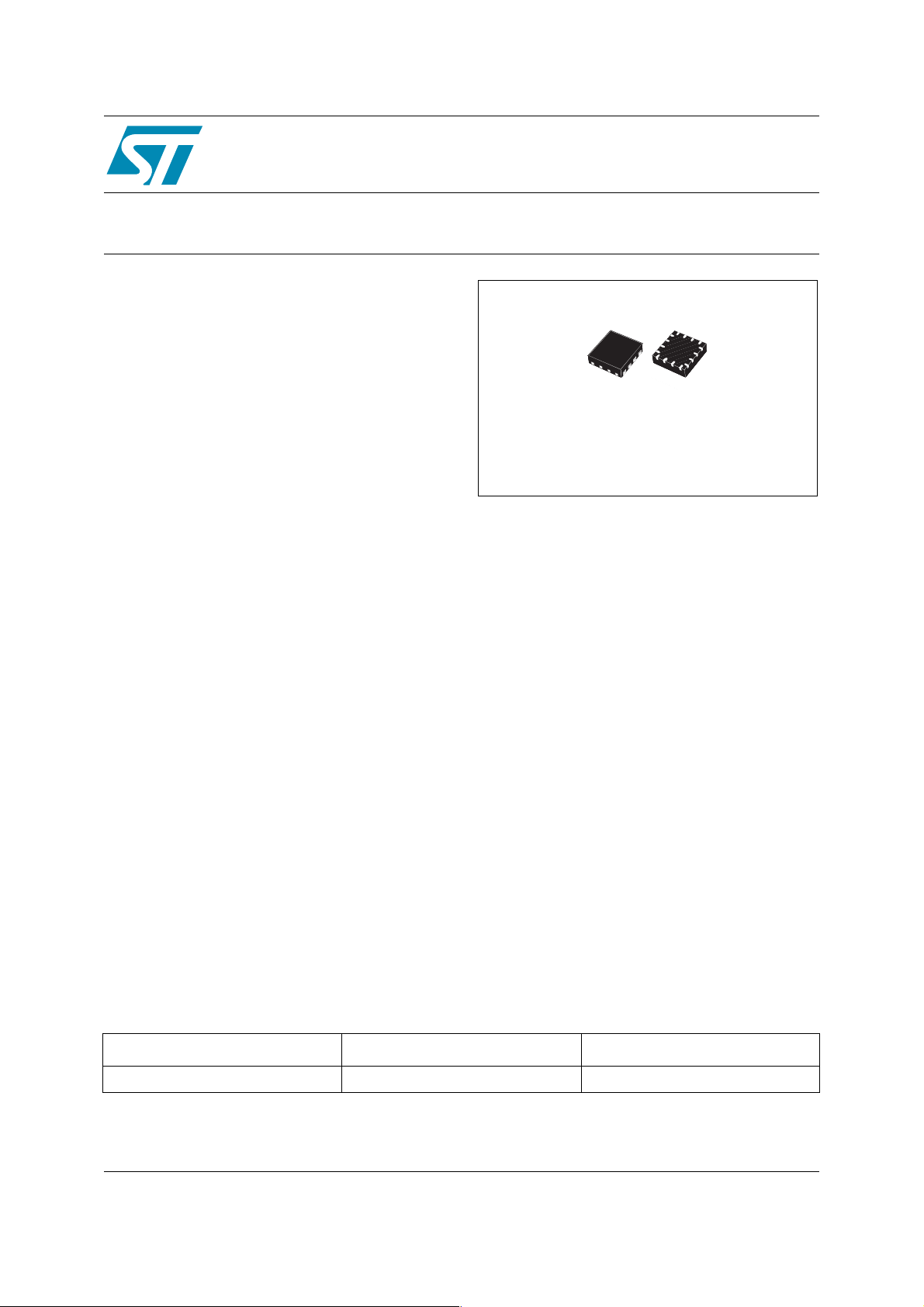
■ Small QFN16 lead free package 3x3 mm
■
No power supply sequencing requirements
■ Software controlled re-enumeration
■ Integrated D+ pull-up resistor for FS operation
2
Description
The STUSB03E is a single chip transceiver that
complies with the physical layer specifications of
the Universal Serial Bus (USB) v2.0 standard. It
has an integrated 5V to 3.3V regulator which
allows direct powering from the V
transceiver has an integrated voltage detector to
BUS
. The
STUSB03E
USB Transceiver
QFN16 (3mm x 3mm)
detect the presence of the V
features an internal D+ pull-up resistor
implemented in accordance with the 27% resistor
ECN.
The STUSB03E also supports Sharing mode
when V
is not present, which allows the D+/D–
BUS
lines to be shared with other serial protocols.
It supports both full-speed (12Mbps) and lowspeed (1.5Mbps) operation. It is also designed to
operate down to 1.6V so that it is compatible with
lower system voltages of most portable systems,
which include PDAs, MP3 Player and Cell phones.
voltage and
BUS
Order code
Part number Package Packaging
STUSB03EQR QFN16 (3mm x 3mm) 3000 parts per reel
March 2007 Rev. 2 1/20
www.st.com
20

Contents STUSB03E
Contents
1 Typical application . . . . . . . . . . . . . . . . . . . . . . . . . . . . . . . . . . . . . . . . . . . . 3
2 Pin configuration . . . . . . . . . . . . . . . . . . . . . . . . . . . . . . . . . . . . . . . . . . . . . 4
3 Functional tables . . . . . . . . . . . . . . . . . . . . . . . . . . . . . . . . . . . . . . . . . . . . . . 5
4 Maximum ratings . . . . . . . . . . . . . . . . . . . . . . . . . . . . . . . . . . . . . . . . . . . . . . 6
5 Electrical characteristics . . . . . . . . . . . . . . . . . . . . . . . . . . . . . . . . . . . . . . . 7
6 Timing diagram . . . . . . . . . . . . . . . . . . . . . . . . . . . . . . . . . . . . . . . . . . . . . . 11
7 Test circuits . . . . . . . . . . . . . . . . . . . . . . . . . . . . . . . . . . . . . . . . . . . . . . . . . 13
8 Functional description . . . . . . . . . . . . . . . . . . . . . . . . . . . . . . . . . . . . . . . . 15
9 Package mechanical data . . . . . . . . . . . . . . . . . . . . . . . . . . . . . . . . . . . . . . 16
10 Revision history . . . . . . . . . . . . . . . . . . . . . . . . . . . . . . . . . . . . . . . . . . . . . 19
2/20
STUSB03E Typical application
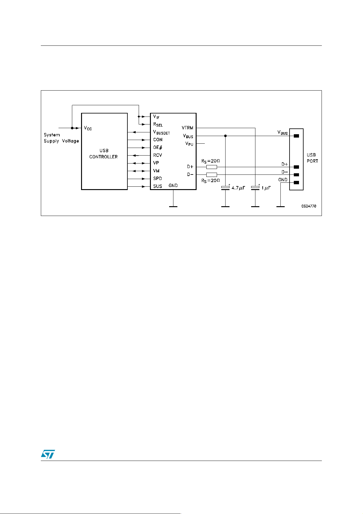
1 Typical application
Figure 1. Application circuit
3/20
Pin configuration STUSB03E
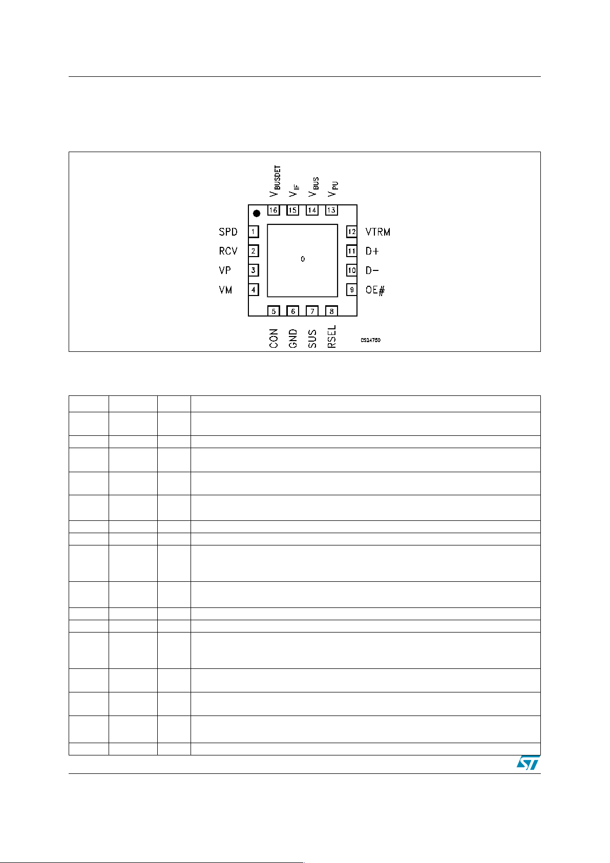
2 Pin configuration
Figure 2. Pin connections (Top View)
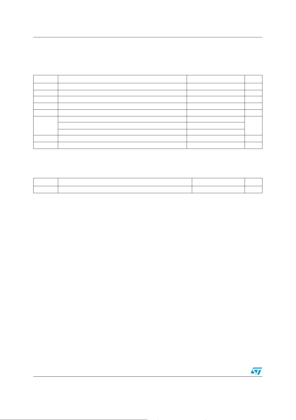
Table 1. Pin description
Pln N° Symbol I/O Name and function
1 SPD I
2 RCV O Receive Data. Output for USB differential data. (see
3 VP I/O
4 VM I/O
5CONI
6 GND Ground reference
7 SUS I Suspend (active-high). Turns off internal circuits to reduce supply current.
8 RSEL I
9OE#I
10, 11 D-, D+ I/O Differential data lines that conform to the USB v2.0 standard. (see
12 VTRM O 3.3V Reference Supply Output. Requires a 1.0µF decoupling capacitor for stability.
13
14
15
16
V
V
BUS
V
V
BUSDET
PU
IF
EXP N.C. Not connected.
Speed selection input. A logic HIGH operates at edge rates for “fullspeed” operation.
A logic LOW operates edge rates for “lowspeed” operation. See also CON pin.
Ta bl e 2
)
If OE# = H, VP = Receiver output (+)
Ta bl e 2
If OE# = L, VP = Driver input (+) (see
)
If OE# = H, VM = Receiver output (-)
Ta bl e 2
If OE# = L, VM = Driver input (-) (see
)
CONNECT (input). Connects the internal pull-up resistor to D+ if SPD and RSEL are
logic high. Controls status of VPU pin if SPD or RSEL is logic low.
Full speed pull-up resistor selection input. If RSEL = 0 the internal pull-up resistor
connected to D+ is disabled and an external resistor connected to V
pin must be
PU
used.
Output Enable (active-low). Enables transceiver data transmission onto the bus.
(see
Ta bl e 2
When not active, the transceiver is in the receive mode.
)
Ta bl e 2
Pull-up Supply Voltage Output. Used to connect 1.5K pull-up speed detect resistor
when RSEL or SPD is logic low. If CON = 0, V
O
= 3.3V ±10% (see
USB Bus Supply Voltage (4V to 5.5V). Supplies power to the USB transceiver and
I
internal circuitry.
System Interface Supply Voltage (1.6V to 3.6V). Provides reference supply voltage for
I
system I/O interface signals.
V
indicator output. When V
BUS
O
V
= Low (VIF referred).
BUSDET
Table 4.
).
> 4.0V, V
BUS
is high impedance. If CON = 1, VPU
PU
= High; when < 3.6V,
BUSDET
)
4/20
STUSB03E Functional tables
3 Functional tables
Table 2. Function selection
SUS OE# D+, D- RCV VP/VM Function
L L Driving Active Active Normal transmit mode
L H Receiving Active Active Normal receive mode
H L Hi-Z L Not Active Low power state
HHHi-ZLActive
(1) During suspend VP and VM are active in order to detect out of band signalling conditions
Receiving during suspend (low power state)
Table 3. Sharing mode pin configuration
Input/output Status
V
BUS
V
IF
D+, D-, High impedance
VP, VM High
RCV Low
SPD High impedance
V
BUSDET
V
PU
#OE, SUS, CON High impedance inputs
Floating or connected to GND
1.6V to 3.6V input
Low
High impedance
(1)
Table 4. V
Status
PU
SPD RSEL CON
H H X High impedance
H L L High impedance
HLH3.3V ± 10%
L X L High impedance
LXH3.3V ± 10%
Table 5. Truth table during normal Mode
OE# = L
Input Output
VP VM D+ D- RCV
LLLLXSE0
L H L H L Logic Low
H L H L H Logic High
HHXXXUndefined
OE# = H
Input Output
D+ D- VP VM RCV
LLLLXSE0
L H L H L Logic Low
H L H L H Logic High
HHXXXUndefined
X = Undefined
V
PU
Result
RESULT
5/20
Maximum ratings STUSB03E
4 Maximum ratings
Table 6. Absolute maximum ratings
Symbol Parameter Value Unit
V
BUS
V+ All other Inputs -0.5 to 4.6 V
I
I
ESD
T
STG
T
OPR
Absolute Maximum Ratings are those values beyond which damage to the device may occur. Functional Operation under these conditions is not implied.
Note 3. Devices are ESD sensitive. Handling precautions recommended. Human body model, 1.5k in series with 100pF.
Table 7. Thermal data
Supply Voltage 6 V
Output Current (D+, D-) ± 50 mA
O
Output Current (all others) ± 15 mA
O
I
Input Current ± 50 mA
I
D+, D-, HBM (Note 3) ± 14
V
BUS
(Note 3)
± 5
All other pins (Note 3) ± 2
Storage Temperature Range -65 to + 150 °C
Operating Temperature Range -40 to + 85 °C
kV
Symbol Parameter Value Unit
R
thJA
Thermal Resistance Junction-Ambient 59 °C/W
6/20

STUSB03E Electrical characteristics
5 Electrical characteristics
Table 8. DC electrical characteristics (system and USB interface) (VIF = 3.6V, V
otherwise noted; T
= 25°C, specifications over temperature, -40 to 85°C)
A
= 5V unless
BUS
Symbol Parameter Test conditions Min. Typ. Max. Unit
V
USB Supply Voltage 4 5.5 V
BUS
V
System I/F Supply Voltage 1.6 3.6 V
IF
V
Low Level Input Voltage (Note 4)
IL
V
High Level Input Voltage (Note 4)
IH
V
Low Level Output Voltage (Note 4)
OL
V
High Level Output Voltage (Note 4)
OH
I
Input Leakage Current (Note 4) -5 5 µA
IL
= 20µA
I
OL
= -20µA VIF-100 V
I
OH
0.85V
IF
0100mV
0.15V
IF
IF
D+, D- are idle, SUS = 1 5 µA
I
VIF Supply Current (Note 7)
IF
D+, D- active, C
SPD=1, f=6MHz, OE#=1 (Note 5)
D+, D- active, C
SPD=0, f=750kHz, OE#=1 (Note5)
D+, D- active, C
SPD=1, f=6MHz, OE#=0 (Note 5)
D+, D- active, C
SPD=0, f=750kHz, OE#=0 (Note 5)
D+, D- are idle, V
Suspend Mode (SUS = 1), OE# =
LOAD
LOAD
LOAD
LOAD
BUS
= 25pF,
= 25pF,
= 25pF,
= 25pF,
= 5.25V
2mA
220 µA
0.8 mA
120 µA
150 µA
1, SPD = 1
I
BUS
V
Supply Current
BUS
D+, D- are idle, V
SPD = 1, SUS = 0
D+, D- are idle, V
SPD = SUS = 0
D+, D- active, V
C
= 50pF, SPD = 1, f = 6 MHz
LOAD
BUS
BUS
BUS
= 5.25V
= 5.25V
= 5.25V
5mA
3.5 mA
8
OE# = SUS = 0 (Note 5)
D+, D- active, V
C
= 50pF, f = 6 MHz,
LOAD
BUS
= 5.25V
6
SUS = 0 OE# = SPD = 1 (Note 5)
D+, D- active, V
C
= 600pF, f = 750 KHz,
LOAD
BUS
= 5.25V
3.5
SUS = SPD = 0 (Note 5)
I
VPULEAKVPU
I
VIFLEAKVIF
V
PU
R
SWVPU
V
BUSDETVBUS
Note 1. Exceeding the absolute maximum rating may damage the device.
Note 2. The device is not guaranteed to function outside its operating rating.
Note 3. Devices are ESD sensitive. Handling precautions recommended. Human body model, 1.5k in series with 100pF.
Note 4. Specification applies to the following pins: SUS, SPD, RCV, CON, VP, VM, OE#, VBUSDET.
Note 5. Characterized specification(s), but not production tested.
Note 6. All AC parameters guaranteed by design but not production tested.
Note 7. RCV NOT LOADED
Leakage Current CON = 0, VPU = 0V
Leakage Current VIF = 3.6V, V
= 200µA, V
Pull-Up Output Voltage
Internal Switch Resistance I
Comparator threshold
I
TERM
= 10mA, V
TERM
Supply present 4
Supply lost 3.6
BUS
= 0V
= 4 to 5.25V
BUS
= 4 to 5.25V
BUS
-5 5 µA
-5 5 µA
33.6V
611Ω
V
V
mV
mA
V
7/20

Electrical characteristics STUSB03E
Table 9. DC electrical characteristics (system and USB interface)
(V
= 3.6V, V
IF
Symbol Parameter Test conditions Min. Typ. Max. Unit
V
V
V
V
I
I
VPULEAKVPU
I
VIFLEAKVIF
V
R
V
BUSDETVBUS
Note 1. Exceeding the absolute maximum rating may damage the device.
Note 2. The device is not guaranteed to function outside its operating rating.
Note 3. Devices are ESD sensitive. Handling precautions recommended. Human body model, 1.5k in series with 100pF.
Note 4. Specification applies to the following pins: SUS, SPD, RCV, CON, VP, VM, OE#, VBUSDET.
Note 5. Characterized specification(s), but not production tested.
Note 6. All AC parameters guaranteed by design but not production tested.
Note 7. RCV NOT LOADED
USB Supply Voltage 4 5.5 V
BUS
V
System I/F Supply Voltage 1.6 3.6 V
IF
V
Low Level Input Voltage (Note 4)
IL
High Level Input Voltage
IH
(Note 4)
Low Level Output Voltage
OL
(Note 4)
High Level Output Voltage
OH
(Note 4)
I
Input Leakage Current (Note 4) -5 5 µA
IL
I
VIF Supply Current (Note 7)
IF
BUSVBUS
Supply Current
Leakage Current CON = 1, VPU = 0V
Leakage Current VIF = 3.6V, V
Pull-Up Output Voltage
PU
SWVPU
Internal Switch Resistance I
Comparator threshold
= 5V unless otherwise noted; TA = 25°C)
BUS
IOL = 20µA
IOH = 20µA 0.9V
D+, D- are idle, SUS = 1 5 µA
D+, D- active, C
LOAD
= 25pF,
SPD=1, f=6MHz, OE#=1 (Note 5)
D+, D- active, C
LOAD
= 25pF,
SPD=0, f=750kHz, OE#=1 (Note5)
D+, D- active, C
LOAD
= 25pF,
SPD=1, f=6MHz, OE#=0 (Note 5)
D+, D- active, C
LOAD
= 25pF,
SPD=0, f=750kHz, OE#=0 (Note 5)
D+, D- are idle, V
BUS
= 5.25V
Suspend Mode (SUS = 1), OE# =
1, SPD = 1
D+, D- are idle, V
BUS
= 5.25V
SPD = 1, SUS = 0
D+, D- are idle, V
BUS
= 5.25V
SPD = SUS = 0
D+, D- active, V
C
= 50pF, SPD = 1, f = 6 MHz
LOAD
BUS
= 5.25V
OE# = SUS = 0 (Note 5)
D+, D- active, V
C
= 50pF, f = 6 MHz,
LOAD
BUS
= 5.25V
SUS = 0 OE# = SPD = 1 (Note 5)
D+, D- active, V
C
= 600pF, f = 750 KHz,
LOAD
BUS
= 5.25V
SUS = SPD = 0 (Note 5)
= 0V
BUS
I
TERM
TERM
= 200µA, V
= 10mA, V
= 4 to 5.25V
BUS
= 4 to 5.25V
BUS
Supply present 4
Supply lost 3.6
0.15V
IF
0.85V
IF
0.1 V
IF
1.3 mA
180 µA
0.4 mA
67 µA
88 100 µA
4.7 mA
3mA
5.5
5.2
3
-5 5 µA
-5 5 µA
3.3 V
9 Ω
V
V
V
mA
V
8/20

STUSB03E Electrical characteristics
Table 10. ESD performance
Symbol Parameter Test conditions Min. Typ. Max. Unit
IEC-1000-4-2 (D+, D-)
ESD
IEC-1000-4-2 (V
BUS
only)
Table 11. DC electrical characteristics (transceiver)
(V
= 3.6V, V
IF
-40 to 85°C)
Symbol Parameter Test conditions Min. Typ. Max. Unit
Hi-Z State Data Line Leakage
I
LO
(Suspend Mode)
V
Differential Input Sensitivity |(D+) - (D-)| 0.2 V
DI
V
V
Z
R
PU_D+
Differential Common Mode
CM
Range
V
Single Ended Receiver Threshold
SE
Receiver Hysteresis
RHYS
V
Static Output Low
OL
V
Static Output High
OH
C
Transceiver Capacitance Pin to GND 25 pF
I
Driver Output Resistance Steady state drive 8 24 Ω
DRV
D+ Data line pull-up resistance
= 5V unless otherwise noted; TA = 25°C, specifications over temperature,
BUS
Air Discharge (10 pulses) ± 8
Contact Discharge (10 pulses) ± 6
Air Discharge (10 pulses) ± 5
KV
Contact Discharge (10 pulses) ± 5
VI = 0 to 3.3 V, SUS = 1
Includes VDI range
-10 10 µA
0.8 2.5 V
Low to high transition 0.8 1.6 2.0 V
High to low transition 0.8 1.1 2.0 V
= 0.8 V
V
CM
= 1.5 KΩ at 3.6V (see test
R
L
circuit)
R
= 15 KΩ at GND (see test
L
circuit)
00.3V
2.8 3.6 V
100 mV
BUS idle 900 1575
Receive mode 1425 3090
Ω
Table 12. DC electrical characteristics (transceiver)
(V
= 3.6V, V
IF
Symbol Parameter Test Conditions Min. Typ. Max. Unit
Hi-Z State Data Line Leakage
I
LO
(Suspend Mode)
V
Differential Input Sensitivity |(D+) - (D-)| 0.2 V
DI
V
V
Z
R
PU_D+
(3) Pins D+, D-
Differential Common Mode
CM
Range
V
Single Ended Receiver Threshold
SE
Receiver Hysteresis
RHYS
V
Static Output Low
OL
V
Static Output High
OH
C
Transceiver Capacitance
I
Driver Output Resistance Steady state drive 16 Ω
DRV
D+ Data line pull-up resistance
= 5V unless otherwise noted; TA = 25°C)
BUS
VI = 0 to 3.3 V, SUS = 1
Includes VDI range
Low to high transition 0.8 1.6 2.0 V
High to low transition 0.8 1.1 2.0 V
= 0.8 V
V
CM
R
= 1.5 KΩ at 3.6V
L
(see
(3)
Test circuits
= 15 KΩ at GND
R
L
(see
Test circuits
Pin to GND 25 pF
)
)
BUS idle 1300
Receive mode 2200
-2 2 µA
0.8 2.5 V
50 mV
0.3 V
2.8 3.6 V
Ω
9/20

Electrical characteristics STUSB03E
Table 13. AC electrical characteristics
(V
= 3.6V, V
IF
Symbol Parameter Test Conditions Min. Typ. Max. Unit
T
Transition Rise Time (LOW SPEED)
R
T
Transition Fall Time (LOW SPEED)
F
T
V
T
V
t
TA _ OI
t
TA _ IO
t
t
t
t
PLH tPHL
t
PLH tPHL
t
PLH tPHL
Note 1. Exceeding the absolute maximum rating may damage the device.
Note 2. The device is not guaranteed to function outside its operating rating.
Note 3. Devices are ESD sensitive. Handling precautions recommended. Human body model, 1.5k in series with 100pF.
Note 4. Specification applies to the following pins: SUS, SPD, RCV, CON, RCV, VP, VM, OE#.
Note 5. Characterized specification(s), but not production tested.
Note 6. All AC parameters guaranteed by design but not production tested.
Rise/Fall Time Matching (LOW
RFM
SPEED)
Output Signal Crossover Voltage
CRS
(LOW SPEED)
T
Transition Rise Time (FULL SPEED)
R
T
Transition Fall Time (FULL SPEED)
F
Rise/Fall Time Matching (FULL
RFM
SPEED)
Output Signal Crossover Voltage
CRS
(FULL SPEED)
Output to input turnaround time
Output to input turnaround time
PZH,
Driver enable delay FS,
t
PZL
PLZ,
Driver disable delay FS,
PHZ
VP, VM to D+, D- Propagation Delay
D+, D- to RCV Propagation Delay FS, input slope = 15 ns 18 ns
D+, D- to VP, VM Propagation Delay FS, input slope = 15 ns 24 ns
= 5V unless otherwise noted; TA = 25°C.) (Note 6)
BUS
= 50pF (
C
L
Figure 5
)
CL = 600pF
= 50pF (
C
L
Figure 5
)
CL = 600pF
(TR, TF)
= 50pF (
C
L
= 50pF (
C
L
Figure 5
Figure 5
)
)
(TR, TF)
Figure 4.
Figure 4.
Figure 3.
Figure 3.
= 50pF
FS, C
L
LS, CL =600pF
75
300
75
300
ns
ns
80 125 %
1.3 2 V
420ns
420ns
90 111.11 %
1.3 2 V
05ns
05ns
50 ns
50 ns
55 ns
300 ns
10/20

STUSB03E Timing diagram
6 Timing diagram
Figure 3. Driver enable and disable delay
Figure 4. Turnaround time
Figure 5. Rise and fall times
11/20

Timing diagram STUSB03E
Figure 6. Receiver propagation delay
Figure 7. Driver propagation delay (C
Minimum Timing LS and maximum timing FS
Figure 8. FS eye diagram
= 50pF)
L
12/20

STUSB03E Test circuits
7 Test circuits
Figure 9. Load for VP, VM, RCV
Figure 10. Load for D+, D-
Figure 11. Enable and disable time circuit
Switch = GND for t
PZH
and t
; V = VTRM for t
PHZ
PZL
and t
PLZ
13/20

Test circuits STUSB03E
Figure 12. Functional diagram
14/20

STUSB03E Functional description
8 Functional description
The STUSB03E is designed to provide USB connectivity in mobile systems where available system
supply voltages are not able to satisfy USB requirements. The STUSB03E can operate down to supply
voltages of 1.6V and still meet USB physical layer specifications. As shown in the circuit above, the
STUSB03E takes advantage of the USB supply voltage, V
voltage, V
, is used to set the reference voltage used by the digital I/O lines interfacing to the system
IF
controller. Internal circuitry provides translation between the USB and system voltage domains. V
typically be the main supply voltage rail for the controller.
, to operate the transceiver. The system
BUS
IF
will
In addition, a 3.3V, 10% termination supply voltage, V
, is provided to support speed selection. VPU can
PU
be disabled or enabled under software control via the CON input. This allows for software-controlled
connect or disconnect states. A 1.5K resistor is required to be connected between this pin and the D- line
when operating in low speed mode. In full speed mode either an internal pull-up resistor or an external
one connected between V
R
pin to VIF or GND.
SEL
pin and D+ line can be used; the desired configuration is chosen by tying
PU
The use of ESD transient protection devices is not required for operation, but is recommended.
15/20

Package mechanical data STUSB03E
9 Package mechanical data
In order to meet environmental requirements, ST offers these devices in ECOPACK® packages.
These packages have a Lead-free second level interconnect. The category of second Level
Interconnect is marked on the package and on the inner box label, in compliance with JEDEC
Standard JESD97. The maximum ratings related to soldering conditions are also marked on
the inner box label. ECOPACK is an ST trademark. ECOPACK specifications are available at:
www.st.com.
16/20

STUSB03E Package mechanical data
QFN16 (3mmx3mm) MECHANICAL DATA
mm. inch
DIM.
MIN. TYP MAX. MIN. TYP. MAX.
A 0.80 0.90 1.00 0.032 0.035 0.039
A1 0.02 0.05 0.001 0.002
A3 0.20 0.008
b 0.18 0.25 0.30 0.007 0.010 0.012
D 3.00 0.118
D2 1.55 1.70 1.80 0.061 0.067 0.071
E 3.00 0.118
E2 1.55 1.70 1.80 0.061 0.067 0.071
e 0.50 0.020
K 0.20 0.008
L 0.30 0.40 0.50 0.012 0.016 0.020
r 0.09 0.006
E
A
E2
K
A1
e
D
b
D2
K
A3
L
r
This drawing is not to scale
17/20

Package mechanical data STUSB03E
Tape & Reel QFNxx/DFNxx (3x3) MECHANICAL DATA
mm. inch
DIM.
MIN. TYP MAX. MIN. TYP. MAX.
A33012.992
C 12.8 13.2 0.504 0.519
D 20.2 0.795
N 60 2.362
T 18.4 0.724
Ao 3.3 0.130
Bo 3.3 0.130
Ko 1.1 0.043
Po 4 0.157
P 8 0.315
18/20

STUSB03E Revision history
10 Revision history
Table 14. Revision history
Date Revision Changes
31-Oct-2006 1 First Release.
14-Mar-2007 2 Update tape & reel.
19/20

STUSB03E
Please Read Carefully:
Information in this document is provided solely in connection with ST products. STMicroelectronics NV and its subsidiaries (“ST”) reserve the
right to make changes, corrections, modifications or improvements, to this document, and the products and services described herein at any
time, without notice.
All ST products are sold pursuant to ST’s terms and conditions of sale.
Purchasers are solely responsible for the choice, selection and use of the ST products and services described herein, and ST assumes no
liability whatsoever relating to the choice, selection or use of the ST products and services described herein.
No license, express or implied, by estoppel or otherwise, to any intellectual property rights is granted under this document. If any part of this
document refers to any third party products or services it shall not be deemed a license grant by ST for the use of such third party products
or services, or any intellectual property contained therein or considered as a warranty covering the use in any manner whatsoever of such
third party products or services or any intellectual property contained therein.
UNLESS OTHERWISE SET FORTH IN ST’S TERMS AND CONDITIONS OF SALE ST DISCLAIMS ANY EXPRESS OR IMPLIED
WARRANTY WITH RESPECT TO THE USE AND/OR SALE OF ST PRODUCTS INCLUDING WITHOUT LIMITATION IMPLIED
WARRANTIES OF MERCHANTABILITY, FITNESS FOR A PARTICULAR PURPOSE (AND THEIR EQUIVALENTS UNDER THE LAWS
OF ANY JURISDICTION), OR INFRINGEMENT OF ANY PATENT, COPYRIGHT OR OTHER INTELLECTUAL PROPERTY RIGHT.
UNLESS EXPRESSLY APPROVED IN WRITING BY AN AUTHORIZED ST REPRESENTATIVE, ST PRODUCTS ARE NOT
RECOMMENDED, AUTHORIZED OR WARRANTED FOR USE IN MILITARY, AIR CRAFT, SPACE, LIFE SAVING, OR LIFE SUSTAINING
APPLICATIONS, NOR IN PRODUCTS OR SYSTEMS WHERE FAILURE OR MALFUNCTION MAY RESULT IN PERSONAL INJURY,
DEATH, OR SEVERE PROPERTY OR ENVIRONMENTAL DAMAGE. ST PRODUCTS WHICH ARE NOT SPECIFIED AS "AUTOMOTIVE
GRADE" MAY ONLY BE USED IN AUTOMOTIVE APPLICATIONS AT USER’S OWN RISK.
Resale of ST products with provisions different from the statements and/or technical features set forth in this document shall immediately void
any warranty granted by ST for the ST product or service described herein and shall not create or extend in any manner whatsoever, any
liability of ST.
ST and the ST logo are trademarks or registered trademarks of ST in various countries.
Information in this document supersedes and replaces all information previously supplied.
The ST logo is a registered trademark of STMicroelectronics. All other names are the property of their respective owners.
© 2007 STMicroelectronics - All rights reserved
STMicroelectronics group of companies
Australia - Belgium - Brazil - Canada - China - Czech Republic - Finland - France - Germany - Hong Kong - India - Israel - Italy - Japan -
Malaysia - Malta - Morocco - Singapore - Spain - Sweden - Switzerland - United Kingdom - United States of America
www.st.com
20/20
 Loading...