

ST STTS75 User Manual
Digital temperature sensor and thermal watchdog
Features
■ Measures temperatures from
–55 °C to +125 °C (–67 °F to +257 °F)
–
±0.5 °C (typ) accuracy
–
±2 °C (max) accuracy from
–25
°C to +100 °C
■ Low operating current: 75 µA (typ)
■ No external components required
■ 2-wire I
– Selectable serial bus address allows
■ Thermometer resolution is user-configurable
from 9 (default) to 12 bits (0.5 °C to 0.0625 °C)
■ 9-bit conversion time is 45 ms (typ)
■ Programmable temperature threshold and
hysteresis set points
■ Wide power supply range-operating voltage
range: 2.7 V to 5.5 V
■ Power saving one-shot temperature
measurement
■ Power-up defaults permit standalone operation
as thermostat
■ Shutdown mode to minimize power
consumption
■ Separate open drain output pin operates as an
interrupt or comparator/thermostat output (dual
purpose event pin)
■ Packages:
–SO8
– MSOP8 (TSSOP8)
2
C/SMBus-compatible serial interface
connection of up to eight devices on the
same bus
STTS75
SO8
MSOP8 (TSSOP8)
June 2010 Doc ID 13298 Rev 11 1/41
www.st.com
1

Contents STTS75
Contents
1 Description . . . . . . . . . . . . . . . . . . . . . . . . . . . . . . . . . . . . . . . . . . . . . . . . . 6
1.1 Serial communications . . . . . . . . . . . . . . . . . . . . . . . . . . . . . . . . . . . . . . . . 6
1.2 Temperature sensor output . . . . . . . . . . . . . . . . . . . . . . . . . . . . . . . . . . . . 6
1.3 Pin descriptions . . . . . . . . . . . . . . . . . . . . . . . . . . . . . . . . . . . . . . . . . . . . . 9
1.3.1 SDA (open drain) . . . . . . . . . . . . . . . . . . . . . . . . . . . . . . . . . . . . . . . . . . . 9
1.3.2 SCL . . . . . . . . . . . . . . . . . . . . . . . . . . . . . . . . . . . . . . . . . . . . . . . . . . . . . 9
1.3.3 OS
1.3.4 GND . . . . . . . . . . . . . . . . . . . . . . . . . . . . . . . . . . . . . . . . . . . . . . . . . . . . . 9
1.3.5 A2, A1, A0 . . . . . . . . . . . . . . . . . . . . . . . . . . . . . . . . . . . . . . . . . . . . . . . . 9
1.3.6 V
2 Operation . . . . . . . . . . . . . . . . . . . . . . . . . . . . . . . . . . . . . . . . . . . . . . . . . 10
2.1 Applications information . . . . . . . . . . . . . . . . . . . . . . . . . . . . . . . . . . . . . . 11
/INT (open drain) . . . . . . . . . . . . . . . . . . . . . . . . . . . . . . . . . . . . . . . . 9
DD . . . . . . . . . . . . . . . . . . . . . . . . . . . . . . . . . . . . . . . . . . . . . . . . . . . . . . . . . . . . . . . . . . . 9
2.2 Thermal alarm function . . . . . . . . . . . . . . . . . . . . . . . . . . . . . . . . . . . . . . 12
2.3 Comparator mode . . . . . . . . . . . . . . . . . . . . . . . . . . . . . . . . . . . . . . . . . . 12
2.4 Interrupt mode . . . . . . . . . . . . . . . . . . . . . . . . . . . . . . . . . . . . . . . . . . . . . 13
2.5 Fault tolerance . . . . . . . . . . . . . . . . . . . . . . . . . . . . . . . . . . . . . . . . . . . . . 14
2.6 Shutdown mode . . . . . . . . . . . . . . . . . . . . . . . . . . . . . . . . . . . . . . . . . . . . 14
2.7 Temperature data format . . . . . . . . . . . . . . . . . . . . . . . . . . . . . . . . . . . . . 15
2.8 Bus timeout feature . . . . . . . . . . . . . . . . . . . . . . . . . . . . . . . . . . . . . . . . . 15
2.9 One-shot mode . . . . . . . . . . . . . . . . . . . . . . . . . . . . . . . . . . . . . . . . . . . . . 16
3 Functional description . . . . . . . . . . . . . . . . . . . . . . . . . . . . . . . . . . . . . . 17
3.1 Registers and register set formats . . . . . . . . . . . . . . . . . . . . . . . . . . . . . . 17
3.1.1 Command/pointer register . . . . . . . . . . . . . . . . . . . . . . . . . . . . . . . . . . . 17
3.1.2 Configuration register . . . . . . . . . . . . . . . . . . . . . . . . . . . . . . . . . . . . . . 18
3.1.3 Temperature register . . . . . . . . . . . . . . . . . . . . . . . . . . . . . . . . . . . . . . . 19
3.1.4 Overlimit temperature register (T
3.1.5 Hysteresis temperature register (T
3.2 Power-up default conditions . . . . . . . . . . . . . . . . . . . . . . . . . . . . . . . . . . . 20
) . . . . . . . . . . . . . . . . . . . . . . . . . . . 19
OS
) . . . . . . . . . . . . . . . . . . . . . . . . . 20
HYS
3.3 Serial interface . . . . . . . . . . . . . . . . . . . . . . . . . . . . . . . . . . . . . . . . . . . . . 21
3.4 2-wire bus characteristics . . . . . . . . . . . . . . . . . . . . . . . . . . . . . . . . . . . . . 21
3.4.1 Bus not busy . . . . . . . . . . . . . . . . . . . . . . . . . . . . . . . . . . . . . . . . . . . . . 21
2/41 Doc ID 13298 Rev 11

STTS75 Contents
3.4.2 Start data transfer . . . . . . . . . . . . . . . . . . . . . . . . . . . . . . . . . . . . . . . . . 21
3.4.3 Stop data transfer . . . . . . . . . . . . . . . . . . . . . . . . . . . . . . . . . . . . . . . . . 21
3.4.4 Data valid . . . . . . . . . . . . . . . . . . . . . . . . . . . . . . . . . . . . . . . . . . . . . . . . 22
3.4.5 Acknowledge . . . . . . . . . . . . . . . . . . . . . . . . . . . . . . . . . . . . . . . . . . . . . 23
3.5 READ mode . . . . . . . . . . . . . . . . . . . . . . . . . . . . . . . . . . . . . . . . . . . . . . . 24
3.6 WRITE mode . . . . . . . . . . . . . . . . . . . . . . . . . . . . . . . . . . . . . . . . . . . . . . 26
4 Typical operating characteristics . . . . . . . . . . . . . . . . . . . . . . . . . . . . . 28
5 Maximum ratings . . . . . . . . . . . . . . . . . . . . . . . . . . . . . . . . . . . . . . . . . . . 29
6 DC and AC parameters . . . . . . . . . . . . . . . . . . . . . . . . . . . . . . . . . . . . . . 30
7 Package mechanical data . . . . . . . . . . . . . . . . . . . . . . . . . . . . . . . . . . . . 33
8 Part numbering . . . . . . . . . . . . . . . . . . . . . . . . . . . . . . . . . . . . . . . . . . . . 38
9 Package marking information . . . . . . . . . . . . . . . . . . . . . . . . . . . . . . . . 39
10 Revision history . . . . . . . . . . . . . . . . . . . . . . . . . . . . . . . . . . . . . . . . . . . 40
Doc ID 13298 Rev 11 3/41

List of tables STTS75
List of tables
Table 1. Signal names . . . . . . . . . . . . . . . . . . . . . . . . . . . . . . . . . . . . . . . . . . . . . . . . . . . . . . . . . . . . 7
Table 2. Fault tolerance setting . . . . . . . . . . . . . . . . . . . . . . . . . . . . . . . . . . . . . . . . . . . . . . . . . . . . 14
Table 3. Shutdown mode and one-shot mode description . . . . . . . . . . . . . . . . . . . . . . . . . . . . . . . . 14
Table 4. Relationship between temperature and digital output. . . . . . . . . . . . . . . . . . . . . . . . . . . . . 15
Table 5. Command/pointer register format . . . . . . . . . . . . . . . . . . . . . . . . . . . . . . . . . . . . . . . . . . . . 17
Table 6. Register pointers selection summary . . . . . . . . . . . . . . . . . . . . . . . . . . . . . . . . . . . . . . . . . 17
Table 7. Configuration register format . . . . . . . . . . . . . . . . . . . . . . . . . . . . . . . . . . . . . . . . . . . . . . . 18
Table 8. Programmable resolution configurations . . . . . . . . . . . . . . . . . . . . . . . . . . . . . . . . . . . . . . 18
Table 9. Temperature register format . . . . . . . . . . . . . . . . . . . . . . . . . . . . . . . . . . . . . . . . . . . . . . . . 19
Table 10. T
Table 11. STTS75 serial bus slave addresses . . . . . . . . . . . . . . . . . . . . . . . . . . . . . . . . . . . . . . . . . . 21
Table 12. Absolute maximum ratings . . . . . . . . . . . . . . . . . . . . . . . . . . . . . . . . . . . . . . . . . . . . . . . . . 29
Table 13. Operating and AC measurement conditions . . . . . . . . . . . . . . . . . . . . . . . . . . . . . . . . . . . . 30
Table 14. DC and AC characteristics . . . . . . . . . . . . . . . . . . . . . . . . . . . . . . . . . . . . . . . . . . . . . . . . . 31
Table 15. AC characteristics . . . . . . . . . . . . . . . . . . . . . . . . . . . . . . . . . . . . . . . . . . . . . . . . . . . . . . . . 32
Table 16. SO8 – 8-lead plastic small outline (4.90 mm x 3.90 mm) package mechanical data . . . . . 34
Table 17. MSOP8 (TSSOP8) – 8-lead, thin shrink small outline (3 mm x 3 mm) package
Table 18. Carrier tape dimensions for SO8 and MSOP8 (TSSOP8) packages . . . . . . . . . . . . . . . . . 36
Table 19. Reel dimensions for 12 mm carrier tape - SO8 and MSOP8 (TSSOP8) packages . . . . . . 37
Table 20. Ordering information scheme . . . . . . . . . . . . . . . . . . . . . . . . . . . . . . . . . . . . . . . . . . . . . . . 38
Table 21. Document revision history . . . . . . . . . . . . . . . . . . . . . . . . . . . . . . . . . . . . . . . . . . . . . . . . . 40
and T
OS
mechanical data . . . . . . . . . . . . . . . . . . . . . . . . . . . . . . . . . . . . . . . . . . . . . . . . . . . . . . . . . 35
register format . . . . . . . . . . . . . . . . . . . . . . . . . . . . . . . . . . . . . . . . . . . . . . . 20
HYS
4/41 Doc ID 13298 Rev 11

STTS75 List of figures
List of figures
Figure 1. Logic diagram . . . . . . . . . . . . . . . . . . . . . . . . . . . . . . . . . . . . . . . . . . . . . . . . . . . . . . . . . . . . 7
Figure 2. Connections (SO8, TSSOP8) . . . . . . . . . . . . . . . . . . . . . . . . . . . . . . . . . . . . . . . . . . . . . . . . 8
Figure 3. Functional block diagram . . . . . . . . . . . . . . . . . . . . . . . . . . . . . . . . . . . . . . . . . . . . . . . . . . . 8
Figure 4. Typical 2-wire interface connection diagram . . . . . . . . . . . . . . . . . . . . . . . . . . . . . . . . . . . 11
Figure 5. OS
Figure 6. Serial bus data transfer sequence . . . . . . . . . . . . . . . . . . . . . . . . . . . . . . . . . . . . . . . . . . . 22
Figure 7. Acknowledgement sequence . . . . . . . . . . . . . . . . . . . . . . . . . . . . . . . . . . . . . . . . . . . . . . . 23
Figure 8. Slave address location . . . . . . . . . . . . . . . . . . . . . . . . . . . . . . . . . . . . . . . . . . . . . . . . . . . . 24
Figure 9. Typical 2-byte READ from preset pointer location (e.g. temp - T
Figure 10. Typical pointer set followed by an immediate READ for 2-byte register (e.g. temp). . . . . . 25
Figure 11. Typical 1-byte READ from the configuration register with preset pointer . . . . . . . . . . . . . . 25
Figure 12. Typical pointer set followed by an immediate READ from the configuration register . . . . . 26
Figure 13. Configuration register WRITE . . . . . . . . . . . . . . . . . . . . . . . . . . . . . . . . . . . . . . . . . . . . . . . 26
Figure 14. T
Figure 15. Temperature variation vs. voltage . . . . . . . . . . . . . . . . . . . . . . . . . . . . . . . . . . . . . . . . . . . 28
Figure 16. Bus timing requirements sequence . . . . . . . . . . . . . . . . . . . . . . . . . . . . . . . . . . . . . . . . . . 32
Figure 17. SO8 – 8-lead plastic small outline (4.90 mm x 3.90 mm) package mechanical drawing . . 34
Figure 18. MSOP8 (TSSOP8) – 8-lead, thin shrink small outline (3 mm x 3 mm) package
Figure 19. Carrier tape for SO8 and MSOP8 (TSSOP8) packages . . . . . . . . . . . . . . . . . . . . . . . . . . . 36
Figure 20. Reel schematic . . . . . . . . . . . . . . . . . . . . . . . . . . . . . . . . . . . . . . . . . . . . . . . . . . . . . . . . . . 37
Figure 21. Device topside marking information (SO8) . . . . . . . . . . . . . . . . . . . . . . . . . . . . . . . . . . . . . 39
Figure 22. Device topside marking information (MSOP8/TSSOP8). . . . . . . . . . . . . . . . . . . . . . . . . . . 39
output temperature response diagram . . . . . . . . . . . . . . . . . . . . . . . . . . . . . . . . . . . . . 13
, T
) . . . . . . . . . . . . 25
HYS
OS
and T
OS
WRITE. . . . . . . . . . . . . . . . . . . . . . . . . . . . . . . . . . . . . . . . . . . . . . . . . . . . . 27
HYS
mechanical drawing . . . . . . . . . . . . . . . . . . . . . . . . . . . . . . . . . . . . . . . . . . . . . . . . . . . . . . 35
Doc ID 13298 Rev 11 5/41

Description STTS75
1 Description
The STTS75 is a high-precision CMOS (digital) temperature sensor IC with a delta-sigma
analog-to-digital (ADC) converter and an I
for general applications such as personal computers, system thermal management,
electronics equipment, and industrial controllers, and is packaged in the industry standard
8-lead MSOP(TSSOP) and SO8 packages.
The device contains a band gap temperature sensor and programmable 9- to 12-bit ADC
which monitor and digitize the temperature to a resolution up to 0.0625 °C. The STTS75 is
typically accurate to (±3 °C - max) over the full temperature measurement range of
–55 °C to 125 °C with ±2 °C accuracy in the –25 °C to +100 °C range. At power-up, the
STTS75 defaults to 9-bit resolution for software compatibility with the STLM75.
The STTS75 is specified for operating at supply voltages from 2.7 V to 5.5 V. Operating at
3.3 V, the supply current is typically (75 µA).
The onboard delta-sigma analog-to-digital converter (ADC) converts the measured
temperature to a digital value that is calibrated in °C; for Fahrenheit applications a lookup
table or conversion routine is required.
The STTS75 is factory-calibrated and requires no external components to measure
temperature.
1.1 Serial communications
The STTS75 has a simple 2-wire I2C-compatible digital serial interface which allows the
user to access the data in the temperature register at any time. It communicates via the
serial interface with a master controller which operates at speeds up to 400 kHz. Three pins
(A0, A1, and A2) are available for address selection, and enable the user to connect up to 8
devices on the same bus without address conflict.
2
C-compatible serial digital interface. It is targeted
In addition, the serial interface gives the user easy access to all STTS75 registers to
customize operation of the device.
1.2 Temperature sensor output
The STTS75 temperature sensor has a dedicated open drain overlimit signal/alert
(OS
/INT/Alert) output which features a thermal alarm function. This function provides a
user-programmable trip and turn-off temperature. It can operate in either of two selectable
modes:
● Section 2.3: Comparator mode, and
● Section 2.4: Interrupt mode.
At power-up the STTS75 comes up in 9-bit mode and immediately begins measuring the
temperature and converting the temperature to a digital value. The resolution of the digital
output data is user-configurable to 9, 10, 11, or 12 bits which correspond to temperature
increments of 0.5 °C, 0.25 °C, 0.125 °C, and 0.0625 °C, respectively.
6/41 Doc ID 13298 Rev 11
STTS75 Description
The measured temperature value is compared with a temperature limit (which is stored in
the 16-bit (T
the 16-bit (T
OS
/INT pin is activated (see Figure 3 on page 8).
) READ/WRITE register), and the hysteresis temperature (which is stored in
OS
) READ/WRITE register). If the measured value exceeds these limits, the
HYS
Figure 1. Logic diagram
V
DD
(1)
SDA
SCL
O.S./INT
1. SDA and OS/INT are open drain.
(1)
Note: See Pin descriptions on page 9 for details.
Table 1. Signal names
Pin Symbol/name Type/direction Description
DD
(1)
(1)
2
1
0
Input/output Serial data input/output
Output Overlimit signal/interrupt alert output
Input Address2 input
Input Address1 input
Input Address0 input
Supply power Supply voltage (2.7 V to 5.5 V)
1SDA
2 SCL Input Serial clock input
3OS/INT
4 GND Supply ground Ground
5A
6A
7A
8V
1. SDA and OS/INT are open drain.
STTS75
GND
A
0
A
1
A
2
AI11840
Note: See Pin descriptions on page 9 for details.
Doc ID 13298 Rev 11 7/41
Description STTS75
Figure 2. Connections (SO8, TSSOP8)
(1)
O.S./INT
1. SDA and OS/INT are open drain.
SDA
GND
SCL
(1)
1
2
3
4
V
8
7
6
5
DD
A
0
A
1
A
2
AI11841
Note: See Pin descriptions on page 9 for details.
Figure 3. Functional block diagram
Temperature
Sensor and
Analog-to-Digital
Converter (ADC)
Σ-Δ
V
DD
A
0
A
1
A
2
Configuration Register
Temperature Register
THYS Set Point Register
TOS Set Point Register
2-wire I2C Interface
Pointer Register
Control and Logic
Comparator
GND
O.S.
SDA
SCL
AI11833a
8/41 Doc ID 13298 Rev 11

STTS75 Description
1.3 Pin descriptions
See Figure 1 on page 7 and Table 1 on page 7 for a brief overview of the signals connected
to this device.
1.3.1 SDA (open drain)
This is the serial data input/output pin for the 2-wire serial communication port.
1.3.2 SCL
This is the serial clock input pin for the 2-wire serial communication port.
1.3.3 OS/INT (open drain)
This is the overlimit signal/interrupt alert output pin. It is open drain, so it needs a pull-up
resistor.
Note: The open drain thermostat output that indicates if the temperature has exceeded user-
programmable limits (over/under temperature indicator).
1.3.4 GND
Ground; it is the reference for the power supply. It must be connected to system ground.
1.3.5 A2, A1, A0
A2, A1, and A0 are selectable address pins for the 3LSBs of the I2C interface address. They
can be set to V
1.3.6 V
DD
This is the supply voltage pin and ranges from +2.7 V to +5.5 V.
or GND to provide 8 unique address selections.
DD
Doc ID 13298 Rev 11 9/41

Operation STTS75
2 Operation
After each temperature measurement and analog-to-digital conversion, the STTS75 stores
the temperature as a 16-bit two’s complement number in the 2-byte temperature register.
The most significant bit (S, bit 15) indicates if the temperature is positive or negative:
● for positive numbers S = 0, and
● for negative numbers S = 1.
The most recently converted digital measurement can be read from the temperature register
at any time. Since temperature conversions are performed in the background, reading the
temperature register does not affect the operation in progress.
Bits 3 through 0 of the temperature register are hardwired to logic '0.' When the STTS75 is
configured for 12-bit resolution, the 12 MSBs (bits 15 through 4) of the temperature register
will contain temperature data. For 11-bit resolution, the 11 MSBs (bits 15 through 5) of the
temperature register will contain data, and bit 4 will read out as logic '0.' For 10-bit
resolution, the 10 MSBs (bits 15 through 6) will contain data, and for 9-bit resolution the
9 MSBs (bits 15 through 7) will contain data and all unused LSBs will contain '0s.'
Table 4 on page 15 gives examples of 12-bit resolution digital output data and the
corresponding temperatures. The data is compared to the values in the T
registers, and then the OS
operating mode. The number of T
/INT is updated based on the result of the comparison and the
OS
and T
bits used during the thermostat comparison
HYS
is equal to the conversion resolution set by the FT1 and FT0 bits in the configuration
register. For example, if the resolution is 9 bits, only the 9 MSBs of T
OS
used by the thermostat comparator. The alarm fault tolerance is controlled by the FTI and
FTO bits in the configuration register. They are used to set up a fault queue. This prevents
false tripping of the OS
/INT pin when the STTS75 is used in a noisy environment (see
Table 2 on page 14).
OS
and T
and T
HYS
HYS
will be
The STTS75 also supports a special one-shot mode feature that performs a single
temperature measurement and returns to shutdown mode. This is especially useful for lowpower applications. This features is accessed by first putting the device in shutdown mode,
then enabling the one-shot mode (OSM) bit in the configuration register.
The active state of the OS
/INT output can be changed via the polarity (POL) bit in the
configuration register. The power-up default is active-low.
If the user does not wish to use the thermostat capabilities of the STTS75, the OS
output should be left floating.
Note: If the thermostat is not used, the T
system data.
OS
and T
/INT
registers can be used for general storage of
HYS
10/41 Doc ID 13298 Rev 11
STTS75 Operation
2.1 Applications information
STTS75 digital temperature sensors are optimal for thermal management and thermal
protection applications. They require no external components for operations except for pullup resistors on SCL, SDA, and OS
The sensing device of STTS75 is the chip itself. The typical interface connection for this type
of digital sensor is shown in Figure 4 on page 11.
Intended applications include:
● System thermal management
● Computers/disk drivers
● Electronics/test equipment
● Power supply modules
● Consumer products
● Battery management
● Fax/printers management
● Automotive
Figure 4. Typical 2-wire interface connection diagram
/INT outputs. A 0.1 µF bypass capacitor is recommended.
Pull-up
V
DD
10kΩ
1. SDA and OS/INT are open drain.
STTS75
O.S./INT
A
0
A
1
A
2
(1)
SDA
V
DD
SCL
(1)
GND
0.1μF
V
DD
Pull-up
V
10kΩ 10kΩ
I2C Address = 1001000 (1001A2A1A0)
DD
Master
Device
AI11832
Doc ID 13298 Rev 11 11/41

Operation STTS75
2.2 Thermal alarm function
The STTS75 thermal alarm function provides user-programmable thermostat capability and
allows the STTS75 to function as a standalone thermostat without using the serial interface.
The OS
/INT output is the alarm output. This signal is an open drain output, and at power-up,
this pin is configured with active-low polarity by default.
2.3 Comparator mode
In comparator mode, each time a temperature-to-digital (T-to-D) temperature conversion
occurs, the new digital temperature is compared to the value stored in the T
registers. If a fault tolerance number of consecutive temperature measurements are greater
than the value stored in the T
register, the OS/INT output will be activated.
OS
For example, if the FT1 and FT0 bits are equal to “10” (fault tolerance = 4), four consecutive
temperature measurements must exceed T
OS
/INT output is active, it will remain active until the first time the measured temperature
drops below the temperature stored in the T
When the thermostat is in comparator mode, the OS
with any amount of hysteresis. The OS
temperature exceeds the T
value a consecutive number of times as defined by the FT1
OS
/INT output becomes active when the measured
and FT0 fault tolerance (FT) bits in the configuration register. The OS
when the temperature falls below the value stored in T
to activate the OS/INT output. Once the
OS
register.
HYS
/INT can be programmed to operate
/INT then stays active
register for a consecutive number
HYS
of times as defined by the fault tolerance bits (FT1 and FT0). Putting the device into
shutdown mode does not clear OS
/INT in comparator mode.
OS
and T
HYS
12/41 Doc ID 13298 Rev 11
STTS75 Operation
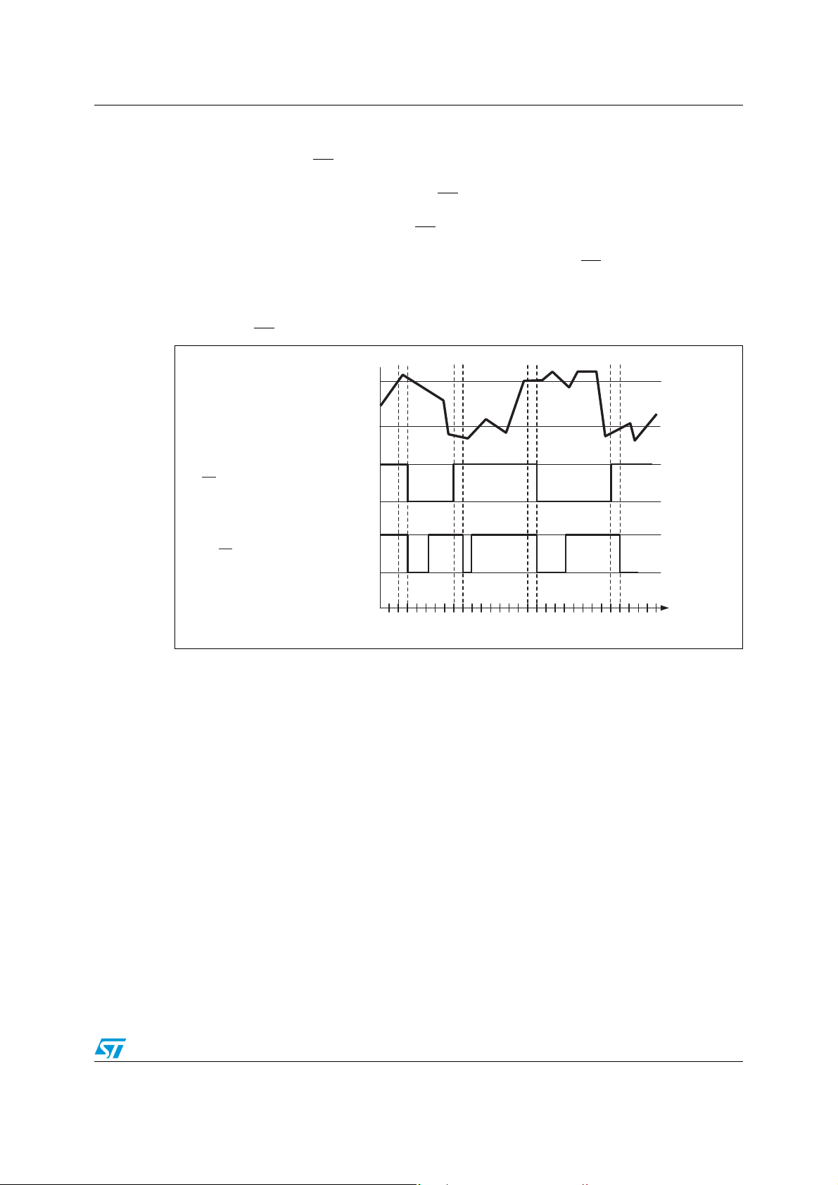
2.4 Interrupt mode
In Interrupt mode, the OS/INT output first becomes active when the measured temperature
exceeds the T
configuration register. Once activated, the OS
STTS75 into shutdown mode or by reading from any register (temperature, configuration,
T
, or T
OS
HYS
reactivated when the measured temperature falls below the T
number of times equal to the FT value. Figure 5 illustrates typical OS
response for STTS75 configured to have a fault tolerance of 2. The interrupt/clear process is
cyclical between T
value a consecutive number of times equal to the FT value in the
OS
/INT can only be cleared by either putting the
) on the device. Once the OS/INT has been deactivated, it will only be
value a consecutive
HYS
output temperature
OS
and T
HYS
.
Figure 5. OS
output temperature response diagram
T
OS
Temperature
T
HYS
Inactive
OS Output - Comparator mode
Active
Inactive
OS Output - Interrupt mode
Active
(1)(1)
(1)
Conversions
1. This assumes that a READ has occurred.
Note: The STTS75 is configured to have a fault tolerance of 2 in this example.
AI12224b
Doc ID 13298 Rev 11 13/41
 Loading...