

2.3 V memory module temperature sensor
Features
■ 2.3 V memory module temperature sensor with
integrated 2 Kb SPD EEPROM
■ Forward compatible with JEDEC TSE 2002a2
and backward compatible with STTS424E02
■ Operating temperature range:
– –40 °C to +125 °C
■ Single supply voltage: 2.3 V to 3.6 V
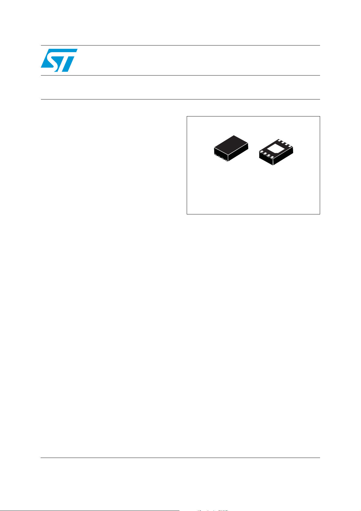
■ 2 mm x 3 mm TDFN8, height: 0.80 mm (max)
– JEDEC MO-229, WCED-3 compliant
■ RoHS compliant, halogen-free
Temperature sensor
■ Temperature sensor resolution:
programmable (9-12 bits)
0.25 °C (typ)/LSB - (10-bit) default
■ Temperature sensor accuracy (max):
– ± 1 °C from +75 °C to +95 °C
– ± 2 °C from +40 °C to +125 °C
– ± 3 °C from –40 °C to +125 °C
■ ADC conversion time: 125 ms (max) at default
resolution (10-bit)
■ Typical operating supply current: 160 µA
(EEPROM standby)
■ Temperature hysteresis selectable set points
from: 0, 1.5, 3, 6.0 °C
■ Supports SMBus timeout 25 ms - 35 ms
STTS2002
with a 2 Kb SPD EEPROM
Data brief
TDFN8
2 mm x 3 mm
(max height 0.80 mm)
2 Kb SPD EEPROM
■ Functionality identical to ST’s M34E02 SPD
EEPROM
■ Permanent and reversible software data
protection for the lower 128 bytes
■ Byte and page write (up to 16 bytes)
■ Self-time WRITE cycle (5 ms, max)
■ Automatic address incrementing
Two-wire bus
■ Two-wire SMBus/I
interface
■ Supports up to 400 kHz transfer rate
■ Does not initiate clock stretching
2
C - compatible serial
September 2010 Doc ID 17216 Rev 2 1/9
For further information contact your local STMicroelectronics sales office.
www.st.com
1

Description STTS2002
1 Description
The STTS2002 is targeted for DIMM modules in mobile personal computing platforms
(laptops), servers and other industrial applications. The thermal sensor (TS) in the
STTS2002 is compliant with the JEDEC specification TSE2002a2, which defines memory
module thermal sensors requirements for mobile platforms. The 2 Kb serial presence detect
(SPD) I
STTS2002 is organized as 256 x8 bits and is functionally identical to the industry standard
M34E02.
The TS-SPD EEPROM combination provides space as well as cost savings for mobile and
server platform dual inline memory modules (DIMM) manufacturers, as it is packaged in the
compact 2 mm x 3 mm 8-lead TDFN package with a thinner maximum height of 0.80 mm.
The DN package is compliant to JEDEC MO-229, variation WCED-3.
The digital temperature sensor has a programmable 9-12 bit analog-to-digital converter
(ADC) which monitors and digitizes the temperature to a resolution of up to 0.0625 °C. The
default resolution is 0.25 °C/LSB (10-bit). The typical accuracies over these temperature
ranges are:
2
C-compatible electrically erasable programmable memory (EEPROM) in the
±2 °C over the full temperature measurement range of –40 °C to 125 °C
±1 °C in the +40 °C to +125 °C active temperature range, and
±0.5 °C in the +75 °C to +95 °C monitor temperature range
The temperature sensor in the STTS2002 is specified for operating at supply voltages from
2.3 V to 3.6 V. Operating at 3.3 V, the typical supply current is 160 µA (includes SMBus
communication current).
The on-board sigma delta ADC converts the measured temperature to a digital value that is
calibrated in °C. For Fahrenheit applications, a lookup table or conversion routine is
required. The STTS2002 is factory-calibrated and requires no external components to
measure temperature.
The digital temperature sensor component has user-programmable registers that provide
the capabilities for DIMM temperature-sensing applications. The open drain event output pin
is active when the monitoring temperature exceeds a programmable limit, or it falls above or
below an alarm window. The user has the option to set the event output as a critical
temperature output. This pin can be configured to operate in either a comparator mode for
thermostat operation or in interrupt mode.
The 2 Kb serial EEPROM memory in the STTS2002 has the ability to permanently lock the
data in its first half (upper) 128 bytes (locations 00h to 7Fh). This feature has been designed
specifically for use in DRAM DIMMs with SPD. All of the information concerning the DRAM
module configuration (e.g. access speed, size, and organization) can be kept write
protected in the first half of the memory. The second half (lower) 128 bytes of the memory
can be write protected using two different software write protection mechanisms.
By sending the device a specific sequence, the first 128 bytes of the memory become write
protected: permanently or resettable. In the STTS2002 the write protection of the memory
array is dependent on whether the software protection has been set.
2/9 Doc ID 17216 Rev 2
STTS2002 Description
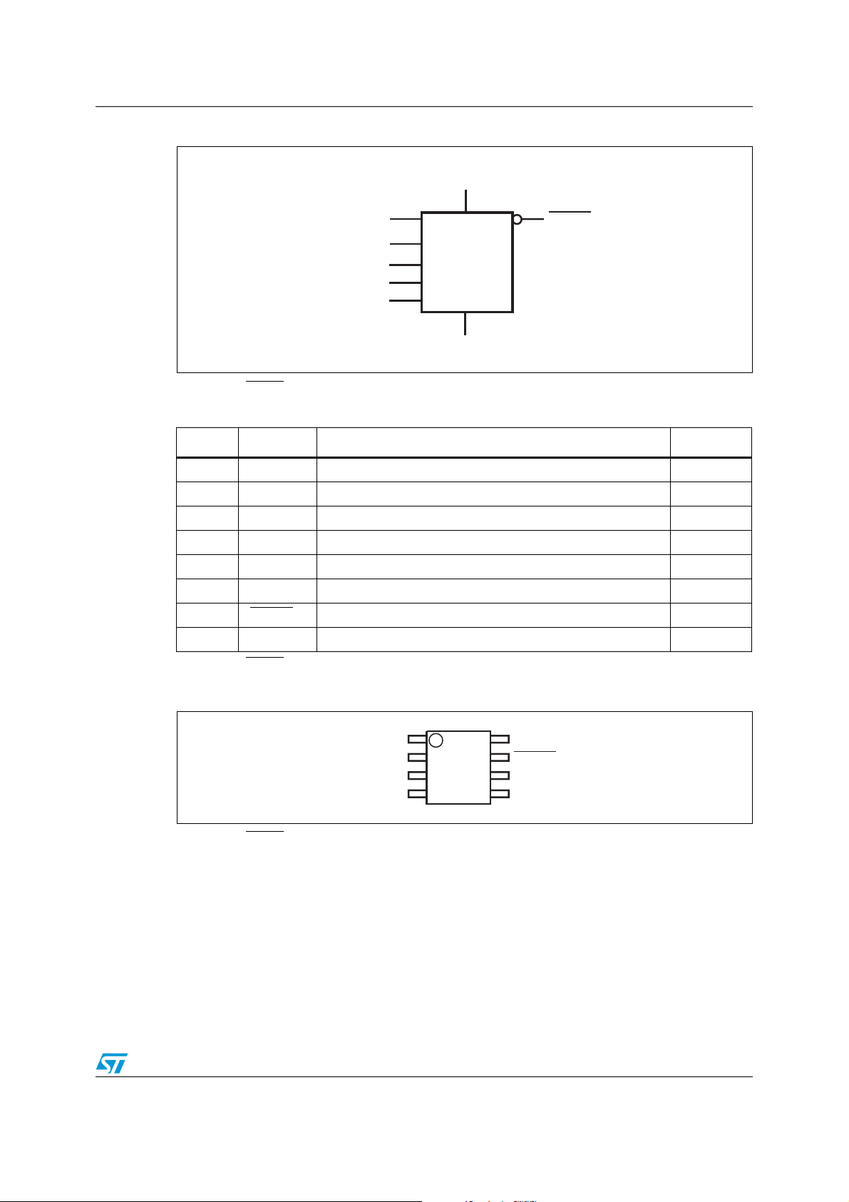
Figure 1. Logic diagram
V
DD
SDA
(1)
EVENT
(1)
SCL
STTS2002
V
SS
1. SDA and EVENT are open drain.
Table 1. Signal names
A
A
A
2
1
0
Pin Symbol Description Direction
1 A0 Serial bus address selection pin. Can be tied to V
2 A1 Serial bus address selection pin. Can be tied to V
3 A2 Serial bus address selection pin. Can be tied to V
4V
SS
5SDA
Supply ground
(1)
Serial data Input/output
or VDD. Input
SS
or VDD. Input
SS
or VDD. Input
SS
6 SCL Serial clock Input
DD
(1)
Event output pin. Open drain and active-low. Output
Supply power (2.3 V to 3.6 V)
7 EVENT
8V
1. SDA and EVENT are open drain.
AI12261
Figure 2. TDFN8 connections (top view)
A0
A1
A2
GND
1. SDA and EVENT are open drain.
Doc ID 17216 Rev 2 3/9
1
2
3
4
V
8
7
6
5
DD
EVENT
SCL
(1)
SDA
(1)
AI12262

Description STTS2002
Figure 3. Block diagram
8
V
DD
2 Kb SPD EEPROM
Standard array
(80h - FFh)
Software
write-protected array
A0
1
A1
2
A2
3
(00h - 7Fh)
Temperature
Sensor
ADC
Capability
Register
Configuration
Register
Temperature
Register
Address Pointer
Register
SMBus/I2C
Interface
Logic Control
Comparator
Timing
Upper
Register
Lower
Register
Critical
Register
Manufacturer
ID
Device ID/
Revision
EVENT
SCL
SDA
7
6
5
V
SS
4
4/9 Doc ID 17216 Rev 2
AI12278a

STTS2002 Temperature sensor registers
2 Temperature sensor registers
The temperature sensor component is comprised of various user-programmable registers.
These registers are required to write their corresponding addresses to the pointer register.
They can be accessed by writing to their respective addresses (see Tab l e 2). Pointer
register bits 7 - 4 must always be written to '0'. This must be maintained, as not setting these
bits to '0' may keep the device from performing to specifications.
The main registers include the :
● Capability register (read-only)
● Configuration register (read/write)
● Temperature register (read-only)
● Temperature trip point registers (read/write), including
– Alarm temperature upper boundary
– Alarm temperature lower boundary and
– Critical temperature
● Manufacturer’s ID register (read-only)
● Device ID and device revision ID register (read-only)
● Temperature resolution register (TRES) (read/write)
Table 2. Temperature sensor registers summary
Address (hex) Register name Power-on default
Not applicable Address pointer Undefined
00 Capability B-grade 0x006F
01 Configuration 0x0000
02 Alarm temperature upper boundary trip 0x0000
03 Alarm temperature lower boundary trip 0x0000
04 Critical temperature trip 0x0000
05 Temperature Undefined
06 Manufacturer’s ID 0x104A
07 Device ID/revision 0x0300
08 Temperature resolution register 0x0001
Doc ID 17216 Rev 2 5/9

Package marking information STTS2002
3 Package marking information
Figure 4. DN package topside marking information (TDFN8)
(1)
B2DN
(2)
TSE2
(3)
xxxx
ai13907b
1. Temperature grade and package
B = B-grade, stacked
2 = Minimum operating voltage of 2.3 V
DN = 0.80 mm TDFN package
2. Device name
TSE2 = STTS2002
3. Traceability codes
6/9 Doc ID 17216 Rev 2

STTS2002 Part numbering
4 Part numbering
Table 3. Ordering information scheme
Example: STTS2002 B 2 DN 3 F
Device
STTS2002
Accuracy grade
B: Maximum accuracy 75 °C to 95 °C = ± 1 °C
Vol tag e
2 = 2.3 V - 3.6 V
Package
DN = TDFN8
Temperature range
3 = –40 °C to 125 °C
Shipping method
®
F = ECOPACK
package, tape & reel packing
For other options, or for more information on any aspect of this device, please contact the
ST sales office nearest you.
Doc ID 17216 Rev 2 7/9

Revision history STTS2002
5 Revision history
Table 4. Document revision history
Date Revision Changes
03-Mar-2010 1 Initial release.
13-Sep-2010 2 Updated Figure 4, Ta b l e 3; minor textual and formatting changes.
8/9 Doc ID 17216 Rev 2

STTS2002
Please Read Carefully:
Information in this document is provided solely in connection with ST products. STMicroelectronics NV and its subsidiaries (“ST”) reserve the
right to make changes, corrections, modifications or improvements, to this document, and the products and services described herein at any
time, without notice.
All ST products are sold pursuant to ST’s terms and conditions of sale.
Purchasers are solely responsible for the choice, selection and use of the ST products and services described herein, and ST assumes no
liability whatsoever relating to the choice, selection or use of the ST products and services described herein.
No license, express or implied, by estoppel or otherwise, to any intellectual property rights is granted under this document. If any part of this
document refers to any third party products or services it shall not be deemed a license grant by ST for the use of such third party products
or services, or any intellectual property contained therein or considered as a warranty covering the use in any manner whatsoever of such
third party products or services or any intellectual property contained therein.
UNLESS OTHERWISE SET FORTH IN ST’S TERMS AND CONDITIONS OF SALE ST DISCLAIMS ANY EXPRESS OR IMPLIED
WARRANTY WITH RESPECT TO THE USE AND/OR SALE OF ST PRODUCTS INCLUDING WITHOUT LIMITATION IMPLIED
WARRANTIES OF MERCHANTABILITY, FITNESS FOR A PARTICULAR PURPOSE (AND THEIR EQUIVALENTS UNDER THE LAWS
OF ANY JURISDICTION), OR INFRINGEMENT OF ANY PATENT, COPYRIGHT OR OTHER INTELLECTUAL PROPERTY RIGHT.
UNLESS EXPRESSLY APPROVED IN WRITING BY AN AUTHORIZED ST REPRESENTATIVE, ST PRODUCTS ARE NOT
RECOMMENDED, AUTHORIZED OR WARRANTED FOR USE IN MILITARY, AIR CRAFT, SPACE, LIFE SAVING, OR LIFE SUSTAINING
APPLICATIONS, NOR IN PRODUCTS OR SYSTEMS WHERE FAILURE OR MALFUNCTION MAY RESULT IN PERSONAL INJURY,
DEATH, OR SEVERE PROPERTY OR ENVIRONMENTAL DAMAGE. ST PRODUCTS WHICH ARE NOT SPECIFIED AS "AUTOMOTIVE
GRADE" MAY ONLY BE USED IN AUTOMOTIVE APPLICATIONS AT USER’S OWN RISK.
Resale of ST products with provisions different from the statements and/or technical features set forth in this document shall immediately void
any warranty granted by ST for the ST product or service described herein and shall not create or extend in any manner whatsoever, any
liability of ST.
ST and the ST logo are trademarks or registered trademarks of ST in various countries.
Information in this document supersedes and replaces all information previously supplied.
The ST logo is a registered trademark of STMicroelectronics. All other names are the property of their respective owners.
© 2010 STMicroelectronics - All rights reserved
STMicroelectronics group of companies
Australia - Belgium - Brazil - Canada - China - Czech Republic - Finland - France - Germany - Hong Kong - India - Israel - Italy - Japan -
Malaysia - Malta - Morocco - Philippines - Singapore - Spain - Sweden - Switzerland - United Kingdom - United States of America
www.st.com
Doc ID 17216 Rev 2 9/9
 Loading...