

Features
STTH4L06
Turbo 2 ultrafast high voltage rectifier
■ Ultrafast switching
■ Low forward voltage drop
■ Low leakage current (platinum doping)
■ High operating junction temperature
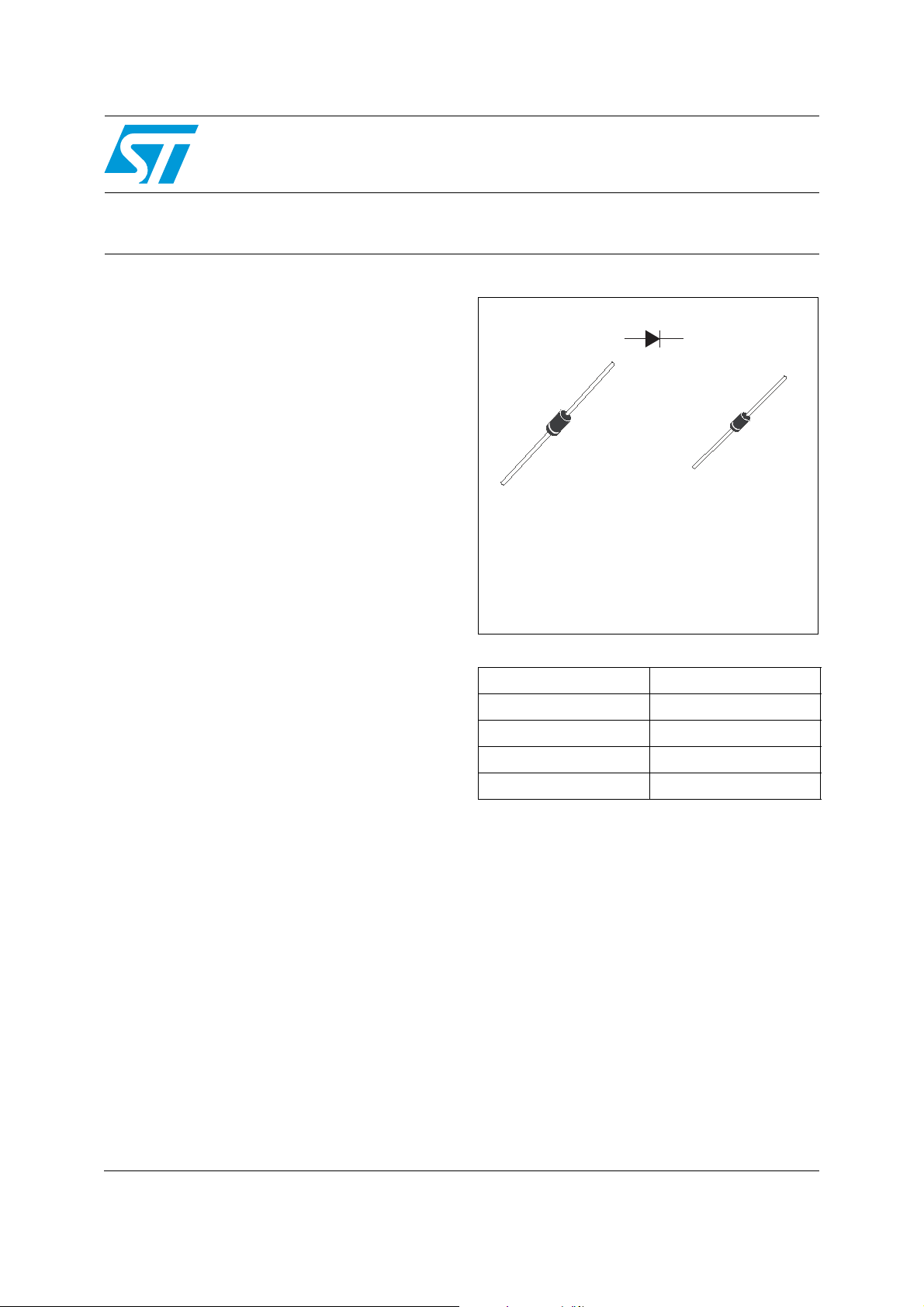
Description
The STTH4L06, which uses ST Turbo 2 600 V
technology, is specially suited as boost diode in
discontinuous or critical mode power factor
corrections.
Packaged in DO-201AD and DO-15, this device is
intended for use as a free wheeling diode in
power supplies and other power switching
applications.
A
K
DO-201AD
STTH4L06
Band indicates cathode
Table 1. Device summary
I
F(AV)
V
RRM
T
j
V
(typ) 0.9 V
F
(typ) 40 ns
t
rr
KA
A
K
DO-15
STTH4L06Q
4 A
600 V
175 °C
September 2009 Doc ID 16276 Rev 1 1/8
www.st.com
8
Characteristics STTH4L06
1 Characteristics
Table 2. Absolute ratings (limiting values at 25 °C unless otherwise specified)
Symbol Parameter Value Unit
V
RRM
I
F(RMS)
I
F(AV)
I
FSM
T
Table 3. Thermal resistance
Repetitive peak reverse voltage 600 V
Forward rms current 10 A
Average forward current 4 A
Surge non repetitive forward current tp = 8.3 ms sinusoidal 80 A
Storage temperature range -65 to + 175 °C
stg
Maximum operating junction temperature 175 °C
T
j
Symbol Parameter Maximum Unit
R
th(j-l)
Junction to lead
Terminal length = 10 mm
R
th(j-a)
Table 4. Static electrical characteristics
Junction to ambient
DO-15 25
DO-201AD 20
DO-15 80
DO-201AD 75
°C/W
°C/W
Symbol Parameter Test conditions Min. Typ. Max. Unit
(1)
I
R
V
F
1. Pulse test: tp = 5 ms, δ < 2%
2. Pulse test: tp = 380 µs, δ < 2%
Reverse leakage current
(2)
Forward voltage drop
= 25 °C
T
j
T
= 150 °C - 15 100
j
T
= 25 °C
j
= 150 °C - 0.85 1.05
j
= 150 °C IF = 4 A - 0.90 1.10
T
j
V
R
I
= 3 A
F
= V
RRM
--3
- - 1.30
µA
VT
To evaluate the maximum conduction losses use the following equation:
P = 0.92 x I
Table 5. Dynamic electrical characteristics
Symbol Parameter
t
Reverse recovery time
rr
I
V
2/8 Doc ID 16276 Rev 1
Reverse recovery current
RM
t
Forward recovery time
fr
Forward recovery voltage IF = 4 A, dIF/dt = 100 A/µs - - 7.5 V
FP
F(AV)
+ 0.045 x I
/dt = -50 A/µs
dI
F
dI
/dt = -100 A/µs - 40 55
F
= 25 °C
T
j
T
= 150 °C - 5 6.5
j
F2(RMS)
Test conditions
I
= 1 A, VR = 30 V
F
IF = 4 A, VR = 400 V,
/dt = -100 A/µs
dI
F
= 4 A, dIF/dt = 100 A/µs,
I
F
VFR = 1.1 x V
Fmax
Min. Typ Max. Unit
-5575
-34
ns
A
--130ns

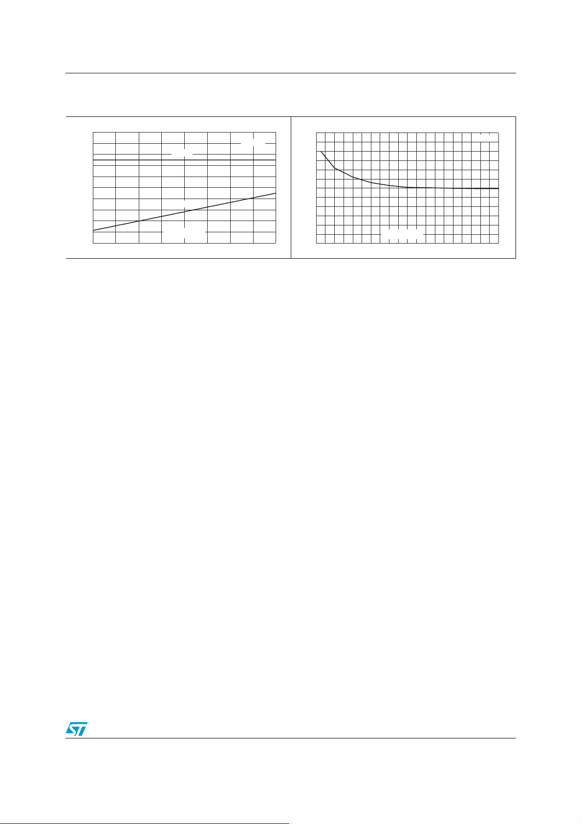
STTH4L06 Characteristics
Figure 1. Conduction losses versus average
current
P(W)
5.5
5.0
4.5
4.0
3.5
3.0
2.5
2.0
1.5
1.0
0.5
0.0
0.0 0.5 1.0 1.5 2.0 2.5 3.0 3.5 4.0 4.5 5.0
δ=0.05
δ=0.1 δ=0.2
I (A)
F(AV)
δ=0.5
δ
=tp/T
δ=1
T
tp
Figure 3. Relative variation of thermal
impedance junction ambient versus
pulse duration (DO-201AD)
Z/R
th(j-a) th(j-a)
1.0
DO-201AD
=10 mm
L
0.9
leads
0.8
0.7
0.6
0.5
0.4
0.3
0.2
Single pulse
0.1
0.0
1.E-01 1.E+00 1.E+01 1.E+02 1.E+03
Epoxy printed circuit FR4
copper thickness = 35 µm
t (s)
p
Figure 5. Peak reverse recovery current
versus dI
I (A)
RM
20
VR=400V
=150 °C
T
18
j
16
14
12
10
8
6
4
2
0
0 50 100 150 200 250 300 350 400 450 500
IF= 0.25 x I
/dt (typical values)
F
IF= 2 x I
IF= I
F(AV)
IF= 0.5 x I
F(AV)
F(AV)
dI /dt(A/µs)
F
F(AV)
Figure 2. Forward voltage drop versus
forward current
I (A)
FM
50
45
40
35
30
25
20
15
10
5
0
0.0 0.5 1.0 1.5 2.0 2.5
Tj=150°C
Tj=150°C
(Typical values)
(Typical values)
Tj=150°C
Tj=150°C
(Maximum values)
(Maximum values)
Tj=25°C
(Maximum values)
V (V)
FM
Figure 4. Relative variation of thermal
impedance junction ambient versus
pulse duration (DO-15)
Z/R
th(j-a) th(j-a)
1.0
DO-15
L
0.9
0.8
0.7
0.6
0.5
0.4
0.3
0.2
0.1
0.0
=10 mm
leads
Single pulse
1.E-01 1.E+00 1.E+01 1.E+02 1.E+03
Epoxy printed circuit FR4
copper thickness = 35 µm
t (s)
p
Figure 6. Reverse recovery time versus dI
(typical values)
t (ns)
rr
500
450
400
350
300
250
200
150
100
50
0
0 20 40 60 80 100 120 140 160 180 200
IF= 0.5 x I
F(AV)
dI /dt(A/µs)
F
IF= I
F(AV)
IF= 2 x I
VR=400V
=150 °C
T
j
F(AV)
F
/dt
Doc ID 16276 Rev 1 3/8

Characteristics STTH4L06
Figure 7. Reverse recovery charges versus
dI
/dt (typical values)
F
Figure 8. Relative variations of dynamic
parameters versus junction
temperature
Q (nC)
rr
600
VR=400V
550
=150 °C
T
j
500
450
400
350
300
250
200
150
100
50
0
0 20 40 60 80 100 120 140 160 180 200
IF= 2 x I
IF= I
IF= 0.5 x I
dI /dt(A/µs)
F
F(AV)
F(AV)
F(AV)
1.0
0.9
0.8
0.7
0.6
0.5
0.4
0.3
0.2
0.1
0.0
25 50 75 100 125
I
RM
Q
rr
IF=I
F(AV)
T (°C)
j
VR=400V
Reference: T
j
=150 °C
Figure 9. Transient peak forward voltage
versus dI
V (V)
FP
10
IF=I
F(AV)
Tj=125°C
9
8
7
6
5
4
3
2
1
0
0 20 40 60 80 100 120 140 160 180 200
/dt (typical values)
F
dI /dt(A/µs)
F
Figure 11. Junction capacitance versus
reverse voltage applied
(typical values)
C(pF)
100
10
V (V)
1
1 10 100 1000
R
V
F=1MHz
osc
Tj=25°C
=30mV
RMS
Figure 10. Forward recovery time versus dI
(typical values)
t (ns)
fr
450
400
350
300
250
200
150
100
50
0
0 20 40 60 80 100 120 140 160 180 200
dI /dt(A/µs)
F
IF=I
F(AV)
VFR=1.1 x VFmax.
=125°C
T
j
Figure 12. Thermal resistance junction to
ambient versus copper surface
under lead (DO-201AD)
R (°C/W)
th(j-a)
80
70
60
50
40
30
20
10
0
0.0 0.5 1.0 1.5 2.0 2.5 3.0 3.5 4.0 4.5 5.0
Epoxy printed circuit FR4
copper thickness = 35 µm
S (cm²)
CU
DO-201AD
F
/dt
4/8 Doc ID 16276 Rev 1
STTH4L06 Characteristics
Figure 13. Thermal resistance versus lead length
(DO-201AD)
R (°C/W)
th
100
90
80
70
60
50
40
30
20
10
0
5 10152025
R
th(j-a)
R
th(j-l)
L (mm)
lead
DO-201AD
Figure 14. Thermal resistance versus lead length
(DO-15)
R (°C/W)
th(j-a)
120
100
80
60
40
20
0
0.0 0.5 1.0 1.5 2.0 2.5 3.0 3.5 4.0 4.5 5.0
L (mm)
lead
DO-15
Doc ID 16276 Rev 1 5/8

Package information STTH4L06
2 Package information
■ Epoxy meets UL94, V0
■ Band indicates cathode
■ Bending method: see application note AN1471
In order to meet environmental requirements, ST offers these devices in different grades of
ECOPACK
specifications, grade definitions and product status are available at: www.st.com.
ECOPACK
Table 6. DO-15 dimensions
®
packages, depending on their level of environmental compliance. ECOPACK®
®
is an ST trademark.
Dimensions
CC
A
Ref.
Millimeters Inches
Min. Max. Min. Max.
A 6.05 6.75 0.238 0.266
D
B
B 2.95 3.53 0.116 0.139
C 26 31 1.024 1.220
D 0.71 0.88 0.028 0.035
Table 7. DO-201AD dimensions
Dimensions
Ref.
Millimeters Inches
Min. Max. Min. Max.
BB
Note 1 Note 1
A
EE
A 9.50 0.374
B 25.40 1.000
ØD
ØC
Note 2
C 5.30 0.209
D 1.30 0.051
E 1.25 0.049
Notes 1 - The lead diameter ø D is not
6/8 Doc ID 16276 Rev 1
controlled over zone E
2 - The minimum length which must stay
straight between the right angles after
bending is 0.59"(15mm)
STTH4L06 Ordering information
3 Ordering information
Table 8. Ordering information
Order code Marking Package Weight Base qty Delivery mode
STTH4L06 STTH4L06 DO-201AD 1.16 g 600 Ammopack
STTH4L06RL STTH4L06 DO-201AD 1.16 g 1900 Tape andreel
STTH4L06Q STTHLO6Q DO-15 0.4 g 600 Ammopack
STTH4L06QRL STTHLO6Q DO-15 0.4 g 1900 Tape and reel
4 Revision history
Table 9. Document revision history
Date Revision Changes
22-Sep-2009 1 First issue
Doc ID 16276 Rev 1 7/8

STTH4L06
Please Read Carefully:
Information in this document is provided solely in connection with ST products. STMicroelectronics NV and its subsidiaries (“ST”) reserve the
right to make changes, corrections, modifications or improvements, to this document, and the products and services described herein at any
time, without notice.
All ST products are sold pursuant to ST’s terms and conditions of sale.
Purchasers are solely responsible for the choice, selection and use of the ST products and services described herein, and ST assumes no
liability whatsoever relating to the choice, selection or use of the ST products and services described herein.
No license, express or implied, by estoppel or otherwise, to any intellectual property rights is granted under this document. If any part of this
document refers to any third party products or services it shall not be deemed a license grant by ST for the use of such third party products
or services, or any intellectual property contained therein or considered as a warranty covering the use in any manner whatsoever of such
third party products or services or any intellectual property contained therein.
UNLESS OTHERWISE SET FORTH IN ST’S TERMS AND CONDITIONS OF SALE ST DISCLAIMS ANY EXPRESS OR IMPLIED
WARRANTY WITH RESPECT TO THE USE AND/OR SALE OF ST PRODUCTS INCLUDING WITHOUT LIMITATION IMPLIED
WARRANTIES OF MERCHANTABILITY, FITNESS FOR A PARTICULAR PURPOSE (AND THEIR EQUIVALENTS UNDER THE LAWS
OF ANY JURISDICTION), OR INFRINGEMENT OF ANY PATENT, COPYRIGHT OR OTHER INTELLECTUAL PROPERTY RIGHT.
UNLESS EXPRESSLY APPROVED IN WRITING BY AN AUTHORIZED ST REPRESENTATIVE, ST PRODUCTS ARE NOT
RECOMMENDED, AUTHORIZED OR WARRANTED FOR USE IN MILITARY, AIR CRAFT, SPACE, LIFE SAVING, OR LIFE SUSTAINING
APPLICATIONS, NOR IN PRODUCTS OR SYSTEMS WHERE FAILURE OR MALFUNCTION MAY RESULT IN PERSONAL INJURY,
DEATH, OR SEVERE PROPERTY OR ENVIRONMENTAL DAMAGE. ST PRODUCTS WHICH ARE NOT SPECIFIED AS "AUTOMOTIVE
GRADE" MAY ONLY BE USED IN AUTOMOTIVE APPLICATIONS AT USER’S OWN RISK.
Resale of ST products with provisions different from the statements and/or technical features set forth in this document shall immediately void
any warranty granted by ST for the ST product or service described herein and shall not create or extend in any manner whatsoever, any
liability of ST.
ST and the ST logo are trademarks or registered trademarks of ST in various countries.
Information in this document supersedes and replaces all information previously supplied.
The ST logo is a registered trademark of STMicroelectronics. All other names are the property of their respective owners.
© 2009 STMicroelectronics - All rights reserved
STMicroelectronics group of companies
Australia - Belgium - Brazil - Canada - China - Czech Republic - Finland - France - Germany - Hong Kong - India - Israel - Italy - Japan -
Malaysia - Malta - Morocco - Philippines - Singapore - Spain - Sweden - Switzerland - United Kingdom - United States of America
www.st.com
8/8 Doc ID 16276 Rev 1
 Loading...