

ST STTH30W03C User Manual

Features
■ Ultrafast switching
■ Low reverse recovery current
■ Low thermal resistance
■ Reduces switching losses
■ ECOPACK
®
2 compliant component
STTH30W03C
Turbo 2 ultrafast high voltage rectifier
Datasheet − production data
A1
K
A2
Description
The STTH30W03C uses ST Turbo 2 300 V
technology. It is especially suited to be used for
DC/DC and DC/AC converters in secondary stage
of MIG/MMA/TIG welding machine. Housed in
ST's TO-247, this device offers high power
integration for all welding machines and industrial
applications.
A1
TO-247
STTH30W03CW
Table 1. Device summary
Symbol Value
I
F(AV)
V
RRM
(typ) 20 ns
t
rr
T
j
V
(typ) 0.90 V
F
A2
K
2 x 15 A
300 V
175 °C
May 2012 Doc ID 023116 Rev 1 1/8
This is information on a product in full production.
www.st.com
8

Characteristics STTH30W03C
1 Characteristics
Table 2. Absolute ratings (limiting values, at 25 °C, unless otherwise specified)
Symbol Parameter Value Unit
V
I
F(RMS)
I
F(AV)
I
FSM
T
Table 3. Thermal resistance
Symbol Parameter Value Unit
Repetitive peak reverse voltage 300 V
RRM
RMS forward current 30 A
= 140 °C Per diode 15
T
Average forward current, δ = 0.5
c
T
= 130 °C Per device 30
c
Surge non repetitive forward current tp = 10 ms sinusoidal 150 A
Storage temperature range -65 to + 175 °C
stg
Maximum operating junction temperature + 175 °C
T
j
A
R
R
Junction to case
th(j-c)
Coupling 0.3
th(c)
Total
1.0
°C / W
When diodes 1 and 2 are used simultaneously:
Per diode 1.7
T
j(diode 1)
Table 4. Static electrical characteristics
Symbol Parameter Test conditions Min. Typ Max. Unit
1. Pulse test: tp = 5 ms, δ < 2%
2. Pulse test: tp = 380 µs, δ < 2%
IR
V
= P
(diode 1)
(1)
Reverse leakage current
(2)
Forward voltage drop
F
x R
(Per diode) + P
th(j-c)
VR = V
= 15A
I
F
= 30 A
I
F
x R
RRM
th(c)
(diode 2)
T
= 25 °C
j
= 125 °C 10 100
T
j
= 25 °C
T
j
T
= 150 °C 0.90 1.10
j
= 25 °C
T
j
T
= 150 °C 1.1 1.35
j
10
1.40
1.6
To evaluate the conduction losses use the following equation:
P = 0.85 x I
+ 0.0167 I
F(AV)
F2(RMS)
µA
V
2/8 Doc ID 023116 Rev 1
STTH30W03C Characteristics
Table 5. Dynamic electrical characteristics
Symbol Parameter Test conditions Min. Typ Max. Unit
Q
S
I
RM
factor
t
V
Reverse recovery current
Reverse recovery charge 160 nC
RR
= 125 °C
T
j
Softness factor 0.3
Reverse recovery time Tj = 25 °C
rr
t
Forward recovery time Tj = 25 °C
fr
Forward recovery voltage Tj = 25 °C 2.0 3.0 V
FP
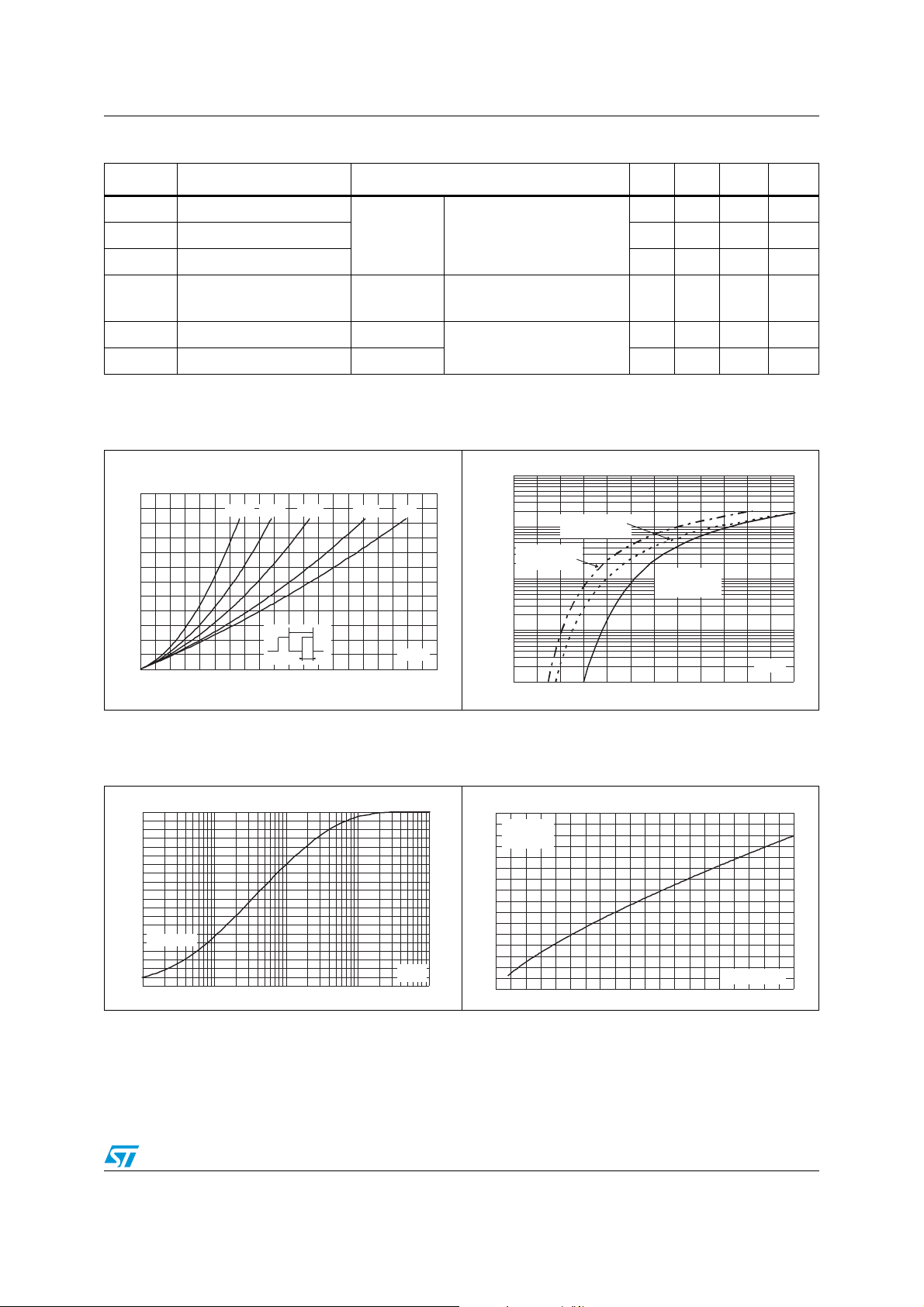
Figure 1. Average forward power dissipation
versus average forward current
IF = 15 A, VR = 200 V
dIF/dt = -200 A/µs
IF = 1 A, VR = 30 V
dIF/dt = -100 A/µs
IF = 15 A, VFR = 1.2 V
/dt = 100 A/µs
dI
F
Figure 2. Forward voltage drop versus
forward current (per diode)
79 A
20 25 ns
230 ns
(per diode)
IFM(A)
P(W)
F(AV)
24
20
δ = 0.05
16
12
8
4
0
02468101214161820
δ1= 0.
δ
= tp/T
δ = 0.2
T
tp
δ = 0.5
δ = 1
I
F(AV)
(A)
1000.0
100.0
Tj=150 °C
(Typical values)
10.0
1.0
0.1
0.0 0.5 1.0 1.5 2.0 2.5 3.0
Tj=150°C
(Maximum values)
T
°C
= 25
j
(Maximum values)
VFM(V)
Figure 3. Relative variation of thermal
impedance junction to case versus
pulse duration
Z
th(j-c)/Rth(j-c)
1.0
0.9
0.8
0.7
0.6
0.5
0.4
0.3
Single pulse
0.2
0.1
0.0
1.E-04 1.E-03 1.E-02 1.E-01 1.E+00
Figure 4. Peak reverse recovery current
versus dI
/dt (typical values, per
F
diode)
IRM(A)
16
IF=I
F(AV)
VR=200 V
14
T
=125 °C
j
12
10
8
6
4
tp(s)
Doc ID 023116 Rev 1 3/8
2
0
0 50 100 150 200 250 300 350 400 450 500
dIF/dt(A/µs)
 Loading...