


Features
■ very low conduction losses
■ negligible switching losses
■ low forward and reverse recovery times
■ high junction temperature
■ AEC-Q101 qualified
STTH2R02-Y
Automotive ultrafast recovery diode
KA
A
Description
The STTH2R02 uses ST's new 200 V planar Pt
doping technology, and it is specially suited for
switching mode base drive and transistor circuits.
Packaged in SMB, this device is intended for use
in low voltage, high frequency inverters, free
wheeling and polarity protection for automotive
applications.
K
SMB
STTH2R02UY
Table 1. Device summary
Symbol Value
I
F(AV)
V
RRM
T
(max) 175 °C
j
(typ) 0.7 V
V
F
(typ) 15 ns
t
rr
2 A
200 V
October 2010 Doc ID 17934 Rev 1 1/8
www.st.com
8

Characteristics STTH2R02-Y
1 Characteristics
Table 2. Absolute ratings (limiting values at T
Symbol Parameter Value Unit
= 25 °C, unless otherwise specified)
j
V
RRM
I
FRM
I
F(RMS)
I
F(AV)
I
FSM
T
T
Table 3. Thermal parameters
Repetitive peak reverse voltage 200 V
= 5 µs, F = 5 kHz
Repetitive peak forward current
t
p
Forward rms current 60 A
Average forward current, δ = 0.5 Tc = 90 °C 2 A
= 10 ms Sinusoidal
Surge non repetitive forward current
Storage temperature range -65 to +175 °C
stg
Operating junction temperature range -40 to +175 °C
j
t
p
60 A
75 A
Symbol Parameter Value Unit
R
th(j-c)
Table 4. Static electrical characteristics
Junction to case 30 °C/W
Symbol Parameter Test conditions Min. Typ. Max. Unit
T
(1)
I
R
V
1. Pulse test: tp = 5 ms, δ < 2 %
2. Pulse test: tp = 380 µs, δ < 2 %
Reverse leakage current
(2)
Forward voltage drop
F
= 25 °C
j
= 125 °C - 2 20
T
j
= 25 °C IF = 6 A - - 1.20
T
j
T
= 25 °C
j
Tj = 100 °C - 0.76 0.85
= 150 °C - 0.70 0.80
T
j
V
R
I
= 2 A
F
= V
RRM
--3
- 0.89 1.0
µA
V
To evaluate the conduction losses use the following equation:
P = 0.68 x I
2/8 Doc ID 17934 Rev 1
F(AV)
+ 0.06 I
F2(RMS)
STTH2R02-Y Characteristics
Table 5. Dynamic characteristics
Symbol Parameter
t
rr
I
RM
t
fr
V
FP
Reverse recovery time
Reverse recovery current
Forward recovery time
Forward recovery voltage
Test conditions
I
= 1 A, dIF/dt = -50 A/µs,
F
VR = 30 V, Tj = 25 °C
= 1 A, dIF/dt = -100 A/µs,
I
F
VR = 30 V, Tj = 25 °C
IF = 2 A, dIF/dt = -200 A/µs,
VR = 160 V, Tj = 125 °C
IF = 2 A, dIF/dt = 100 A/µs
VFR = 1.1 x V
= 2 A, dIF/dt = 100 A/µs,
I
F
= 25 °C
T
j
, Tj = 25 °C
Fmax
Min. Typ Max. Unit
-2330
-1520
-34A
-40- ns
-2.0- V
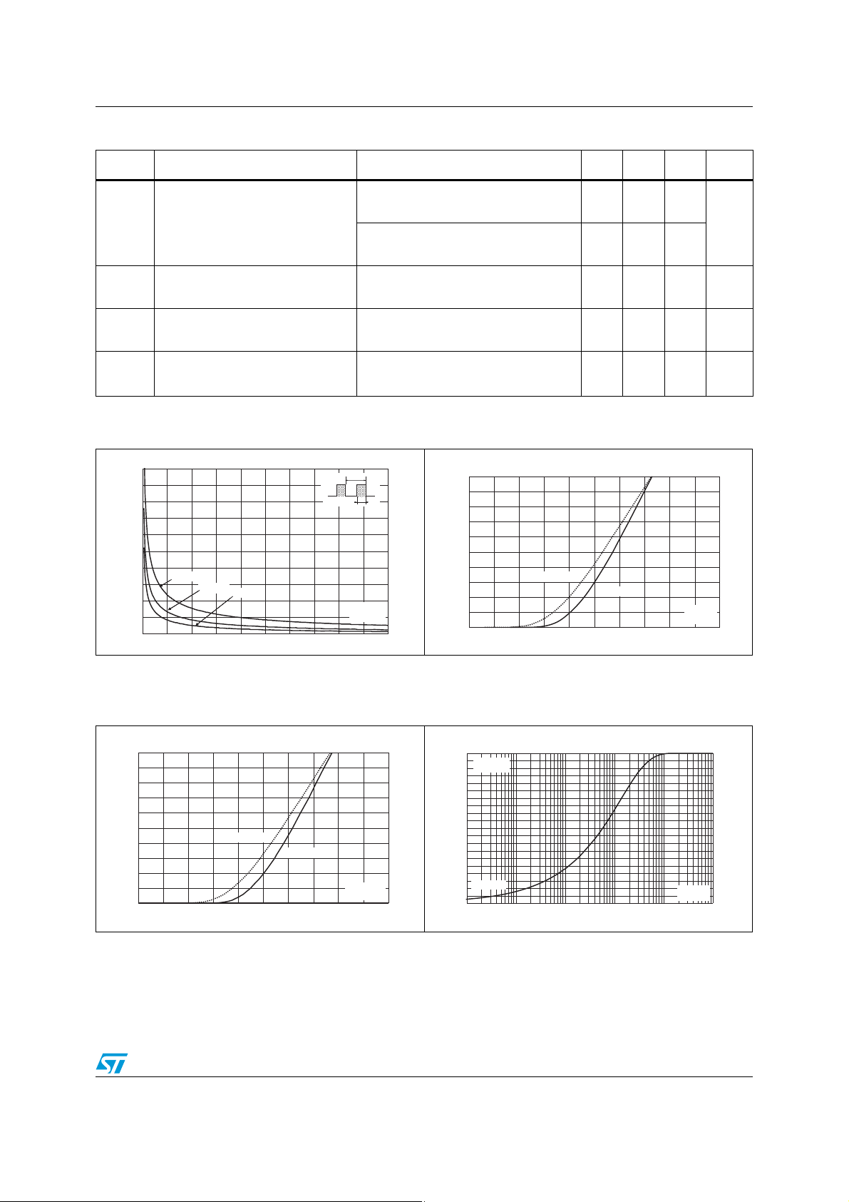
Figure 1. Peak current versus duty cycle Figure 2. Forward voltage drop versus
forward current (typical values)
100
IM(A)
T
T
I
I
M
M
80
60
d
δ
=tp/T
=tp/T
tp
tp
IFM(A)
50
40
30
ns
40
20
P = 5 WP = 5 W
P = 2 WP = 2 W
P = 1 WP = 1 W
δ
0
0.0 0.1 0.2 0.3 0.4 0.5 0.6 0.7 0.8 0.9 1.0
Figure 3. Forward voltage drop versus
forward current (maximum values)
IFM(A)
50
40
30
20
10
0
0.0 0.5 1.0 1.5 2.0 2.5
Tj=150°C
Tj=25°C
VFM(V)
20
10
0
0.0 0.5 1.0 1.5 2.0 2.5
Tj=150°C
Tj=25°C
VFM(V)
Figure 4. Relative variation of thermal
impedance junction to case versus
pulse duration
Z
th(j-a)/Rth(j-a)
1.0
SMA
S
=1cm²
0.9
cu
0.8
0.7
0.6
0.5
0.4
0.3
0.2
Single pulse
0.1
0.0
1.E-02 1.E-01 1.E+00 1.E+01 1.E+02 1.E+03
tP(ms)
Doc ID 17934 Rev 1 3/8
 Loading...