

Main product characteristics
STTH2R02
Ultrafast recovery diode
I
F(AV)
V
RRM
T
(max) 175° C
j
(typ) 0.7 V
V
F
(typ) 15 ns
t
rr
2 A
200 V
Features and benefits
■ Very low conduction losses
■ Negligible switching losses
■ Low forward and reverse recovery times
■ High junction temperature
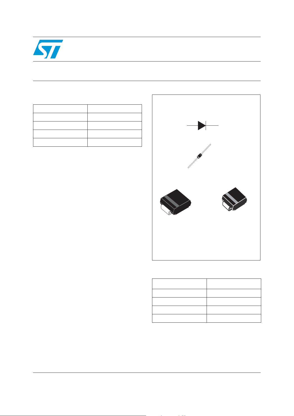
Description
The STTH2R02 uses ST's new 200 V planar Pt
doping technology, and it is specially suited for
switching mode base drive and transistor circuits.
Packaged in DO-15, SMA, and SMB, this device
is intended for use in low voltage, high frequency
inverters, free wheeling and polarity protection.
K
K
SMA
STTH2R02A
STTH2R02Q
A
KA
A
DO-15
A
K
SMB
STTH2R02U
Order codes
Part Number Marking
STTH2R02Q STTH2R02
STTH2R02QRL STTH2R02
STTH2R02A R2A
STTH2R02U R2U
October 2006 Rev 2 1/9
www.st.com
Characteristics STTH2R02
1 Characteristics
Table 1. Absolute ratings (limiting values at T
= 25° C, unless otherwise specified)
j
Symbol Parameter Value Unit
V
I
RRM
FRM
Repetitive peak reverse voltage 200 V
(1)
Repetitive peak forward current
DO-15
tp = 5 µs, F = 5 kHz
60 A
SMA, SMB
DO-15
I
F(RMS)
I
F(AV)
I
FSM
T
1. On infinite heatsink with 10 mm lead length
Table 2. Thermal parameters
RMS forward current
SMA, SMB
Average forward current, δ = 0.5
DO-15 T
SMA, SMB T
= 90° C
lead
= 90° C
c
Surge non repetitive forward current tp = 10 ms Sinusoidal 75 A
Storage temperature range -65 to + 175 ° C
stg
Maximum operating junction temperature 175 ° C
T
j
60 A
2A
Symbol Parameter Value Unit
Junction to lead Lead Length = 10 mm on infinite heatsink DO-15 45
R
th(j-c)
Junction to case SMA, SMB 30
° C/W
Table 3. Static electrical characteristics
Symbol Parameter Test conditions Min. Typ Max. Unit
(1)
I
R
V
1. Pulse test: tp = 5 ms, δ < 2 %
2. Pulse test: t
Reverse leakage current
(2)
Forward voltage drop
F
= 380 µs, δ < 2 %
p
= 25° C
j
= 125° C 2 20
T
j
= 25° C IF = 6 A 1.20
T
j
T
= 25° C
j
Tj = 100° C 0.76 0.85
= 150° C 0.70 0.80
T
j
V
R
= 2 A
I
F
= V
RRM
0.89 1.0
3
T
To evaluate the conduction losses use the following equation:
P = 0.68 x I
F(AV)
+ 0.06 I
F2(RMS)
µA
V
2/9
STTH2R02 Characteristics
Table 4. Dynamic characteristics
Symbol Parameter
t
rr
I
RM
t
fr
V
FP
Reverse recovery time
Reverse recovery current
Forward recovery time
Forward recovery voltage
Test conditions
I
= 1 A, dIF/dt = -50 A/µs,
F
VR = 30 V, Tj = 25° C
= 1 A, dIF/dt = -100 A/µs,
I
F
= 30 V, Tj = 25° C
V
R
= 2 A, dIF/dt = -200 A/µs,
I
F
VR = 160 V, Tj = 125° C
I
= 2 A, dIF/dt = 100 A/µs
F
VFR = 1.1 x V
, Tj = 25° C
Fmax
IF = 2 A, dIF/dt = 100 A/µs,
= 25° C
T
j
Min. Typ Max. Unit
23 30
15 20
34 A
40 ns
2.0 V
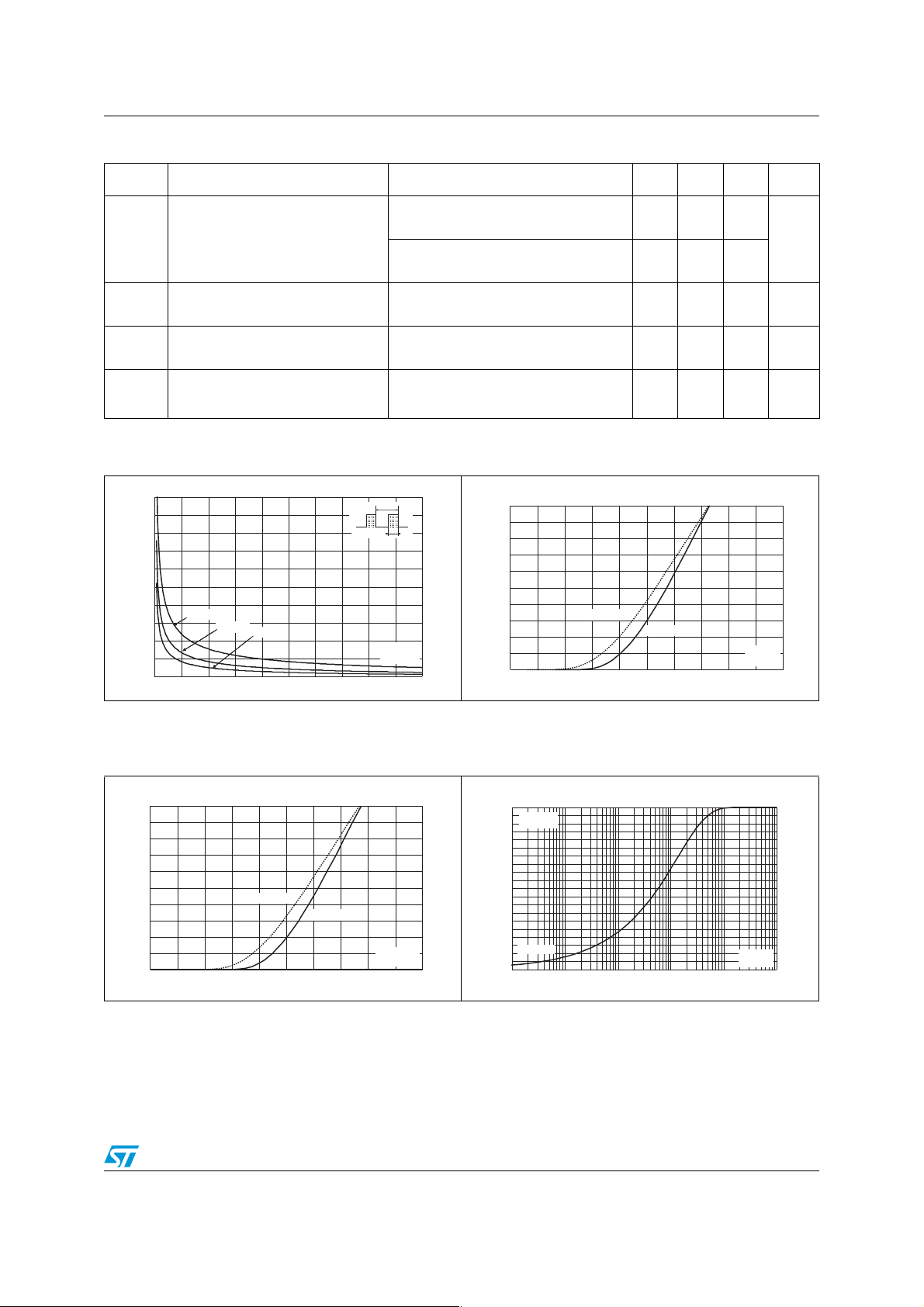
Figure 1. Peak current versus duty cycle Figure 2. Forward voltage drop versus
forward current (typical values)
100
IM(A)
T
T
I
I
M
M
80
60
d
δ
=tp/T
=tp/T
tp
tp
IFM(A)
50
40
30
ns
40
20
P = 5 WP = 5 W
P = 2 WP = 2 W
P = 1 WP = 1 W
δ
0
0.0 0.1 0.2 0.3 0.4 0.5 0.6 0.7 0.8 0.9 1.0
Figure 3. Forward voltage drop versus
forward current (maximum values)
IFM(A)
50
40
30
20
10
0
0.0 0.5 1.0 1.5 2.0 2.5
Tj=150°C
Tj=25°C
VFM(V)
20
10
0
0.0 0.5 1.0 1.5 2.0 2.5
Tj=150°C
Tj=25°C
VFM(V)
Figure 4. Relative variation of thermal
impedance junction to case versus
pulse duration (SMA)
Z
th(j-a)/Rth(j-a)
1.0
SMA
S
=1cm²
0.9
cu
0.8
0.7
0.6
0.5
0.4
0.3
0.2
Single pulse
0.1
0.0
1.E-02 1.E-01 1.E+00 1.E+01 1.E+02 1.E+03
tP(s)
3/9
 Loading...