

ST STTH2L06 User Manual
STTH2L06
High efficiency ultrafast diode
Features
■ Very low conduction losses
■ Negligible switching losses
■ Low forward and reverse recovery times
■ High junction temperature
Description
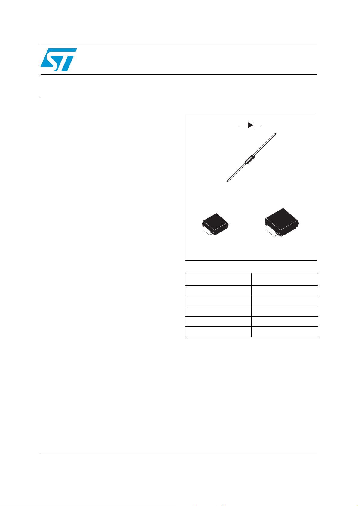
The STTH2L06 is using ST Turbo 2 600 V planar
Pt doping technology. It is specially suited for
SMPS and base drive transistor circuits.
Packaged in axial, SMA and SMB, this device is
intended for use in high frequency inverters, free
wheeling and polarity protection.
DO-41
STTH2L06
SMA
STTH2L06A
Table 1. Device summary
Symbol Value
I
F(AV)
V
RRM
T
j
(typ) 0.85 V
V
F
t
(max) 60 ns
rr
KA
SMB
STTH2L06U
2 A
600 V
175 °C
October 2009 Doc ID10758 Rev 2 1/9
www.st.com
9
Characteristics STTH2L06
1 Characteristics
Table 2. Absolute ratings (limiting values)
Symbol Parameter Value Unit
V
I
F(RMS)
I
F(AV)
I
T
Table 3. Thermal resistance
Repetitive peak reverse voltage 600 V
RRM
Forward rms current 7 A
DO-41 T
Average forward current, δ = 0.5
SMB T
DO-41
Surge non repetitive forward current
FSM
Storage temperature range -65 to + 175 °C
stg
Maximum operating junction temperature 175 °C
T
j
SMA / SMB 35
= 90 °C 2
l
= 100 °C 2
l
= 115 °C 2
l
t
= 10 ms
p
sinusoidal
45
Symbol Parameter Maximum Unit
DO-41 L = 5 mm 35
R
Junction to lead
th(j-l)
°C/WSMA 30
SMB 25
Table 4. Static electrical characteristics
Symbol Parameter Test conditions Min. Typ. Max. Unit
Reverse leakage
(1)
I
R
current
(2)
V
1. Pulse test: tp = 5 ms, δ < 2 %
2. Pulse test: tp = 380 µs, δ < 2 %
Forward voltage drop
F
= 25 °C
T
j
= 150 °C 12 85
T
j
T
= 25 °C
j
= 150 °C 0.85 1.05
T
j
VR = V
= 2 A
I
F
RRM
2
1.3
ASMA T
A
µA
V
To evaluate the maximum conduction losses use the following equation:
P = 0.89 x I
2/9 Doc ID10758 Rev 2
F(AV)
+ 0.08 I
F2(RMS)
STTH2L06 Characteristics
Table 5. Dynamic electrical characteristics
Symbol Parameter
t
Reverse recovery time Tj = 25 °C
rr
t
Forward recovery time
fr
Tj = 25 °C
V
Forward recovery voltage 9 V
FP
Figure 1. Conduction losses vs average
forward current
P(W)
2.5
2.0
1.5
1.0
0.5
0.0
0.00 0.25 0.50 0.75 1.00 1.25 1.50 1.75 2.00 2.25
δ = 0.05
δ = 0.1
I (A)
F(AV)
δ = 0.2
δ = 0.5
Figure 3. Relative variation of thermal
impedance junction to case vs
pulse duration (SMA - S
Z/R
th(j-a) th(j-a)
1.0
0.9
0.8
0.7
0.6
0.5
0.4
0.3
0.2
Single pulse
0.1
0.0
1.E-02 1.E-01 1.E+00 1.E+01 1.E+02 1.E+03
t (s)
p
Test conditions
δ = 1
T
=tp/T
δ
= 1 cm2)
CU
Min. Typ. Max. Unit
IF = 1 A,
dIF/dt = 50 A/µs,
60 85 ns
VR = 30 V
IF = 2 A
dIF/dt = 100 A/µs
VFR = 1.1 x V
Fmax
Figure 2. Forward voltage drop vs
forward current
I (A)
FM
10
9
8
7
6
5
4
3
2
tp
1
0
0.0 0.1 0.2 0.3 0.4 0.5 0.6 0.7 0.8 0.9 1.0 1.1 1.2 1.3 1.4 1.5 1.6 1.7 1.8 1.9 2.0
(maximum values)
T =150°C
j
(typical values)
T =150°C
j
Figure 4. Relative variation of thermal
impedance junction to case vs
pulse duration (SMB - SCU = 1 cm2)
Z/R
th(j-a) th(j-a)
1.0
0.9
0.8
0.7
0.6
0.5
0.4
0.3
0.2
Single pulse
0.1
0.0
1.E-03 1.E-02 1.E-01 1.E+00 1.E+01 1.E+02 1.E+03
t (s)
p
V (V)
FM
100 ns
T =25°C
j
(maximum values)
Doc ID10758 Rev 2 3/9
 Loading...