

ST STTH212 User Manual
STTH212
High voltage ultrafast diode
Main product characteristics
I
F(AV)
V
V
F
t
(max)
rr
RRM
T
j
(typ)
2 A
1200 V
175°C
1.0 V
75 ns
Features and benefits
■ Low forward voltage drop
■ High reliability
■ High surge current capability
■ Soft switching for reduced EMI disturbances
■ Planar technology
Description
The STTH212, which is using ST ultrafast high
voltage planar technology, is specially suited for
free-wheeling, clamping, snubbering,
demagnetization in power supplies and other
power switching applications.
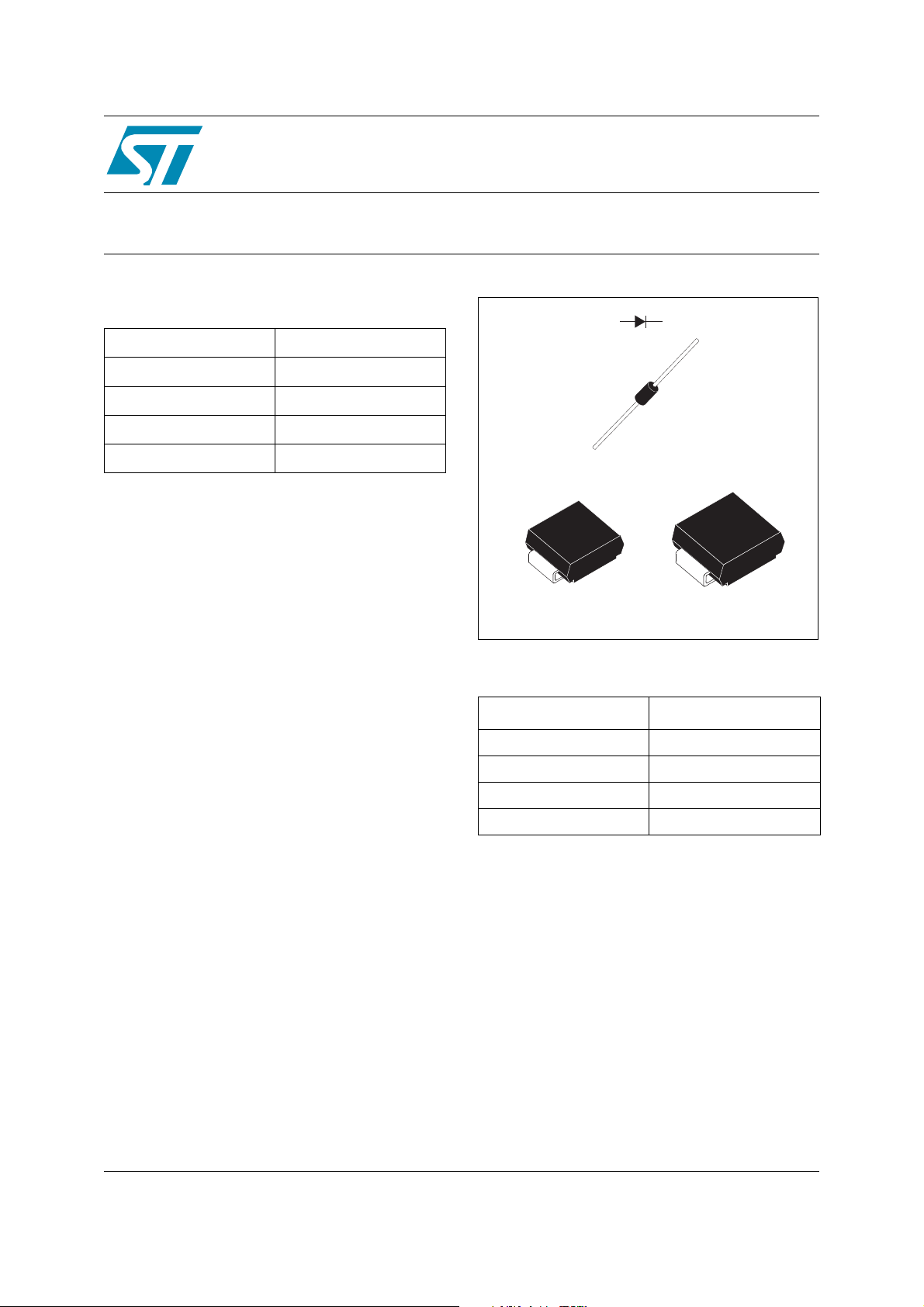
Housed in axial, SMB, and SMC packages, this
diode will reduce the losses in high switching
freqency operations.
DO-201AD
STTH212
SMB
STTH212U
Order codes
Part Number Marking
STTH212 STTH212
STTH212RL STTH212
STTH212U U22
STTH212S S12
KA
SMC
STTH212S
Rev 1
June 2005 1/9
www.st.com
9
1 Electrical characteristics STTH212
1 Electrical characteristics
Table 1. Absolute Ratings (limiting values)
Symbol Parameter Value Unit
V
RRM
V
(RMS)
I
F(AV)
I
F(RMS)
I
FSM
T
Repetitive peak reverse voltage 1200 V
RMS voltage 850 V
= 105°C
DO-201AD
Average forward current
δ = 0.5
SMC
T
l
= 90°C
T
l
Tl = 105°C
RMS forward current DO-201AD, SMB, SMC 10 A
Forward surge current tp = 8.3ms
Storage temperature range -50 to + 175 °C
stg
T
Maximum operating junction temperature 175 °C
j
DO-201AD, SMB, SMC 40 A
2ASMB
Table 2. Thermal parameters
Symbol Parameter Value Unit
L = 10 mm DO-201AD 20
R
th(j-l)
Junction to lead
SMC 20
R
th(j-a)
Junction to ambient L = 10 mm DO-201AD 75 °C/W
Table 3. Static Electrical Characteristics
°C/WSMB 25
Symbol Parameter Test conditions Min. Typ Max. Unit
= 25°C
T
I
Reverse leakage current
R
j
= 125°C
T
j
= V
V
R
RRM
Tj = 25°C
V
Forward voltage drop
F
= 125°C
T
j
T
= 150°C
j
I
F
= 2A
To evaluate the conduction losses use the following equation: P = 1.26 x I
1.07 1.50
1.0 -
F(AV)
10
100
1.75
+ 0.12 I
F2(RMS)
2/9
µA
V
STTH212 1 Electrical characteristics
Table 4. Dynamic Electrical Characteristics
Symbol Parameter Test conditions Min. Typ Max. Unit
t
Reverse recovery
rr
time
Forward recovery
t
fr
time
V
Forward recovery
FP
voltage
Tj = 25°C IF = 1A dIF/dt = -100 A/µs VR =30V
I
= 2A dIF/dt = 50 A/µs
Tj = 25°C
F
VFR = 1.1 x V
Fmax
75 ns
500 ns
30 V
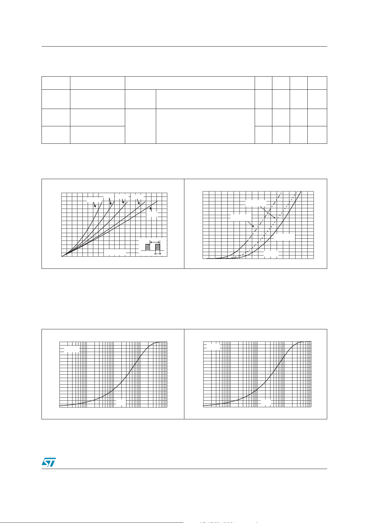
Figure 1. Conduction losses versus average
forward current
P(W)
4.0
3.5
3.0
2.5
2.0
1.5
1.0
0.5
0.0
0.00 0.25 0.50 0.75 1.00 1.25 1.50 1.75 2.00 2.25 2.50
δ = 0.05
δ = 0.1
I (A)
F(AV)
δ = 0.2
δ = 0.5
δ
=tp/T
δ = 1
T
tp
Figure 3. Relative variation of thermal
impedance junction to ambient
versus pulse duration (Epoxy
printed circuit board FR4,
L
Z
th(j-a)/Rth(j-a)
1.0
DO-201AD
0.9
=10mm
L
leads
0.8
0.7
0.6
0.5
0.4
0.3
0.2
0.1
0.0
1.E-01 1.E+00 1.E+01 1.E+02 1.E+03
Leads
= 10mm)
tp(s)
Figure 2. Forward voltage drop versus
forward current
I (A)
FM
50
45
40
35
30
25
20
15
10
5
0
0.0 0.5 1.0 1.5 2.0 2.5 3.0 3.5 4.0 4.5
T=125°C
j
(typical values)
T=125°C
j
(maximum values)
V (V)
FM
T=25°C
j
(maximum values)
Figure 4. Relative variation of thermal
impedance junction to ambient
versus pulse duration (Epoxy
printed circuit board FR4,
S
=1cm2)
CU
Z
th(j-a)/Rth(j-a)
1.0
SMB
0.9
S
=1cm²
Cu
0.8
0.7
0.6
0.5
0.4
0.3
0.2
0.1
0.0
1.E-01 1.E+00 1.E+01 1.E+02 1.E+03
tp(s)
3/9
 Loading...