


ST STTH20LCD06C User Manual
STTH20LCD06C
Turbo2 ultrafast - high voltage rectifier for SMPS
Features
■ ultrafast switching
■ low reverse current
■ low thermal resistance
■ reduces conduction and switching losses
Description
The STTH20LCD06C uses ST Turbo2 technology.
This device is specially suited for switching power
supplies working with interleaved PFCs.
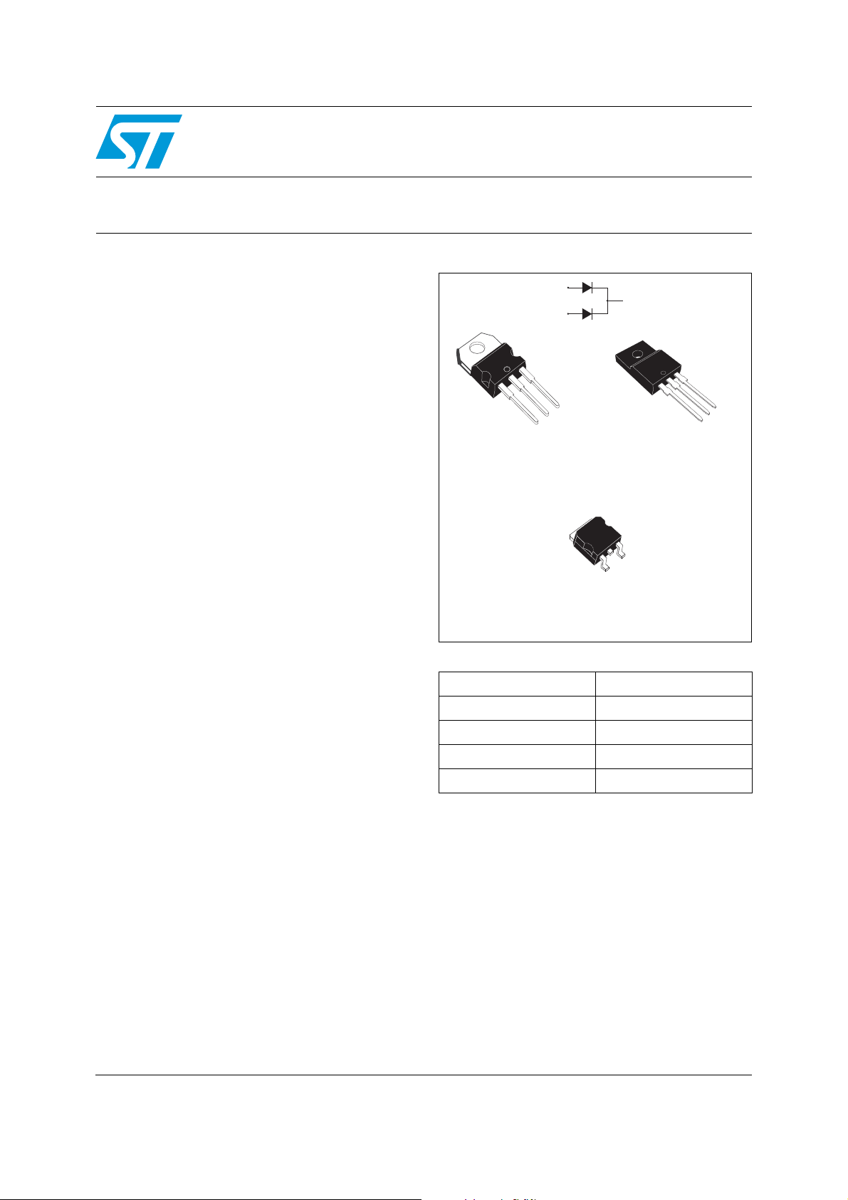
A1
A2
A2
K
A1
TO-220AB
STTH20LCD06CT
STTH20LCD06CFP
K
A1
D2PAK
STTH20LCD06CG-TR
Table 1. Device summary
I
F(AV)
V
RRM
T
j
(typ) 1.25 V
V
F
t
(max) 50 ns
rr
K
TO-220FPAB
A2
2 x 10 A
600 V
175 °C
A1
A2
K
January 2011 Doc ID 15898 Rev 2 1/10
www.st.com
10

Characteristics STTH20LCD06C
1 Characteristics
Table 2. Absolute ratings
(1)
Symbol Parameter Value Unit
V
I
F(RMS)
I
F(AV)
I
T
1. Limiting values per diode at 25 °C, unless otherwise specified
2. condition to avoid thermal runaway for a diode on its own heatsink
Table 3. Thermal resistance
Repetitive peak reverse voltage 600 V
RRM
Forward current rms 30 A
TO-220AB,
2
PA K
D
Average forward
= 105 °C
T
c
current, δ = 0.5
= 60 °C TO-220FPAB
T
c
Surge non repetitive forward current tp = 10 ms sinusoidal 80 A
FSM
Storage temperature range -65 to + 175 °C
stg
Maximum operating junction temperature
T
j
<
Rth(j-a)
1
dPtot
dTj
(2)
Per diode 10 A
Per device 20 A
Per diode 10 A
Per device 20 A
175 °C
Symbol Parameter Value Unit
2
PA K 3 .5
°C/W
R
Table 4. Static electrical characteristics
th(j-c)
Junction to case
TO-220AB, D
TO-220FPAB 5.8
Symbol Parameter Test conditions Min. Typ. Max. Unit
Reverse leakage
(1)
I
R
current
(2)
V
1. Pulse test: tp = 5 ms, δ < 2 %
2. Pulse test: tp = 380 µs, δ < 2 %
Forward voltage drop
F
= 25 °C
T
j
= 150 °C - 10 100
T
j
= 25 °C
T
j
T
= 150 °C - 1.25 1.6
j
= 25 °C
T
j
T
= 150 °C - 1.55 2
j
= V
V
R
I
= 10 A
F
= 20 A
I
F
RRM
--1
--2
- - 2.35
To evaluate the conduction losses use the following equation:
P = 1.2 x I
F(AV)
+ 0.04 x I
F2(RMS)
µA
V
2/10 Doc ID 15898 Rev 2
STTH20LCD06C Characteristics
Table 5. Dynamic electrical characteristics
Symbol Parameter
Test conditions
I
= 0.5 A, Irr = 0.25 A,
F
IR = 1 A, Tj = 25 °C
t
Reverse recovery time
rr
I
V
Reverse recovery current
RM
t
Forward recovery time
fr
Forward recovery voltage
FP
= 1 A, dIF/dt = -50 A/µs,
I
F
= 30 V, Tj = 25 °C
V
R
= 10 A, dIF/dt = -50 A/µs,
I
F
VR = 400 V, Tj = 125 °C
I
= 10 A, dIF/dt = 100 A/µs
F
VFR = 1.1 x V
= 10 A, dIF/dt = 100 A/µs
I
F
= 1.1 x V
V
FR
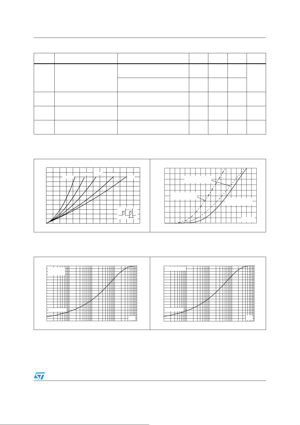
Figure 1. Average forward power dissipation
versus average forward current
(per diode)
P
(W)
F(AV)
24
δ = 0.2
20
16
12
8
4
0
02468101214
δ = 0.05
δ = 0.1
δ = 0.5
δ = tp/T
δ = 1
T
t
p
Min. Typ. Max. Unit
25
35 50
22.8A
, Tj = 25 °C
Fmax
, Tj = 25 °C
Fmax
4V
230 ns
Figure 2. Forward voltage drop versus
forward current (per diode)
IFM(A)
100
80
60
(Typical values)
40
20
0
0.0 0.5 1.0 1.5 2.0 2.5 3.0 3.5 4.0 4.5
(Maximum values)
Tj= 150 °C
Tj= 150 °C
Tj= 25 °C
(Maximum values)
ns
VFM(V)
Figure 3. Relative variation of thermal
impedance junction to case versus
pulse duration (TO-220AB, D
Z
th(j-c)/Rth(j-c)
1.0
TO-220AB
0.9
D2PAK
0.8
0.7
0.6
0.5
0.4
0.3
Single pulse
0.2
0.1
0.0
1.E-04 1.E-03 1.E-02 1.E-01 1.E+00
Figure 4. Relative variation of thermal
impedance junction to case versus
2
PAK)
1.0
0.9
0.8
0.7
0.6
0.5
0.4
0.3
0.2
tp(s)
Doc ID 15898 Rev 2 3/10
0.1
0.0
1.E-03 1.E-02 1.E-01 1.E+00 1.E+01
pulse duration (TO-220FPAB)
Z
th(j-c)/Rth(j-c)
TO-220FPAB
Single pulse
tp(s)