


Features
STTH20L03C
High frequency secondary rectifier
Datasheet − production data
■ Ultrafast, soft and noise-free recovery
■ Low forward voltage drop
Description
Dual center tap fast recovery epitaxial diodes
suited for switch mode power supply and high
frequency DC/DC converters.
Packaged in TO-220AB or D
especially intended for secondary rectification
inside SMPS with high space and power-density.
2
PAK, this device is
A1
A2
A2
K
A1
TO-220AB
STTH20L03CT
Table 1. Device summary
Symbol Value
I
F(AV)
V
RRM
T
j
V
(max) 0.95 V
F
(typ) 26 ns
t
rr
K
K
A2
A1
D2PAK
STTH20L03CG
2 x 10 A
300 V
-40 to +175 °C
June 2012 Doc ID 023115 Rev 1 1/9
This is information on a product in full production.
www.st.com
9

Characteristics STTH20L03C
1 Characteristics
Table 2. Absolute ratings (limiting values, per diode, at 25 °C, unless otherwise specified)
Symbol Parameter Value Unit
V
I
F(RMS)
I
F(AV)
I
T
Table 3. Thermal resistance
Repetitive peak reverse voltage 300 V
RRM
Forward rms current 30 A
T
= 155 °C
Average forward current, δ = 0.5
Surge non repetitive forward current tp = 10 ms sinusoidal 150 A
FSM
Storage temperature range -65 to + 175 °C
stg
Operating junction temperature range -40 to +175 °C
T
j
c
= 150 °C
T
c
Per diode
Per device
10
20
Symbol Parameter Value (max) Unit
Per diode 1.5
R
R
Junction to case
th(j-c)
Coupling 0.5
th(c)
°C/WTo ta l 1 .0
When diodes 1 and 2 are used simultaneously:
Tj
(diode 1)
Table 4. Static electrical characteristics (per diode)
= P
(diode 1)
x R
(Per diode) + P
th(j-c)
(diode 2)
x Rth(c)
A
Symbol Parameter Test conditions Min. Typ. Max. Unit
(1)
I
V
1. Pulse test: tp = 5 ms, δ < 2%
2. Pulse test: t
Reverse leakage current
R
(2)
Forward voltage drop
F
= 380 µs, δ < 2%
p
= 25 °C
j
= 125 °C 10 100
T
j
T
= 25 °C
j
Tj = 125 °C 0.8 0.95
= V
V
R
= 10 A
I
F
RRM
0.95 1.2
10
T
To evaluate the conduction losses use the following equation:
P = 0.8 x I
+ 0.015 I
F(AV)
F2(RMS))
µA
V
2/9 Doc ID 023115 Rev 1
STTH20L03C Characteristics
Table 5. Dynamic electrical characteristics (per diode)
Symbol Parameter Test conditions Min. Typ. Max. Unit
T
= 25 °C
j
t
Reverse recovery time
rr
= 125 °C
T
j
I
Reverse recovery current
S
Q
RM
factor
RR
t
fr
V
FP
Softness factor 0.3
Reverse recovery charges
Forward recovery time
Forward recovery voltage 2.5 3.5 V
Tj = 125 °C
T
= 125 °C IF = 10 A, VR = 200 V
j
= 25 °C
T
j
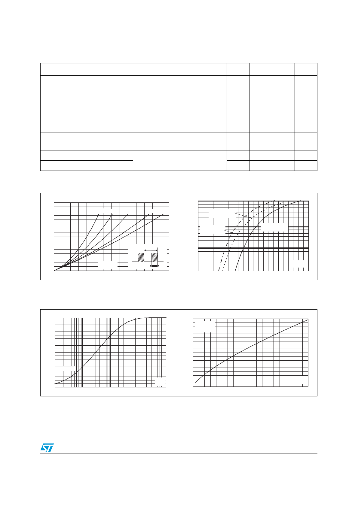
Figure 1. Conduction losses versus average
forward current (per diode)
P
(W)
F(AV)
16
14
12
10
8
6
4
2
0
02468101214
δ = 0.05 δ = 0.1
I
F(AV)
δ = 0.2
(A)
=tp/T
δ
δ = 0.5
T
Figure 3. Relative variation of thermal
impedance junction to case versus
pulse duration
Z
th(j-c)/Rth(j-c)
1.0
0.9
0.8
0.7
0.6
0.5
0.4
0.3
Single pulse
0.2
0.1
0.0
1.E-04 1.E-03 1.E-02 1.E-01 1.E+00
IF = 1 A, VR= 30 V
dIF/dt = -100 A/µs
IF = 10 A, VR = 200 V
dIF/dt = -200 A/µs
IF = 10 A, VR = 200 V
/dt = -200 A/µs
dI
F
/dt = -200 A/µs
dI
F
IF = 10 A, VFR = 1.05 V
dIF/dt = 100 A/µs
Figure 2. Forward voltage drop versus
100.0
δ = 1.0
10.0
1.0
tp
0.1
Figure 4. Peak reverse recovery current
IRM(A)
18
16
14
12
10
8
6
4
tp(s)
2
0
0 50 100 150 200 250 300 350 400 450 500
26 35
55 72
912A
250 375 nC
200 ns
forward current (per diode)
IFM(A)
Tj=125 °C
(Maximum values)
Tj=125 °C
(Typical values)
0.0 0.2 0.4 0.6 0.8 1.0 1.2 1.4 1.6 1.8 2.0 2.2
versus dI
/dt (typical values, per
F
Tj=25 °C
(Maximum values)
VFM(V)
diode)
IF=I
F(AV)
VR=200 V
T
=125 °C
j
dIF/dt(A/µs)
ns
Doc ID 023115 Rev 1 3/9
 Loading...