

ST STTH200L04TV1 User Manual
Features
■ Ultrafast switching
■ Low reverse current
■ Low thermal resistance
■ Reduces switching and conduction losses
■ Package insulation voltage: 2500 V
RMS
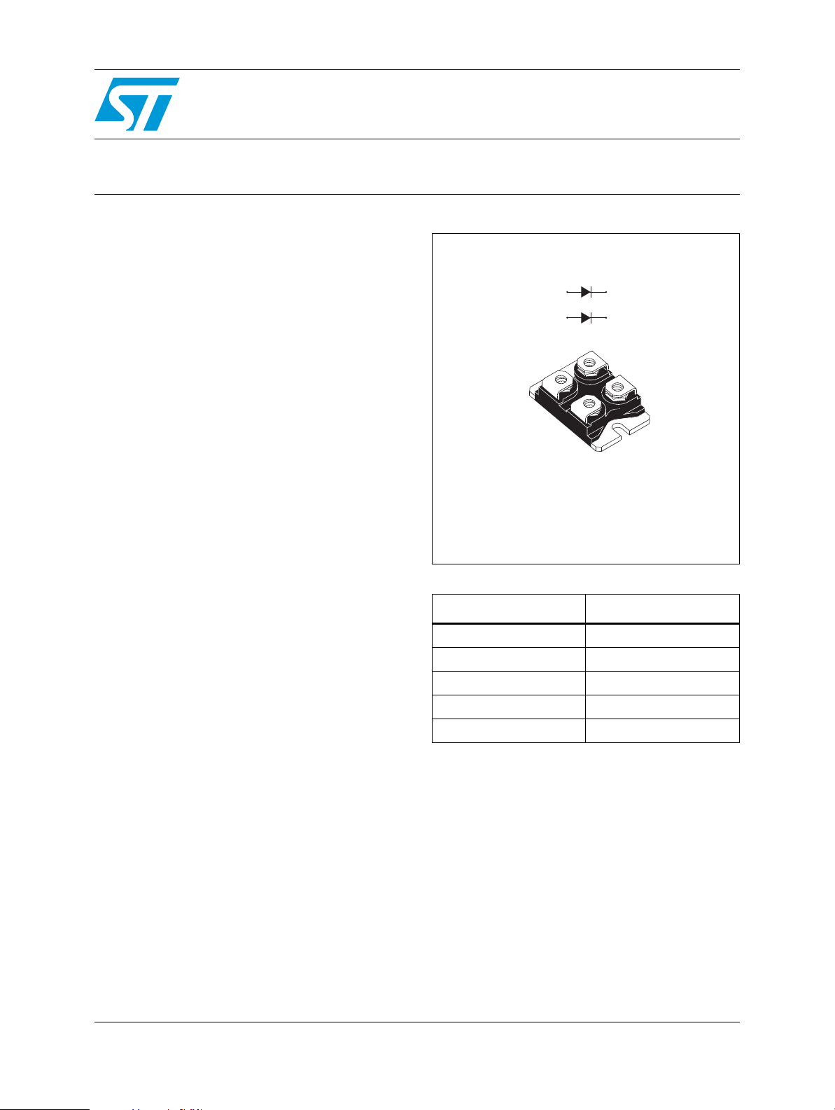
STTH200L04TV1
Ultrafast high voltage rectifier
A1 K1
A2 K2
K1
A1
Description
The STTH200L04TV1 uses ST 400 V technology
and is specially suited for use in switching power
supplies, welding equipment, and industrial
applications, as an output rectification diode.
K2
A2
ISOTOP
STTH200L04TV1
Table 1. Device summary
Symbol Value
I
F(AV)
V
RRM
(max) 150 °C
T
j
(typ) 0.83 V
V
F
t
(max) 50 ns
rr
up to 2 x 120 A
400 V
September 2011 Doc ID 12827 Rev 2 1/8
www.st.com
8
Characteristics STTH200L04TV1
1 Characteristics
Table 2. Absolute ratings (limiting values, per diode)
Symbol Parameter Value Unit
V
I
F(RMS)
I
F(AV)
I
T
Table 3. Thermal resistance
Repetitive peak reverse voltage 400 V
RRM
Forward rms current 200 A
T
= 90 °C δ = 0.5 Per diode 100
Average forward current
Surge non repetitive forward
FSM
current
Storage temperature range -55 to + 150 °C
stg
Maximum operating junction temperature 150 °C
T
j
c
= 73 °C δ = 0.5 Per diode 120
T
c
= 10 ms sinusoidal 900 A
t
p
Symbol Parameter
R
R
Junction to case
th(j-c)
Coupling 0.10
th(c)
When diodes 1 and 2 are used simultaneously:
Δ Tj(diode 1) = P(diode 1) x R
Table 4. Static electrical characteristics (per diode)
(Per diode) + P(diode 2) x R
th(j-c)
Value
(max).
Per diode 0.50
th(c)
A
Unit
°C/WTo tal 0 .30
Symbol Parameter Test conditions Min. Typ. Max. Unit
= 25 °C
T
Reverse leakage
(1)
I
R
current
(2)
V
1. Pulse test: tp = 5 ms, δ < 2%
2. Pulse test: tp = 380 µs, δ < 2%
Forward voltage drop
F
j
= 125 °C 100 1000
T
j
T
= 25 °C
j
= 150 °C 0.83 1.0
T
j
VR = V
= 100 A
I
F
To evaluate the conduction losses use the following equation:
P = 0.8 x I
2/8 Doc ID 12827 Rev 2
+ 0.002 I
F(AV)
F2(RMS)
RRM
100
µA
1.2
V
STTH200L04TV1 Characteristics
Table 5. Dynamic characteristics (per diode)
Symbol Parameter Test conditions Min. Typ. Max. Unit
I
= 1 A dIF/dt = 50 A/µs
Reverse recovery
S
t
rr
I
RM
factor
t
fr
V
FP
time
Reverse recovery
current
Softness factor Tj = 125 °C
Forward recovery
time
Forward recovery
voltage
= 25 °C
T
j
= 125 °C
T
j
T
= 25 °C
j
= 25 °C
T
j
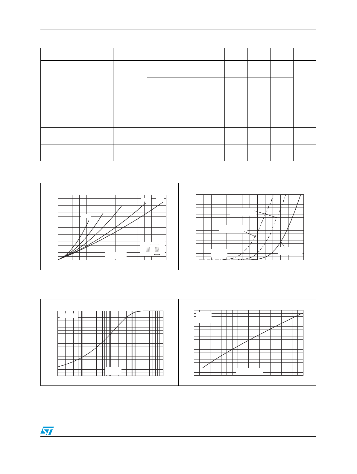
Figure 1. Conduction losses versus
average forward current (per diode)
P(W )
180
160
140
120
100
80
60
40
20
0
0 10 20 30 40 50 60 70 80 90 100 110 120 130 140 150
δ=0.05
δ=0.1
I
F(AV)
δ=0.2
(A)
δ=0.5
δ
=tp/T
F
= 30 V
V
R
= 1 A dIF/dt = 200 A/µs
I
F
= 30 V
V
R
I
= 100 A VR = 200 V
F
dIF/dt = 100 A/µs
= 100 A VR = 200 V
I
F
/dt = 100 A/µs
dI
F
= 100 A dIF/dt = 200 A/µs
I
F
= 1.1 x V
V
FR
I
= 100 A dIF/dt = 200 A/µs
F
VFR = 1.1 x V
Fmax
Fmax
Figure 2. Forward voltage drop versus
I
(A)
I
FM
δ=1
T
tp
200
180
160
140
120
100
80
60
40
20
0
0.0 0.2 0.4 0.6 0.8 1.0 1.2 1.4
forward current (per diode)
Tj=150°C
Tj=150°C
(Maximum values)
(Maximum values)
Tj=150°C
Tj=150°C
(Typical values)
(Typical values)
VFM(V)
75 100
45 60
18 A
0.4
800 ns
2.6 V
Tj=25°C
(Maximum values)
ns
Figure 3. Relative variation of thermal
impedance junction to case versus
pulse duration
/R
Z
th (j-c)
1.0
0.9
0.8
0.7
0.6
0.5
0.4
0.3
0.2
0.1
0.0
1.E-03 1.E-02 1.E-01 1.E+00 1.E+01
th(j-c)
Single pulse
tP(s)
Figure 4. Peak reverse recovery current
versus dI
/dt
F
(typical values, per diode)
I
(A)
RM
50
IF=I
F(AV)
45
VR=200V
T
=125°C
j
40
35
30
25
20
15
10
5
0
0 50 100 150 200 250 300 350 400 450 500
Doc ID 12827 Rev 2 3/8
dIF/dt(A/µs)
 Loading...