

ST STTH20003TV User Manual
Mian product characteristics
STTH20003TV
Ultrafast high voltage rectifier
I
F(AV)
V
RRM
T
(max) 150° C
j
(typ) 0.95 V
V
F
(max) 90 ns
t
rr
Features and benefits
■ Combines highest recovery and reverse
voltage performance
■ Ultrafast, soft and noise-free recovery
■ Package insulation voltage 2500 V
■ low inductance and low capacitance allow
up to 2 x 100 A
300 V
rms
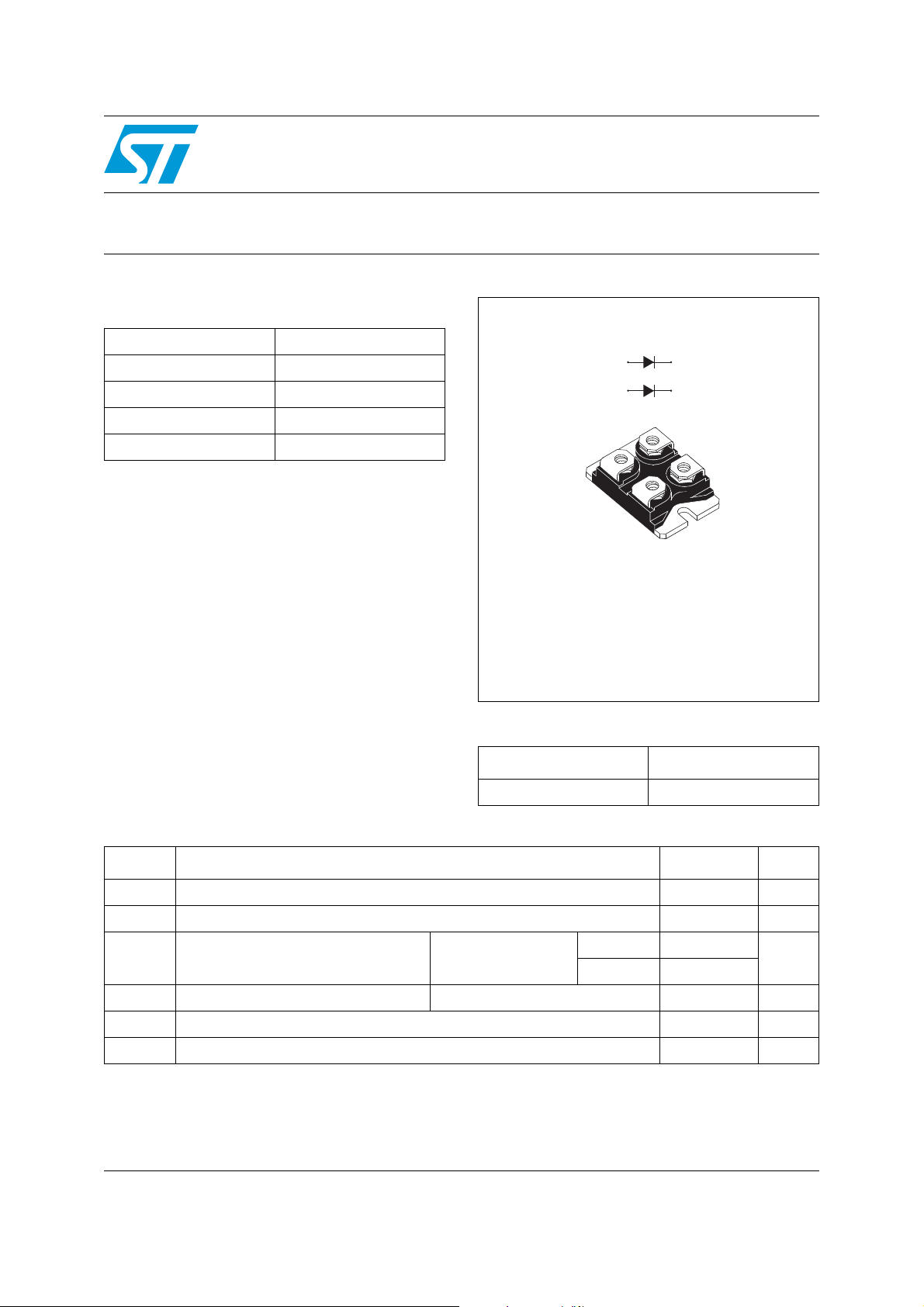
A1 K1
A2 K2
K1
A1
K2
A2
ISOTOP
STTH20003TV
simpler layout
Description
Dual rectifiers suited for Switch Mode Power
Supply and high frequency DC to DC converters.
Packaged in ISOTOP™, this device is intended
for use in low voltage, high frequency inverters,
free wheeling operation, welding equipment and
telecom power supplies.
Table 1. Absolute ratings (limiting values, per diode, Tc = 25° C unless otherwise stated)
Order codes
Part number Marking
STTH20003TV STTH20003TV
Symbol Parameter Value Unit
V
RRM
I
F(RMS)
I
F(AV)
I
FSM
T
TM: ISOTOP is a registered trademark of STMicroelectronics
September 2006 Rev 2 1/7
Repetitive peak reverse voltage 300 V
RMS forward current 180 A
Average forward current Tc = 85° C δ = 0.5
Surge non repetitive forward current tp = 10 ms sinusoidal 100 A
Storage temperature range -55 to + 150 ° C
stg
Maximum operating junction temperature 150 ° C
T
j
Per diode 100
Per device 200
A
www.st.com
7

Characteristics STTH20003TV
1 Characteristics
Table 2. Thermal resistance
Symbol Parameter Value (max). Unit
R
R
Junction to case
th(j-c)
Coupling 0.1
th(c)
°C/WTo ta l 0 .3 5
When diodes 1 and 2 are used simultaneously:
Per diode 0.55
∆ Tj(diode 1) = P(diode 1) x R
Table 3. Static electrical characteristics (per diode)
Symbol Parameter Test conditions Min. Typ Max. Unit
Reverse leakage
(1)
I
R
current
(2)
V
1. Pulse test: tp = 5 ms, δ < 2%
2. Pulse test: tp = 380 µs, δ < 2%
Forward voltage drop
F
(Per diode) + P(diode 2) x R
th(j-c)
= 25° C
T
j
T
= 125° C 0.2 2 mA
j
T
= 25° C
j
Tj = 150° C 0.8 0.95
= 300 V
V
R
= 100 A
I
F
th(c)
200 µA
1.20
V
To evaluate the conduction losses use the following equation:
P = 0.75 x I
Table 4. Dynamic characteristics (per diode)
Symbol Parameter Test conditions Min Typ Max Unit
+ 0.0020 I
F(AV)
F2(RMS)
S
t
rr
I
RM
factor
t
fr
V
FP
Reverse recovery
time
Reverse recovery
current
Softness factor Tj = 125° C
Forward recovery
time
Forward recovery
voltage
= 25° C
T
j
T
= 125° C
j
= 25° C
T
j
T
= 25° C
j
2/7
= 0.5 A Irr = 0.25 A IR = 1 A 55
I
F
I
= 1 A dIF/dt = -50 A/µs
F
= 30 V
V
R
= 100 A VR = 200 V
I
F
dIF/dt = -200 A/µs
I
= 100 A VR = 200 V
F
dI
/dt = -200 A/µs
F
= 100 A dIF/dt = 200 A/µs
I
F
= 1.1 x V
V
FR
= 100 A dIF/dt = 200 A/µs
I
F
VFR = 1.1 x V
Fmax
Fmax
ns
90
18 A
0.3
1400 ns
5V
STTH20003TV Characteristics
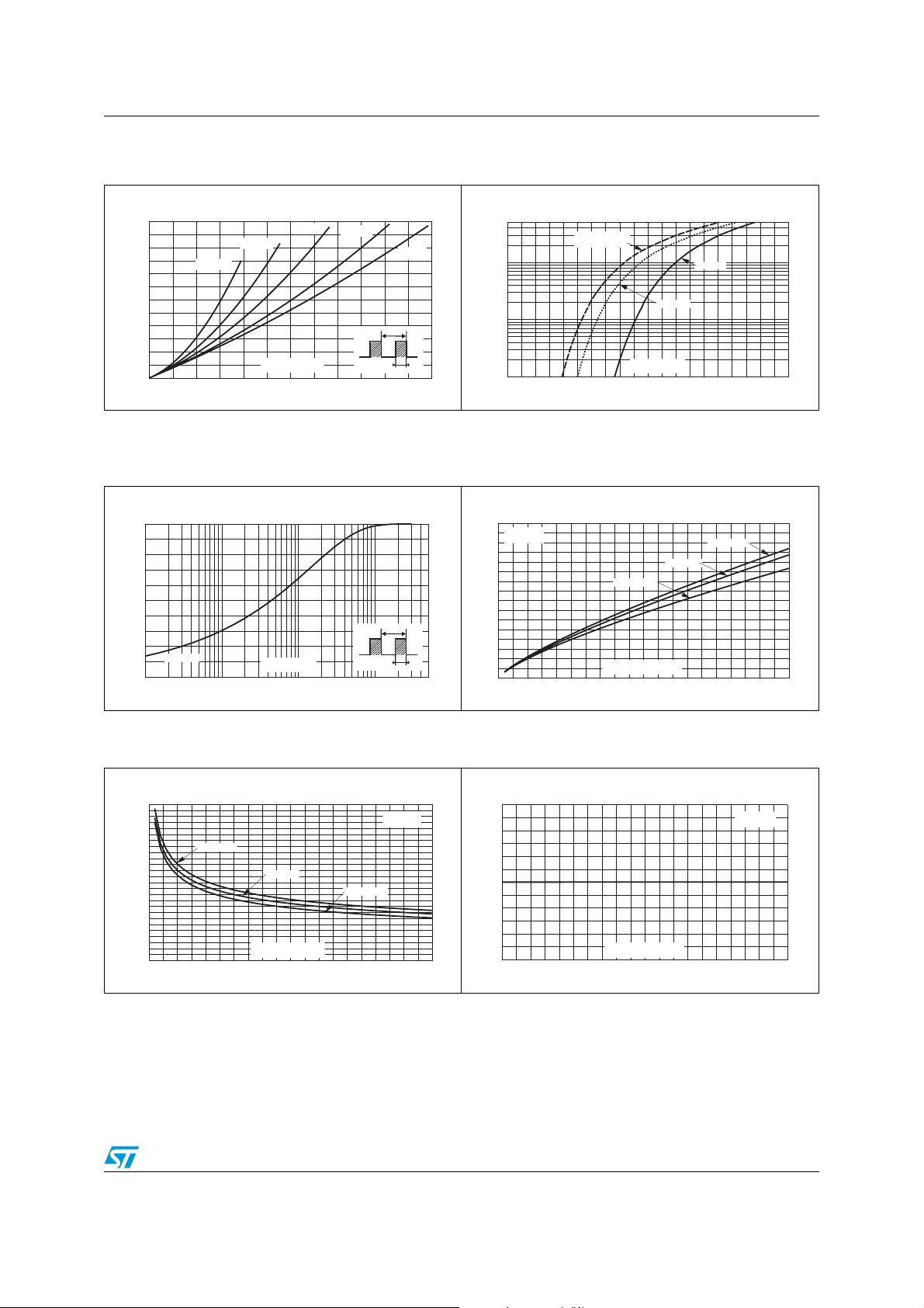
Figure 1. Conduction losses versus
average forward current (per diode)
P1(W)
120
100
80
δ = 0.1
δ = 0.05
δ = 0.2
δ = 0.5
60
40
20
0
0 20 40 60 80 100 120
I (av) (A)
F
δ
=t /T
T
p
Figure 3. Relative variation of thermal
impedance junction to case versus
pulse duration
Z/R
th(j-c) th(j-c)
1.0
0.8
0.6
0.4
0.2
Single pulse
0.0
1E-3 1E-2 1E-1 1E+0 5E+0
t (s)
p
δ
=t /T
T
p
δ = 1
Figure 2. Forward voltage drop versus
forward current (per diode)
I (A)
FM
500
100
Tj=125°C
(Typical values)
Tj=25°C
Tj=125°C
10
t
p
1
0.0 0.2 0.4 0.6 0.8 1.0 1.2 1.4 1.6 1.8 2.0
V (V)
FM
Figure 4. Peak reverse recovery current
versus dI
/dt (90% confidence, per
F
diode)
I (A)
RM
40
V =200V
R
T =125°C
j
35
30
I =0.5xI (av)
25
FF
20
15
10
t
p
5
0
0 50 100 150 200 250 300 350 400 450 500
dI /dt(A/µs)
F
IF=I (av)
F
I =2xI (av)
FF
Figure 5. Reverse recovery time versus
dI
/dt (90% confidence, per diode)
F
t (ns)
rr
260
240
220
200
180
160
140
120
100
80
60
40
20
0
0 50 100 150 200 250 300 350 400 450 500
I =2xI (av)
FF
I=I(av)
FF
dI /dt(A/µs)
F
I =0.5xI (av)
FF
V =200V
R
T =125°C
j
Figure 6. Softness factor (t
dI
/dt (typical values, per diode)
F
S factor
0.6
0.5
) versus
b/ta
V =200V
R
T =125°C
j
0.4
0.3
0.2
0.1
dI /dt(A/µs)
0.0
0 50 100 150 200 250 300 350 400 450 500
F
3/7
 Loading...