

Automotive high efficiency ultrafast diode
Features
■ Very low conduction losses
■ Negligible switching losses
■ Low forward and reverse recovery times
■ High junction temperature
■ ECOPACK
■ AEC-Q101 qualified
Description
The STTH102-Y, which is using ST’s new 200 V
planar technology, is specially suited for switching
mode base drive and transistor circuits. The
device is also intended for use as a free wheeling
diode in power supplies and other power
switching applications for automotive.
®
2 compliant component
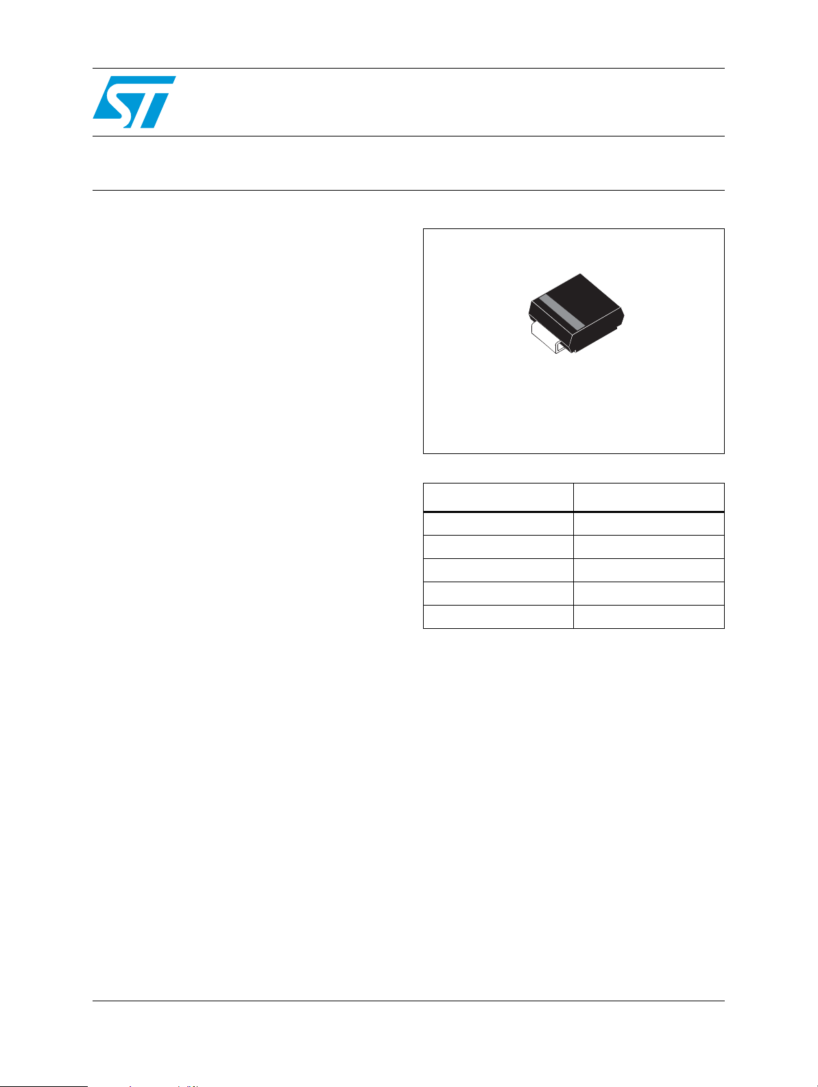
STTH102-Y
K
SMA
(JEDEC DO-214AC)
STTH102AY
Table 1. Device summary
Symbol Value
I
F(AV)
V
RRM
T
(max) 175 °C
j
(max) 0.78 V
V
F
(max) 20 ns
t
rr
A
1 A
200 V
November 2011 Doc ID 17982 Rev 1 1/7
www.st.com
7

Characteristics STTH102-Y
1 Characteristics
Table 2. Absolute rating (limiting values)
Symbol Parameter Value Unit
V
I
F(AV)
I
T
Repetitive peak reverse voltage 200 V
RRM
Average forward current TL = 148 °C δ = 0.5 1 A
Surge non repetitive forward current tp = 10 ms sinusoidal 40 A
FSM
Storage temperature range -65 to + 175 °C
stg
Operating junction temperature range -40 to +175 °C
T
j
dV/dt Critical rate of rise of reverse voltage 10000 V/µs
Table 3. Thermal resistance
Symbol Parameter Value Unit
R
Table 4. Static Electrical Characteristics
Junction to lead 30 °C/W
th(j-l)
Symbol Parameter Tests conditions Min. Typ. Max. Unit
IR
(1)
Reverse leakage current
= 25 °C
j
= 125 °C 1 25
T
j
= V
V
R
RRM
1
T
IF = 700 mA 0.90
T
= 25 °C
(2)
V
1. Pulse test: tp = 5 ms, δ < 2%
2. Pulse test: t
Forward voltage drop
F
= 380 µs, δ < 2%
p
j
= 125 °C IF = 1 A 0.68 0.78
T
j
= 1 A 0.97
F
µA
VI
To evaluate the conduction losses use the following equation: P = 0.65 x I
Table 5. Dynamic electrical characteristics
F(AV)
+ 0.130 I
F2(RMS)
Symbol Parameter Tests conditions Min. Typ. Max. Unit
= 0.5 A Irr = 0.25 A
I
t
Reverse recovery time Tj = 25 °C
rr
t
Forward recovery time Tj = 25 °C
fr
V
Forward recovery
FP
voltage
T
= 25 °C IF = 1 A dIF/dt = 50 A/ms 1.8 V
j
F
= 1 A
I
R
= 1 A dIF/dt = 50 A/ms
I
F
= 1.1 x VFmax
V
FR
12 20 ns
50 ns
2/7 Doc ID 17982 Rev 1
STTH102-Y Characteristics
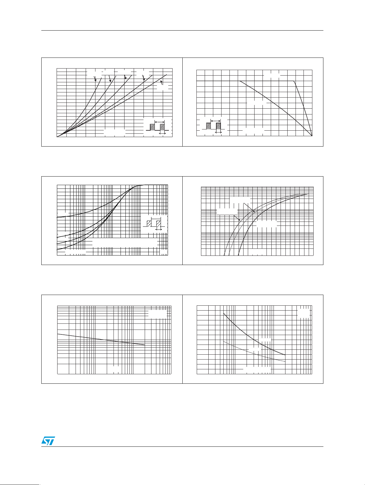
Figure 1. Average forward power dissipation
versus average forward current
P (W)
F(AV)
1.0
0.9
0.8
0.7
0.6
0.5
0.4
0.3
0.2
0.1
0.0
0.0 0.2 0.4 0.6 0.8 1.0 1.2
δ = 0.05
δ = 0.1
I (A)
F(AV)
δ = 0.2
δ = 0.5
δ
=tp/T
δ = 1
T
tp
Figure 3. Relative variation of thermal
impedance junction to ambient
versus pulse duration
Z/R
th(j-a) th(j-a)
1.0
0.9
0.8
0.7
0.6
0.5
0.4
0.3
0.2
0.1
0.0
δ = 0.5
δ = 0.2
δ = 0.1
Single pulse
epoxy printed circuit board,
e = 35 µm, recommended pad layout
(Cu)
δ
=t /T
T
t
p
p
t (s)
p
1.E-01 1.E+00 1.E+01 1.E+02 1.E+03
Figure 5. Junction capacitance versus
reverse voltage applied
(typical values)
C(pF)
100
10
V (V)
1
1 10 100 1000
R
F=1MHz
V =30mV
OSC RMS
T=25°C
j
Figure 2. Average forward current versus
ambient temperature (δ = 0.5)
I (A)
F(AV)
1.2
1.0
0.8
0.6
0.4
0.2
0.0
0 25 50 75 100 125 150 175
δ
=tp/T
T
tp
T (°C)
R =120°C/W
th(j-a)
amb
R=R
th(j-a) th(j-I)
Figure 4. Forward voltage drop versus
forward current
I (A)
FM
100.0
T=125°C
j
(maximum values)
10.0
1.0
0.1
0.0 0.2 0.4 0.6 0.8 1.0 1.2 1.4 1.6 1.8 2.0 2.2 2.4
T=125°C
j
(typical values)
(maximum values)
V (V)
FM
T=25°C
j
Figure 6. Reverse recovery time versus dIF/dt
(90% confidence)
t (ns)
rr
70
60
50
40
30
20
10
0
1 10 100 1000
T=125°C
j
T=25°C
j
dI /dt(A/µs)
F
I =1A
F
V =100V
R
T=125°C
j
Doc ID 17982 Rev 1 3/7
 Loading...