


■ SUPPLY VOLTAGE RANGE: 4V TO 5.5V
■ TYPICAL PEAK O UTPUT CURRENT:
(SOURCE-SINK: 1.5A)
■ OPERATING FREQUENCY: 20 TO 500 KHz
■ INHIBIT BLANKING TIME: 700 ns
■ AUTOMATIC TURN OFF FOR DUTY-CYCLE
LESS THAN 14%
■ POSSIBILITY TO OPERATE IN
DISCONTINUOUS MODE
STSR30
SYNCHRONOUS RECTIFIER
SMART DRIVER FO R FLYBACK
SO-8
DESCRIPTION
STSR30 Smart Driver IC provides a high c urrent
outputs to properly drive secondary Power
Mosfets used as Synchronous Rectifier in low
output voltage, high efficiency Flyback
Converters. From a synchronizing clock inp ut,
withdrawn on the secondary side of the isolation
transformer, the IC generates a driving s ignal with
set dead times with respect to t he primary side
PWM signal.
The IC operation prevents sec ondary side
shoot-through conditions at turn-on of the primary
BLOCK DIAGRAM
switch providing anticipation in turn-off the output.
This smart function is implemented by a fast
cycle-after-cycle logic control mechanism, based
on a high freq uenc y oscillator synchronized by the
clock signal. This anticipation is externally set
through external component. A special Inhibit
function, detec ting the voltage across the
Synchronous FET, allows to shut-off the drive
output during discontinuous mode condition. A
Disable pin allows turning off the device during
no-load condition reducing overall current
consumption.
1/10January 2004
STSR30
ABSOLUTE MAXIMUM RATINGS (Note 1)
Symbol Parameter Value Unit
V
OUT
DISABLE
INHIBIT
CK Clock Input Voltage Range (*) -0.3 to V
ESD Human Body Model ±2KV
P
TOT
T
STG
T
Absolute Maximum Ratings are those values beyond which damage to the device may occur. Functional operation under these condition is
not implied.
(*) A higher positive voltage level can be applied to the pin with a resistor which limits the current flowing into the pin to 10mA maximum
THERMAL DATA
Symbol Parameter SO-8 Unit
R
thj-case
R
thj-amb
(*) This value is referred to one layer pcb board with minimum copper connections for the leads. A minimum value of 120 °C/W can be
obtained improving thermal conductivity of the board
DC Input Voltage to SGLGND
CC
Max Gate Drive Output Voltage -0.3 to V
GATE
Max DISABLE Voltage -0.3 to V
Max INHIBIT Voltage (*) -0.6 to V
-0.3 to 6 V
CC
CC
CC
CC
Continuous Power Dissipation at TA=105°C SO-8 (No heatsink) 275 mW
Storage Temperature Range
Operating Junction Temperature Range -40 to +125 °C
OP
Thermal Resistance Junction-case
Thermal Resistance Junction-ambient (*)
-40 to +150 °C
40 °C/W
160 (*) °C/W
V
V
V
V
ORDERING CODES
TYPE SO-8 SO-8 (T&R)
STSR30 STSR30D STSR30D-TR
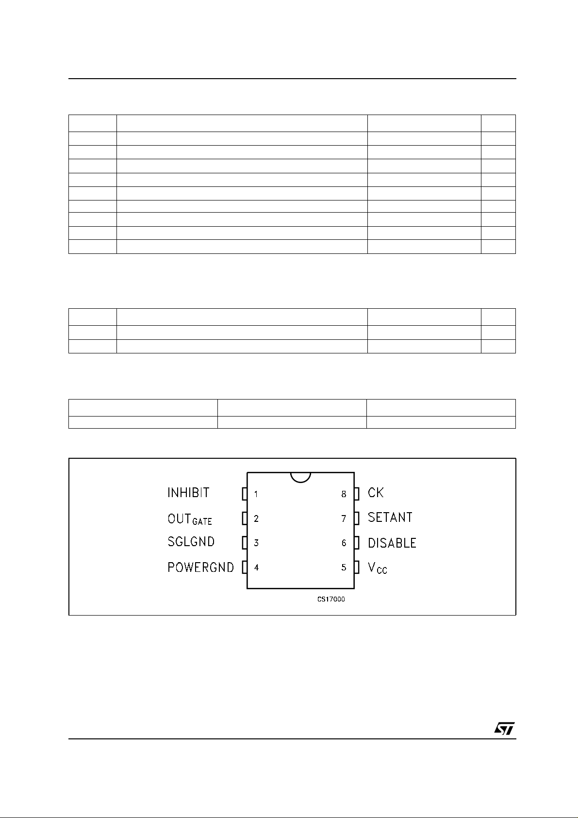
CONNECTION DIAGRAM (top view)
2/10
PIN DESCRIPTION
Pin N° Symbol Name and Function
1 INHIBIT This input enables OUT
threshold voltage (V
INHIBIT<VH
minimum conduction time (t
possible to turn off the synchronous MOSFET when the current through it tends to
reverse, allowing discontinuous conduction mode and providing protection to the
converter from eventual sinking current from the load.
A blanking time of 700ns allows operation when some voltage ringing is present
during turn-off of primary switch.
Absolute maximum voltage rating of the pin can be exceeded limiting the current
flowing into the pin to 10mA max.
2OUT
GATE
Gate Drive signal for Synchronous MOSFET. Anticipation [t
OUT
is provided when the clock input goes to low level.
GATE
3 SGLGND Reference for all the control logic signals. This pin is completely separated from
the PWRGND to prevent eventual disturbances to affect the control logic.
4 PWRGND Reference for power signals, this pin carries the full peak currents for the output.
5V
CC
The supply voltage range from 4.5V to 5.5V allows applications with logic gate
threshold mosfets. UVLO feature guarantees proper start-up while it avoids
undesirable driving during eventual dropping of the supply voltage.
6 DISABLE This pin allows turning off the device completely when kept to low level. In this
condition the IC power consumption is strongly reduced. When this pin goes to
high value, OUT
GATE
7 SETANT The voltage on this pin sets the anticipation in turning off the OUTGATE. It is
possible to choose among three different anticipation times by discrete
partitioning of the supply voltage [ANT].
8 CK This input provides synchronization for IC’s operations, being the transitions
between the two output conditions based on a positive threshold, equal for the
two slopes. A smart internal control logic mechanism using a 15MHz internal
oscillator generates proper anticipation timing at the turn-off of each output. This
feature allows safe turn-off of Synchronous Rectifiers avoiding any eventual
shoot-through situation on secondary side at both transitions. Clock revelation
mechanism makes the operation of STSR30 particularly suitable for flyback
adaptors application allowing correct operation during discontinuous mode.
Absolute maximum positive voltage rating of the pin can be exceeded limiting the
current flowing into the pin to 10mA max.
to work when its voltage is lower than the negative
GATE
). If V
INHIBIT>VH
ON(GATE)
). In typical flyback converter application, it is
turns to switching again according to the CK signal.
the OUT
will be high for a
GATE
] in turning off
ANT
STSR30
3/10

STSR30
ELECTRICAL CHARACTERISTICS (VCC= 5V, CK = 100kHz, duty-cycle = 50%, V
= -40 to 125°C, C1=C2= 100nF ceramic, unless otherwise specified.)
T
J
INHIBIT
= -200mV,
Symbol Parameter Test Conditions Min. Typ. Max. Unit
SUPPLY INPUT AND UNDER VOLTAGE LOCK OUT
V
Start Threshold 3.7 4 V
CC
Turn OFF Threshold After Start 3.3 3.6
I
Unloaded Supply Current OUT
CC
= no load 3.2 4.5 mA
GATE
DISABLE = 0V 15 50 µA
GATE DRIVER OUTPUT
OUT
I
R
DS(ON)
OUT
Output Low Voltage I
GATE
Output High Voltage I
OUTGATE
OUTGATE
= -200mA 0.20 0.45 V
= 200mA 4.30 4.65
Output Source Peak Current TJ=25°C 1.5 A
Output Sink Peak Current T
=25°C 1.5
J
Output Series Source Resistance 1.75 3.5 Ω
Output Series Sink Resistance 1 2.25
t
Rise Time C
R
Fall Time C
t
F
Clock Propagation Delay to Turn ON
t
P
of OUT
GATE
= 5nF (Note 1) 40 ns
LOAD
= 5nF (Note 1) 40 ns
LOAD
No Load (Fig. 4) 25 ns
TURN-OFF ANTICIPATION TIME
t
ANT
I
SETANT
OUT
(Fig. 1)
Turn-off Anticipation Time
GATE
V
= 0 to 1/3VCC; no load 150 ns
ANT
=1/3VCCto 2/3VCC;noload 225
V
ANT
=2/3VCCto VCC;noload 300
V
ANT
Leakage Current (Note 2) -0.1 0.1 µA
DISABLE
V
V
V
INHIBIT (OUT
V
t
Positive Threshold Voltage V
DP
Negative Threshold Voltage V
DN
Hysteresis Voltage 0.2 V
HY
Input Current -0.1 0.1 µA
I
I
ENABLE)
GATE
Threshold Voltage TJ=25°C -30 -25 mV
H
Leakage Current V
I
H
Blanking Time V
BL
DISABLE>VDP
DISABLE<VDN
INHIBIT
V
INHIBIT
INHIBIT
:ON 1.7 2.4 V
:OFF 0.8 1.5 V
= +200mV -100 nA
= -200mV 1.5 µA
= +200mV 700 ns
SYNCHRONIZATION INPUT
V
Rise Threshold Voltage 1 1.2 V
CK
Fall Threshold Voltage 0.6 0.8
D
Duty Cycle Shut Down 12 14 %
OFF
Duty Cycle Turn ON after Shut Down 19 20
Note1:tRis measured between 10% and 90% of the final voltage; tFis measured between 90%and 10% onthe initial voltage
Note2: Parameter guaranteed by design
4/10

Figure1 : T IMING DIAGRAM
Figure2 : STSR30 IN FLYBACK CONVERTER SECONDARY SIDE
STSR30
Feedback
Loop
TRANSFORMER
Cout
MosfetN
4
PWRGND
C1
100nF
PWM
+5V
R3 D3
R5
2
OUTGate
Ck
INHIBIT
+5V
STSR30
8
1
D1
D2
option
NOTES
1) Ceramic Capacitors C1 and C2 must be placed very close to the IC;
2)R1andR2settheanticipationtimebypartitioningtheV
3) R3 is a pull-up resistor;
CC
voltage;
4) R5 limits the current flowing through diode D2 when Freewheeling drain voltage is high;
5) D1 could be necessary to protect INHIBIT pin from negative voltages.
6) D2 could be necessary to protect INHIBIT pin from voltages higher than V
7) SGLGND layout trace must not include OUTGATE current paths.
CC
5
Vcc
SGLGND
SETANT
DISABLE
6
VoVi
C2
100nF
3
7
Low = OFF
High = ON
+5V
R1
R2
5/10

STSR30
Figure3 : ST SR 30 SYNCHRONIZATION TECHNIQUE
The synchronization is based on the revelation of the low level of the drain voltage of the synchronous rectifier. To avoid false triggering of
the device during discontinuous mode, it is important that the lowest level of the ringing must be higher than the Ck threshold. Diode D3 and
resistor R3 keep the Ck signal to high level even during the ringing. OUTGate is the complementary signal of the Ck with proper dead time
setting to avoid cross-conduction.
Figure4 : INHIBIT OPERATION OF O UT
IN DISCONTINUOUS CONDUCTION MODE
GATE
6/10

STSR30
Figure5 : INHI BIT Thres hold Voltage vs
Temperature
Figure6 : I
vs CK Frequenc y
CC
Figure8 : R
DS(ON)
vs Temperature
Figure9 : Minimum T
ON(GATE)
Figure7 : Ri s e and Fall Time vs Load Capacitor
Figure10 : OUT
Turn-off Jitter with
GATE
Minimum Anticipation Time
7/10

STSR30
SO-8 MECHANICAL DATA
DIM.
A 1.35 1.75 0.053 0.069
A1 0.10 0.25 0.04 0.010
A2 1.10 1.65 0.043 0.065
B 0.33 0.51 0.013 0.020
C 0.19 0.25 0.007 0.010
D 4.80 5.00 0.189 0.197
E 3.80 4.00 0.150 0.157
e 1.27 0.050
H 5.80 6.20 0.228 0.244
h 0.25 0.50 0.010 0.020
L 0.40 1.27 0.016 0.050
k ˚ (max.)
ddd 0.1 0.04
MIN. TYP MAX. MIN. TYP. MAX.
mm. inch
8
8/10
0016023/C

STSR30
Tape & Reel SO-8 MECHANICAL DATA
mm. inch
DIM.
MIN. TYP MAX. MIN. TYP. MAX.
A 330 12.992
C 12.8 13.2 0.504 0.519
D 20.2 0.795
N 60 2.362
T 22.4 0.882
Ao 8.1 8.5 0.319 0.335
Bo 5.5 5.9 0.216 0.232
Ko 2.1 2.3 0.082 0.090
Po 3.9 4.1 0.153 0.161
P 7.9 8.1 0.311 0.319
9/10

STSR30
Information furnished is believed to be accurate and reliable. However, STMicroelectronics assumes no responsibility for the
consequences of use of such inform ation nor fo r an y infring ement of p atents or o ther rights of third p arties which may r esult f rom
its use. No license is granted by implication or otherwise under any patent or patent rights of STMicroelectronics. Specifications
mentioned in this publication are subject to change without notice. This publication supersedes and replaces all information
previously supplied. STMicroelectronics products are not authorized for use as critical components in life support devices or
systems without express written approval of STMicroelectronics.
Australia - Belgium - Brazil - Canada - China - Czech Republic - Finland - France - Germany - Hong Kong - India - Israel - Italy - Japan -
Malaysia - Malta - Morocco - Singapore - Spain - Sweden - Switzerland - United Kingdom - United States.
The ST logo is a registered trademark of STMicroelectronics
All other names are the property of their respective owners
© 2004 STMicroelectronics - All Rights Reserved
STMicroelectronics GROUP OF COMPANIES
http://www.st.com
10/10
 Loading...