

ST STS11NF30L User Manual
STS11NF30L
N-CHANNEL 30V - 0.0085 Ω - 11A SO-8
LOW GATE CHARGE STripFET™ POWER MOSFET
TYPE
V
DSS
STS11NF30L 30 V <0.0105
■ TYPICAL R
■ TYPICAL Qg = 22.5 nC @ 5 V
■ OPTIMAL R
■ CONDUCTION LOSSES REDUCED
(on) = 0.0085Ω @ 10 V
DS
(on) x Qg TRADE-OFF
DS
R
DS(on)
I
D
11 A
Ω
DESCRIPTION
This Power MOSFET is the latest dev elo pment of
STMicroelectronis unique "Single Feature Size™"
strip-based process. The resulting transistor
shows extremely high packing density for low onresistance, rugged avalanche characteristics and
less critical alignment steps therefore a remarkable manufacturing reproducibility.
APPLICATIONS
■ SPECIFICALL Y D ESIGNED AND OPTIMISED
FOR HIGH EFFICIENCY CPU CORE DC/DC
CONVERTERS
■ AUTOMOTIVE
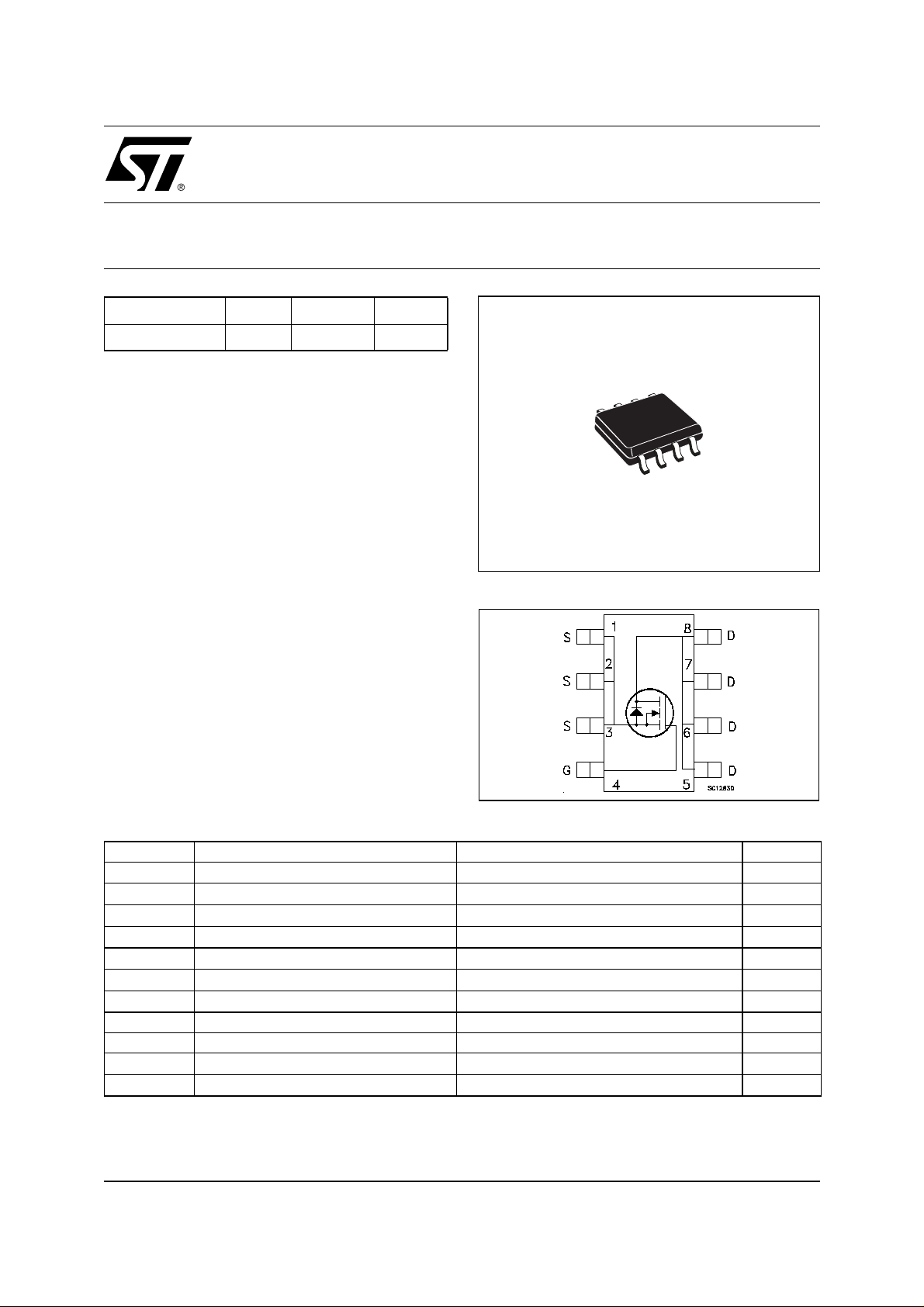
SO-8
INTERNAL SCHEMATIC DIAGRAM
ABSOLUTE MAXIMUM RATINGS
Symbol Parameter Value Unit
V
DS
V
DGR
V
GS
(
I
•)
D
I
D
(
I
••)
DM
P
tot
dV/dt
T
stg
T
j
(
Pulse wi dth limited by safe operating area.
••)
(
Current limited by the package
•)
NEW DATASHEET ACCORDING TO PCN DSG/CT/2C13 MARKING: 11NF30L@
Drain-source Voltage (VGS = 0)
Drain-gate Voltage (RGS = 20 kΩ)
30 V
30 V
Gate- source Voltage ± 18 V
Drain Current (continuous) at TC = 25°C
Drain Current (continuous) at TC = 100°C
11 A
7A
Drain Current (pulsed) 44 A
Total Dissipation at TC = 25°C
2.5 W
Derating Factor 0.02 W/°C
(1) Peak Diode Recovery voltage slope 5.5 V/ns
Storage Temperature -55 to 150 °C
Max. Operating Junction Temperature 150 °C
≤11A, di/dt ≤370A/ µ s , VDD ≤ V
(1) I
SD
(BR)DSS
, Tj ≤ T
JMAX
1/8September 2003
STS11NF30L
THERMA L D ATA
Rthj-amb
T
(*)
When Mounted on 1 inch2 FR-4 board, 2 oz of Cu and t [ 10 sec.
(*)
Thermal Resistance Junction-ambient
Maximum Lead Temperature For Soldering Purpose
l
Max
Typ
50
150
°C/W
°C
ELECTRICAL CHARACTERISTICS (T
= 25 °C unless otherwise specified)
case
OFF
Symbol Parameter Test Conditions Min. Typ. Max. Unit
= 250 µA, VGS = 0
I
D
= Max Rating
V
DS
V
= Max Rating TC = 125°C
DS
= ± 18 V
V
GS
30 V
1
10
±100 nA
ON
V
(BR)DSS
I
DSS
I
GSS
(1)
Drain-source
Breakdown Voltage
Zero Gate Voltage
Drain Current (V
GS
Gate-body Leakage
Current (V
DS
= 0)
= 0)
Symbol Parameter Test Conditions Min. Typ. Max. Unit
V
V
GS(th)
R
DS(on)
Gate Threshold Voltage
Static Drain-source On
Resistance
= VGS I
DS
= 10 V ID = 5.5 A
V
GS
V
= 5 V ID = 5.5 A
GS
= 250 µA
D
1V
0.0085
0.0145
0.0105
0.0190
DYNAMIC
Symbol Parameter Test Conditions Min. Typ. Max. Unit
(*)
g
fs
C
iss
C
oss
C
rss
Forward Transconductance
Input Capacitance
Output Capacitance
Reverse Transfer
Capacitance
V
=25V ID= 5.5 A
DS
= 25V, f = 1 MHz, VGS = 0
V
DS
15 S
1440
560
135
µA
µA
Ω
Ω
pF
pF
pF
2/8
STS11NF30L
ELECTRICAL CHARACTERISTICS (continued)
SWITCHING ON
Symbol Parameter Test Conditions Min. Typ. Max. Unit
= 15 V ID = 55 A
t
d(on)
Turn-on Delay Time
t
r
Rise Time
V
DD
R
= 4.7 Ω VGS = 5 V
G
(Resistive Load, Figure 3)
Q
g
Q
gs
Q
gd
Total Gate Charge
Gate-Source Charge
Gate-Drain Charge
= 15V ID= 11A VGS=5V
V
DD
SWITCHING OFF
Symbol Parameter Test Conditions Min. Typ. Max. Unit
= 15 V ID = 5.5 A
t
d(off)
Turn-off Delay Time
t
f
Fall Time
V
DD
R
= 4.7Ω, V
G
GS
= 5 V
(Resistive Load, Figure 3)
SOURCE DRAIN DIODE
Symbol Parameter Test Conditions Min. Typ. Max. Unit
I
SD
I
SDM
V
SD
t
rr
Q
rr
I
RRM
(*)
Pulsed: P ul se duration = 300 µs, duty cycle 1.5 %.
(
•)Pulse width limited by s afe operating area.
Source-drain Current
(•)
Source-drain Current (pulsed)
(*)
Forward On Voltage
Reverse Recovery Time
Reverse Recovery Charge
Reverse Recovery Current
I
= 11 A VGS = 0
SD
= 11 A di/dt = 100A/µs
I
SD
V
= 20 V Tj = 150°C
DD
(see test circuit, Figure 5)
22
39
22.5
9
12
23
16
42
52
2.5
30 nC
11
44
1.2 V
ns
ns
nC
nC
ns
ns
A
A
ns
nC
A
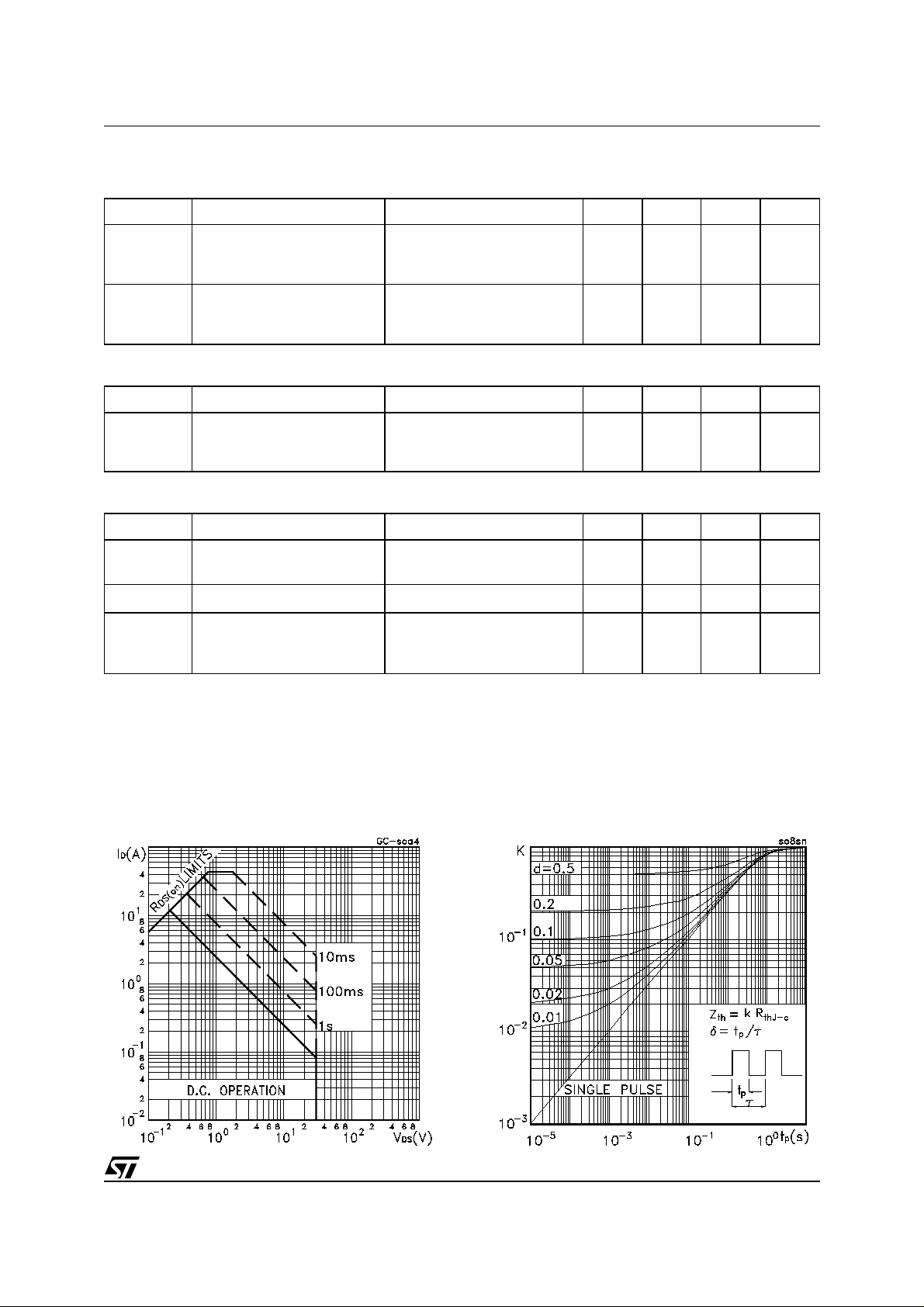
Safe Operating Area
Thermal Impedance
3/8
 Loading...