

ST STRH8N10 User Manual
Features
V
DSS
100 V 6 A 0.30 Ω 22 nC
■ Fast switching
■ 100% avalanche tested
■ Hermetic package
■ 70 krad TID
■ SEE radiation hardened
I
D
R
DS(on)
Applications
■ Satellite
■ High reliability
STRH8N10
Rad-Hard N-channel 100 V, 6 A
Power MOSFET
Q
g
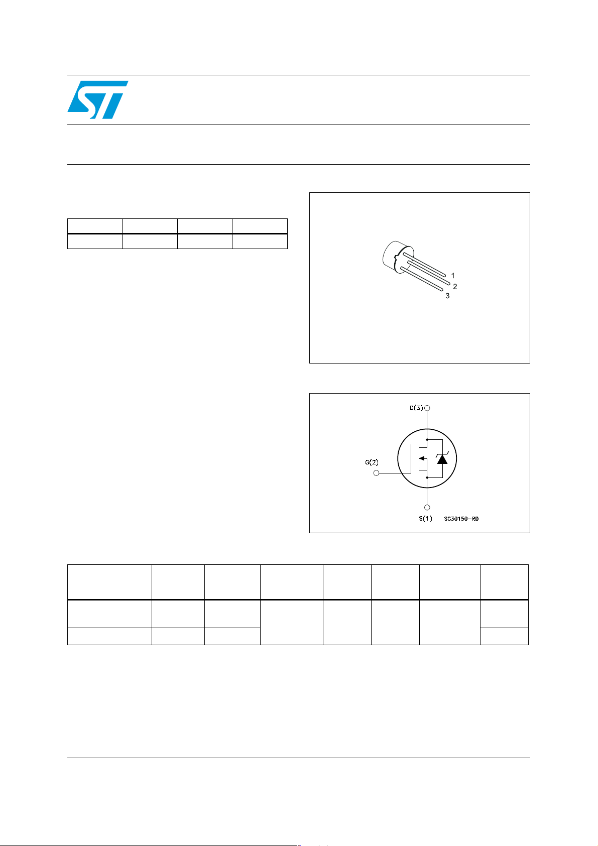
TO-39
Figure 1. Internal schematic diagram
Description
This N-channel Power MOSFET is developed with
STMicroelectronics unique STripFET
has specifically been designed to sustain high
TID and provide immunity to heavy ion effects.
Table 1. Device summary
Order code
STRH8N10N1 -
STRH8N10NG TBD ESCC flight Target
ESCC part
number
Note: Contact ST sales office for information about the specific conditions for product in die form
and for other packages.
™
process. It
Quality
level
Engineering
model
Package
TO-39 Gold 1.2 -55 to 150°C
Lead
finish
Mass
(g)
Temp. range EPPL
-
November 2011 Doc ID 010029 Rev 2 1/18
www.st.com
18

Contents STRH8N10
Contents
1 Electrical ratings . . . . . . . . . . . . . . . . . . . . . . . . . . . . . . . . . . . . . . . . . . . . 3
2 Electrical characteristics . . . . . . . . . . . . . . . . . . . . . . . . . . . . . . . . . . . . . 5
2.1 Pre-irradiation . . . . . . . . . . . . . . . . . . . . . . . . . . . . . . . . . . . . . . . . . . . . . . . 5
3 Radiation characteristics . . . . . . . . . . . . . . . . . . . . . . . . . . . . . . . . . . . . . 7
4 Electrical characteristics (curves) . . . . . . . . . . . . . . . . . . . . . . . . . . . . . 10
5 Test circuit . . . . . . . . . . . . . . . . . . . . . . . . . . . . . . . . . . . . . . . . . . . . . . . . 12
6 Package mechanical data . . . . . . . . . . . . . . . . . . . . . . . . . . . . . . . . . . . . 14
7 Order codes . . . . . . . . . . . . . . . . . . . . . . . . . . . . . . . . . . . . . . . . . . . . . . . 16
8 Revision history . . . . . . . . . . . . . . . . . . . . . . . . . . . . . . . . . . . . . . . . . . . 17
2/18 Doc ID 010029 Rev 2
STRH8N10 Electrical ratings
1 Electrical ratings
(TC = 25°C unless otherwise specified)
Table 2. Absolute maximum ratings (pre-irradiation)
Symbol Parameter Value Unit
(1)
V
DS
V
GS
I
D
I
D
I
DM
P
TOT
dv/dt
T
1. This rating is guaranteed @ TJ > 25 °C (see Figure 10: Normalized BV
2. This value is guaranteed over the full range of temperature.
3. Rated according to the Rthj-case + Rthc-s.
4. Pulse width limited by safe operating area.
5. ISD ≤ 6 A, di/dt ≤ 1060 A/µs, VDD = 80% V
Drain-source voltage (VGS = 0)
(2)
Gate-source voltage ±20 V
(3)
Drain current (continuous) at TC= 25°C 6 A
(1)
Drain current (continuous) at TC= 100°C 4.1 A
(4)
Drain current (pulsed) 24 A
(1)
Total dissipation at TC= 25°C 25 W
(5)
Peak diode recovery voltage slope 6.4 V/ns
Storage temperature -55 to 150 °C
stg
T
Max. operating junction temperature 150 °C
j
(BR)DSS
DSS
100 V
vs temperature).
Table 3. Thermal data
Symbol Parameter Value Unit
Rthj-case Thermal resistance junction-case 5.0 °C/W
Table 4. Avalanche characteristics
Symbol Parameter Value Unit
I
E
AS
E
Avalanche current, repetitive or not-repetitive
AR
(pulse width limited by Tj Max)
Single pulse avalanche energy
(1)
(starting Tj=25°C, Id=Iar, Vdd=50V)
Single pulse avalanche energy
AS
(starting Tj=110°C, Id=Iar, Vdd=50V)
4A
457 mJ
134 mJ
Doc ID 010029 Rev 2 3/18

Electrical ratings STRH8N10
Table 4. Avalanche characteristics (continued)
Symbol Parameter Value Unit
Repetitive avalanche
E
AR
(Vdd = 50 V, I
duty cycle = 10%)
Repetitive avalanche
E
(Vdd = 50 V, IAR = 4 A, f = 100 KHz, TJ = 110 °C,
AR
duty cycle = 10%)
1. Maximum rating value.
= 4 A, f = 100 KHz, TJ = 25 °C,
AR
4.3 mJ
1.4 mJ
4/18 Doc ID 010029 Rev 2
STRH8N10 Electrical characteristics
2 Electrical characteristics
(T
= 25°C unless otherwise specified).
CASE
2.1 Pre-irradiation
Table 5. On/off states
Symbol Parameter Test conditions Min. Typ. Max. Unit
I
I
V
GS(th)
R
DS(on)
DSS
GSS
Zero gate voltage drain
current (V
Gate body leakage current
= 0)
(V
DS
Gate threshold voltage
Static drain-source on
resistance
GS
= 0)
100% BV
80% BV
80% BV
V
GS
V
GS
V
GS
V
GS
V
DS
V
DS
Dss
Dss
Dss, TC
= 20 V
= -20 V
= 20 V, TC = 125 °C
= -20 V, TC = 125 °C
=VGS, ID = 1mA
=VGS, ID = 1mA
TC = 125 °C
=VGS, ID = 1mA
V
DS
TC = -55 °C
V
= 12 V, ID = 4 A
GS
= 12 V, ID = 4 A,
V
GS
TC = 125 °C
= 125 °C
,
,
-100
-200
2
1.5
2.1
1mA
10
100
µA
100
200
nA
4.5
3.7
V
5.5
0.30
0.72
Ω
Table 6. Dynamic
Symbol Parameter Test conditions Min. Typ. Max. Unit
C
C
oss
C
C
oss eq.
Q
Q
Q
R
1. This value is guaranteed over the full range of temperature.
2. This value is defined as the ratio between the Q
3. Not tested, guaranteed by process.
Input capacitance
iss
Output capacitance
(1)
Reverse transfer
rss
capacitance
Equivalent output
(1)
capacitance
Total gate charge
g
Gate-to-source charge
gs
Gate-to-drain (“Miller”)
gd
charge
(3)
Gate input resistance
G
(2)
= 25 V, f=1 MHz,
V
DS
=0V
V
GS
527
76
31
659
95
39
791
114
47
VDD = 80 V, VGS=0V 162 pF
= 50 V, ID = 4 A,
V
DD
= 12 V
V
GS
18.5
3
4
5.5
22
4
5
7
15
f=1MHz gate DC bias=0
test signal level=20mV
1.6 Ω
open drain
and the voltage value applied.
oss
Doc ID 010029 Rev 2 5/18
pF
pF
pF
nC
nC
nC
Electrical characteristics STRH8N10
Table 7. Switching times
Symbol Parameter Test conditions Min. Typ. Max Unit
t
d(on)
t
d(off)
Turn-on delay time
t
Rise time
r
Turn-off-delay time
t
Fall time
f
Table 8. Source drain diode
= 50 V, ID = 4 A,
V
DD
RG = 4.7 Ω, VGS = 12 V
(1)
6
4
13
3
10.5
10.5
21.5
5.5
15
17
30
8
Symbol Parameter Test conditions Min. Typ. Max Unit
I
I
SDM
V
SD
t
rr
Q
I
RRM
t
rr
Q
I
RRM
1. Refer to the Figure 16: Source drain diode.
2. Pulse width limited by safe operating area.
3. Pulsed: pulse duration = 300 µs, duty cycle 1.5%
4. Not tested in production, guaranteed by process.
Source-drain current
SD
(2)
Source-drain current (pulsed)
(3)
Forward on voltage
(4)
Reverse recovery time
(4)
Reverse recovery charge
rr
(4)
Reverse recovery current
(4)
Reverse recovery time
(4)
Reverse recovery charge
rr
(4)
Reverse recovery current
= 8 A, VGS = 0
I
SD
= 8 A, VGS = 0,
I
SD
TC = 125 °C
= 8 A, di/dt = 100
I
SD
A/µs
= 17 V, Tj = 25 °C
V
DD
= 8 A,
I
SD
di/dt = 100 A/µs, VDD=
17 V, Tj = 150 °C
196 245
1.2
10
282 352
1.7
10.5
6
24
1.5
1.275
294 ns
422 ns
ns
ns
ns
ns
A
A
V
µC
A
µC
A
6/18 Doc ID 010029 Rev 2
 Loading...