


ST STRH40P10 User Manual
Rad-Hard P-channel 100 V, 34 A Power MOSFET
Features
V
BDSS
100 V 34 A 0.060 Ohm 162 nC
■ Fast switching
■ 100% avalanche tested
■ Hermetic package
■ 100 krad TID
■ SEE radiation hardened
I
D
R
DS(on)
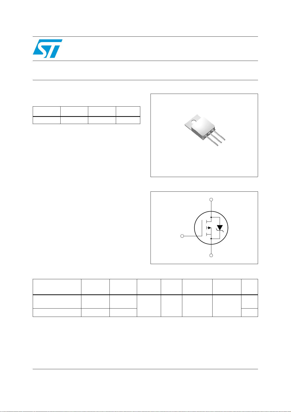
STRH40P10
Q
g
3
2
TO-254AA
1
Applications
■ Satellite
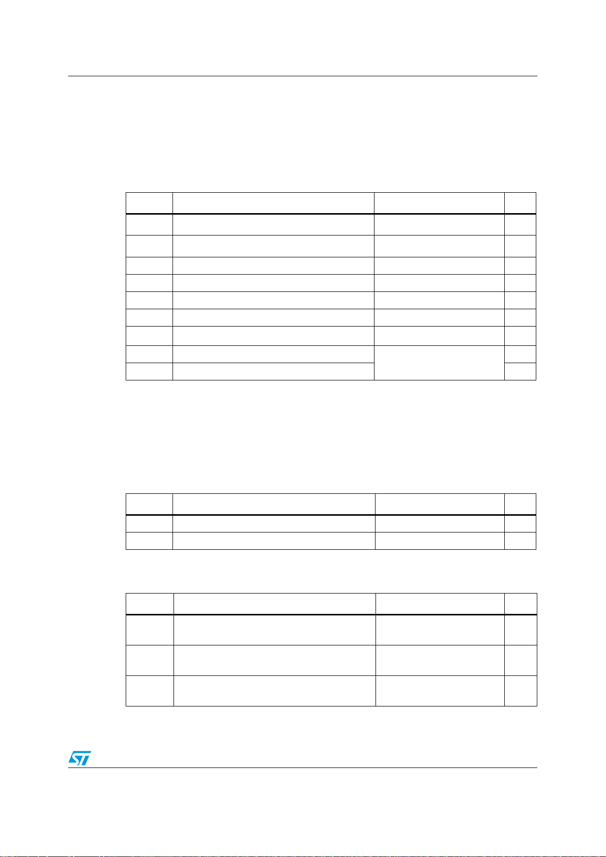
Figure 1. Internal schematic diagram
■ High reliability
D (1)
Description
This P-channel Power MOSFET is developed with
STMicroelectronics unique STripFET™ process.
It has specifically been designed to sustain high
TID and provide immunity to heavy ion effects.
Table 1. Device summary
Part number
ESCC part
number
STRH40P10HY1 -
STRH40P10HYG TBD ESCC flight Target
Quality
level
Engineering
model
Package
Lead
finish
TO-254AA Gold 10 -55 to 150°C
G (3)
SC06140p
S (2)
Mass (g) Temp. range EPPL
-
Note: Contact ST sales office for information about the specific conditions for product in die form
and for other packages.
November 2011 Doc ID 18354 Rev 6 1/18
www.st.com
18

Contents STRH40P10
Contents
1 Electrical ratings . . . . . . . . . . . . . . . . . . . . . . . . . . . . . . . . . . . . . . . . . . . . 3
2 Electrical characteristics . . . . . . . . . . . . . . . . . . . . . . . . . . . . . . . . . . . . . 5
3 Radiation characteristics . . . . . . . . . . . . . . . . . . . . . . . . . . . . . . . . . . . . . 7
4 Electrical characteristics (curves) . . . . . . . . . . . . . . . . . . . . . . . . . . 10
5 Test circuits . . . . . . . . . . . . . . . . . . . . . . . . . . . . . . . . . . . . . . . . . . . . . . . 12
6 Package mechanical data . . . . . . . . . . . . . . . . . . . . . . . . . . . . . . . . . . . . 13
7 Order codes . . . . . . . . . . . . . . . . . . . . . . . . . . . . . . . . . . . . . . . . . . . . . . . 16
8 Revision history . . . . . . . . . . . . . . . . . . . . . . . . . . . . . . . . . . . . . . . . . . . 17
2/18 Doc ID 18354 Rev 6
STRH40P10 Electrical ratings
1 Electrical ratings
(TC= 25 °C unless otherwise specified).
Note: For the P-channel MOSFET actual polarity of voltages and current has to be reversed.
Table 2. Absolute maximum ratings (pre-irradiation)
Symbol Parameter Value Unit
(1)
V
DS
V
GS
I
D
I
D
I
DM
P
TOT
dv/dt
T
T
Drain-source voltage (VGS = 0)
(2)
Gate-source voltage ±20 V
(3)
Drain current (continuous) 34 A
(3)
Drain current (continuous) at TC= 100 °C 21 A
(4)
Drain current (pulsed) 136 A
(3)
Total dissipation 176 W
(5)
Peak diode recovery voltage slope 2.5 V/ns
Storage temperature
stg
Operating junction temperature °C
J
1. This rating is guaranteed @ TJ ≥ 25 °C (see Figure 10: Normalized BV
2. This value is guaranteed over the full range of temperature.
3. Rated according to the Rthj-case + Rthc-s.
4. Pulse width limited by safe operating area.
5. ISD ≤ 40 A, di/dt ≤ 100 A/µs, VDD = 80% V
(BR)DSS.
DSS
100 V
°C
- 55 to 150
vs temperature).
Table 3. Thermal data
Symbol Parameter Value Unit
R
thj-case
R
thc-s
Thermal resistance junction-case max 0.71 °C/W
Case-to-sink typ 0.21 °C/W
Table 4. Avalanche characteristics
Symbol Parameter Value Unit
I
E
AS
E
Avalanche current, repetitive or not-repetitive
AR
(pulse width limited by T
Single pulse avalanche energy
(1)
(starting T
=25 °C, ID= 17 A, VDD=50 V)
J
max)
J
Single pulse avalanche energy
AS
(starting T
=110 °C, ID= 17 A, VDD=50 V)
J
Doc ID 18354 Rev 6 3/18
TBD A
1133 mJ
332 mJ

Electrical ratings STRH40P10
Table 4. Avalanche characteristics (continued)
Symbol Parameter Value Unit
Repetitive avalanche
= 50 V, IAR = 24 A, f = 100 KHz, TJ = 25 °C,
(V
dd
duty cycle = 10%)
E
AR
Repetitive avalanche
= 50 V, IAR = 17 A, f = 100 KHz, TJ = 110
(V
dd
°C, duty cycle = 10%)
1. Maximum rating value.
25
mJ
8
4/18 Doc ID 18354 Rev 6
STRH40P10 Electrical characteristics
2 Electrical characteristics
(TC = 25 °C unless otherwise specified).
Note: For the P-channel MOSFET actual polarity of voltages and current has to be reversed.
Pre-irradiation
Table 5. Pre-irradiation on/off states
Symbol Parameter Test conditions Min. Typ. Max. Unit
I
DSS
I
GSS
BV
DSS
V
GS(th)
R
DS(on)
1. This rating is guaranteed @ TJ ≥ 25 °C (see Figure 10: Normalized BV
Table 6. Pre-irradiation dynamic
Zero gate voltage drain
current (V
GS
= 0)
Gate body leakage current
= 0)
(V
DS
Drain-to-source breakdown
(1)
voltage
80% BV
V
V
V
Dss
= 20 V
GS
= -20 V -100
GS
= 0, ID = 1 mA 100 V
GS
100 nA
Gate threshold voltage VDS = VGS, ID = 1 mA 2 4.5 V
Static drain-source on
resistance
= 12 V; ID = 17 A 0.060 0.075 Ω
V
GS
vs temperature).
DSS
10 µA
Symbol Parameter Test conditions Min. Typ. Max. Unit
C
C
oss
C
Q
Q
Q
Input capacitance
iss
Output capacitance
(1)
Reverse transfer
rss
capacitance
Total gate charge
g
Gate-to-source charge
gs
Gate-to-drain (“Miller”)
gd
charge
= 0, VDS = 25 V,
V
GS
f=1 MHz
= 50 V, ID = 34 A,
V
DD
=12 V
V
GS
3710
510
204
130
14
32
4640
635
255
162
18
40
5570
760
306
194
22
48
nA
pF
pF
pF
nC
nC
nC
(1)
R
Gate input resistance
G
test signal level=20mV
1.5 Ω
open drain
f=1MHz gate DC bias=0
1. Not tested, guaranteed by process.
Table 7. Pre-irradiation switching times
Symbol Parameter T e st cond itions Min. Typ. Max Unit
t
d(on)
t
d(off)
Turn-on delay time
t
Rise time
r
Turn-off-delay time
t
Fall time
f
= 50 V, ID = 17 A,
V
DD
R
= 4.7 Ω, VGS = 12 V
G
15
19
68
34
24
31
129
46
33
43
190
58
ns
ns
ns
ns
Doc ID 18354 Rev 6 5/18

Electrical characteristics STRH40P10
Table 8. Pre-irradiation source drain diode
(1)
Symbol Parameter Test conditions Min. Typ. Max Unit
I
I
SDM
V
SD
t
rr
Q
I
RRM
t
rr
Q
I
RRM
1. Refer to the Figure 16.
2. Pulse width limited by safe operating area.
3. Pulsed: pulse duration = 300 µs, duty cycle 1.5%.
4. Not tested in production, guaranteed by process.
Source-drain current
SD
Source-drain current
(2)
(pulsed)
(3)
Forward on voltage I
(4)
Reverse recovery time
(4)
Reverse recovery charge
rr
(4)
Reverse recovery current
(4)
Reverse recovery time
(4)
Reverse recovery charge
rr
(4)
Reverse recovery current
34
136
= 30 A, VGS = 0 1.1 V
SD
= 34 A,
I
SD
di/dt = 40 A/µs
= 12 V, TJ = 25 °C
V
DD
= 34 A,
I
SD
di/dt = 40 A/µs
= 12 V, TJ = 150 °C
V
DD
276 345
316
473
133
414 ns
4.1
7.1
A
A
µC
A
ns
µC
A
6/18 Doc ID 18354 Rev 6