

ST STR730FZ1, STR730FZ2, STR731FV0, STR731FV1, STR731FV2 User Manual
...
ARM7TDMI™ 32-bit MCU with Flash, 3x CAN,
TQFP144
20 x 20
TQFP100 14 x 14
LFBGA144 10 x 10 x 1.7
4 UARTs, 20 timers, ADC, 12 comm. interfaces
Features
■ Core
– ARM7TDMI 32-bit RISC CPU
– 32 MIPS @ 36 MHz
■ Memories
– Up to 256 Kbytes Flash program memory
(10,000 cycles endurance, data retention
20 years @ 85° C)
– 16 Kbytes RAM
■ Clock, reset and supply management
– 4.5 - 5.5 V application supply and I/Os
– Embedded 1.8 V regulator for core supply
– Embedded oscillator running from external
4-8 MHz crystal or ceramic resonator
– Up to 36 MHz CPU frequency with internal
PLL
– 32 kHz or 2 MHz internal RC oscillator,
software configurable for fast startup and
backup clock
– Real-time clock for clock-calendar function
– Wake-up timer driven by internal RC for
wake-up from STOP mode
– 5 power saving modes: SLOW, WFI,
LPWFI, STOP and HALT modes
■ Nested interrupt controller
– Fast interrupt handling with multiple vectors
– 64 maskable IRQs with 64 vectors and 16
priority levels
– 2 maskable FIQ sources
– 16 external interrupts, up to 32 wake-up
lines
■ Up to 112 I/O ports
– 72/112 multifunctional bidirectional I/Os
STR73xFxx
■ DMA
– 4 DMA controllers with 4 channels each
■ Timers
– 16-bit watchdog timer (WDG)
– 6/10 16-bit timers (TIM) each with: 2 input
captures, 2 output compares, PWM and
pulse counter modes
– 6 16-bit PWM modules (PWM)
– 3 16-bit timebase timers with 8-bit
prescalers
■ 12 communications interfaces
2
–2 I
C interfaces
– 4 UART asynchronous serial interfaces
– 3 BSPI synchronous serial interfaces
–Up to 3 CAN interfaces (2.0B Active)
■ 10-bit A/D converter
– 12/16 channels
– Conversion time: min. 3 µs, range: 0 to 5V
■ Development tools support
–JTAG interface
Table 1. Device summary
Reference Part number
STR730FZ1, STR730FZ2,
STR731FV0, STR731FV1,
STR73xFxx
STR731FV2,
STR735FZ1, STR735FZ2,
STR736FV0, STR736FV1,
STR736FV2
June 2008 Rev 7 1/52
www.st.com
52

Contents STR73xFxx
Contents
1 Scope . . . . . . . . . . . . . . . . . . . . . . . . . . . . . . . . . . . . . . . . . . . . . . . . . . . . . 4
1.1 Description . . . . . . . . . . . . . . . . . . . . . . . . . . . . . . . . . . . . . . . . . . . . . . . . . 4
2 Overview . . . . . . . . . . . . . . . . . . . . . . . . . . . . . . . . . . . . . . . . . . . . . . . . . . 5
2.1 On-chip peripherals . . . . . . . . . . . . . . . . . . . . . . . . . . . . . . . . . . . . . . . . . . 6
3 Block diagram . . . . . . . . . . . . . . . . . . . . . . . . . . . . . . . . . . . . . . . . . . . . . . 8
3.1 Related documentation . . . . . . . . . . . . . . . . . . . . . . . . . . . . . . . . . . . . . . 10
3.2 Pin description . . . . . . . . . . . . . . . . . . . . . . . . . . . . . . . . . . . . . . . . . . . . . 11
3.2.1 STR730F/STR735F (TQFP144) . . . . . . . . . . . . . . . . . . . . . . . . . . . . . . 11
3.2.2 STR730F/STR735F (LFBGA144) . . . . . . . . . . . . . . . . . . . . . . . . . . . . . 12
3.2.3 STR731F/STR736F (TQFP100) . . . . . . . . . . . . . . . . . . . . . . . . . . . . . . 13
3.3 Memory mapping . . . . . . . . . . . . . . . . . . . . . . . . . . . . . . . . . . . . . . . . . . . 20
4 Electrical parameters . . . . . . . . . . . . . . . . . . . . . . . . . . . . . . . . . . . . . . . 21
4.1 Parameter conditions . . . . . . . . . . . . . . . . . . . . . . . . . . . . . . . . . . . . . . . . 21
4.1.1 Minimum and maximum values . . . . . . . . . . . . . . . . . . . . . . . . . . . . . . . 21
4.1.2 Typical values . . . . . . . . . . . . . . . . . . . . . . . . . . . . . . . . . . . . . . . . . . . . . 21
4.1.3 Typical curves . . . . . . . . . . . . . . . . . . . . . . . . . . . . . . . . . . . . . . . . . . . . 21
4.1.4 Loading capacitor . . . . . . . . . . . . . . . . . . . . . . . . . . . . . . . . . . . . . . . . . 21
4.1.5 Pin input voltage . . . . . . . . . . . . . . . . . . . . . . . . . . . . . . . . . . . . . . . . . . 21
4.2 Absolute maximum ratings . . . . . . . . . . . . . . . . . . . . . . . . . . . . . . . . . . . . 22
4.3 Operating conditions . . . . . . . . . . . . . . . . . . . . . . . . . . . . . . . . . . . . . . . . 24
4.3.1 Supply current characteristics . . . . . . . . . . . . . . . . . . . . . . . . . . . . . . . . 25
4.3.2 Clock and timing characteristics . . . . . . . . . . . . . . . . . . . . . . . . . . . . . . 29
4.3.3 Memory characteristics . . . . . . . . . . . . . . . . . . . . . . . . . . . . . . . . . . . . . 34
4.3.4 EMC characteristics . . . . . . . . . . . . . . . . . . . . . . . . . . . . . . . . . . . . . . . . 35
4.3.5 I/O port pin characteristics . . . . . . . . . . . . . . . . . . . . . . . . . . . . . . . . . . . 38
4.3.6 10-bit ADC characteristics . . . . . . . . . . . . . . . . . . . . . . . . . . . . . . . . . . . 43
5 Package characteristics . . . . . . . . . . . . . . . . . . . . . . . . . . . . . . . . . . . . . 46
5.1 Package mechanical data . . . . . . . . . . . . . . . . . . . . . . . . . . . . . . . . . . . . 46
5.2 Thermal characteristics . . . . . . . . . . . . . . . . . . . . . . . . . . . . . . . . . . . . . . 48
2/52

STR73xFxx Contents
6 Order codes . . . . . . . . . . . . . . . . . . . . . . . . . . . . . . . . . . . . . . . . . . . . . . . 49
7 Known limitations . . . . . . . . . . . . . . . . . . . . . . . . . . . . . . . . . . . . . . . . . . 50
7.1 Low power wait for interrupt mode . . . . . . . . . . . . . . . . . . . . . . . . . . . . . . 50
7.2 PLL free running mode at high temperature . . . . . . . . . . . . . . . . . . . . . . 50
8 Revision history . . . . . . . . . . . . . . . . . . . . . . . . . . . . . . . . . . . . . . . . . . . 51
3/52

Scope STR73xFxx
1 Scope
This datasheet provides the STR73x ordering information, mechanical and electrical device
characteristics.
For complete information on the STR73xF microcontroller memory, registers and
peripherals. please refer to the STR73x reference manual.
For information on programming, erasing and protection of the internal Flash memory
please refer to the STR7 Flash programming reference manual.
For information on the ARM7TDMI core please refer to the ARM7TDMI technical reference
manual.
1.1 Description
ARM core with embedded Flash & RAM
STR73xF family combines the high performance ARM7TDMI
of peripheral functions and enhanced I/O capabilities. All devices have on-chip high-speed
single voltage Flash memory and high-speed RAM. The STR73xF family has an embedded
ARM core and is therefore compatible with all ARM tools and software.
™
CPU with an extensive range
Extensive tools support
STMicroelectronics’ 32-bit, ARM core-based microcontrollers are supported by a complete
range of high-end and low-cost development tools to meet the needs of application
developers. This extensive line of hardware/software tools includes starter kits and complete
development packages all tailored for ST’s ARM core-based MCUs.
The range of development packages includes third-party solutions that come complete with
a graphical development environment and an in-circuit emulator/programmer featuring a
JTAG application interface. These support a range of embedded operating systems (OS),
while several royalty-free OSs are also available.
For more information, please refer to ST MCU site http://www.st.com/mcu
Figure 1 shows the general block diagram of the device family.
4/52
STR73xFxx Overview
2 Overview
Table 2. Product overview
Flash memory - bytes 128K 256K 128K 256K 64K 128K 256K 64K 128K 256K
Peripheral functions
CAN peripherals 3 0 3 0
Operating voltage 4.5 to 5.5 V
Operating temperature -40 to +85°C/-40 to +105° C
Features STR730FZx STR735FZx STR731FVx STR736FVx
RAM - bytes 16 K 16 K
Packages
10 TIM timers, 112 I/Os,
32 wake-up lines, 16 ADC
T=TQFP144 20 x 20
H=LFBGA144 10 x10
6 TIM timers, 72 I/Os, 18 wake-up lines,
12 ADC channels
T=TQFP100 14x14
Package choice: reduced pin-count TQFP100 or feature-rich 144-pin TQFP or LFBGA
The STR73xF family is available in 3 packages. The TQFP144 and LFBGA144 versions
have the full set of all features. The 100-pin version has fewer timers, I/Os and ADC
channels. Refer to the Device Summary on Page 1 for a comparison of the I/Os available on
each package.
The family includes versions with and without CAN.
High speed Flash memory
The Flash program memory is organized in 32-bit wide memory cells which can be used for
storing both code and data constants. It is accessed by CPU with zero wait states @ 36
MHz.
The STR7 embedded Flash memory can be programmed using in-circuit programming or
in-application programming.
The Flash memory endurance is 10K write/erase cycles and the data retention is 20 years
@ 85° C.
IAP (in-application programming): IAP is the ability to re-program the Flash memory of a
microcontroller while the user program is running.
ICP (in-circuit programming): ICP is the ability to program the Flash memory of a
microcontroller using JTAG protocol while the device is mounted on the user application
board.
The Flash memory can be protected against different types of unwanted access
(read/write/erase). There are two types of protection:
● Sector write protection
● Flash debug protection (locks JTAG access)
Flexible power management
To minimize power consumption, you can program the STR73xF to switch to SLOW, WFI
LPWFI, STOP or HALT modes depending on the current system activity in the application.
5/52

Overview STR73xFxx
Flexible clock control
Two clock sources are used to drive the microcontroller, a main clock driven by an external
crystal or ceramic resonator and an internal backup RC oscillator that operates at 2 MHz or
32 kHz. The embedded PLL can be configured to generate an internal system clock of up to
36 MHz. The PLL output frequency can be programmed using a wide selection of multipliers
and dividers.
Voltage regulators
The STR73xF requires an external 4.5 to 5.5 V power supply. There are two internal Voltage
Regulators for generating the 1.8 V power supply needed by the core and peripherals. The
main VR is switched off and the Low Power VR switched on when the application puts the
STR73xF in Low Power Wait for Interrupt (LPWFI) mode.
Low voltage detectors
The voltage regulator and Flash modules each have an embedded LVD that monitors the
internal 1.8 V supply. If the voltage drops below a certain threshold, the LVD will reset the
STR73xF.
Note: An external power-on reset must be provided ensure the microcontroller starts-up correctly.
2.1 On-chip peripherals
CAN interfaces
The three CAN modules are compliant with the CAN specification V2.0 part B (active). The
bit rate can be programmed up to 1 MBaud. These are not available in the STR735 and
STR736.
DMA
4 DMA controllers, each with 4 data streams manage memory to memory, peripheral to
peripheral, peripheral to memory and memory to peripheral transfers. The DMA requests
are connected to TIM timers, BSPI0, BSPI1, BSPI2 and ADC. One of the streams can be
configured to be triggered by a software request, independently from any peripheral activity.
16-bit timers (TIM)
Each of the ten timers (six in 100-pin devices) have a 16-bit free-running counter with 7-bit
prescaler, up to two input capture/output compare functions, a pulse counter function, and a
PWM channel with selectable frequency. This provides a total of 16 independent PWMs (12
in 100-pin devices) when added with the PWM modules (see next paragraph).
PWM modules (PWM)
The six 16-bit PWM modules have independently programmable periods and duty-cycles,
with 5+3 bit prescaler factor.
Timebase timers (TB)
The three 16-bit timebase timers with 8-bit prescaler for general purpose time triggering
operations.
Real-time clock (RTC)
The RTC provides a set of continuously running counters driven by separate clock signal
derived from the main oscillator. The RTC can be used as a general timebase or
6/52

STR73xFxx Overview
clock/calendar/alarm function. When the STR73xF is in LPWFI mode the RTC keeps
running, powered by the low power voltage regulator.
UARTs
The 4 UARTs allow full duplex, asynchronous, communications with external devices with
independently programmable TX and RX baud rates up to 625 Kbaud.
Buffered serial peripheral interfaces (BSPI)
Each of the three BSPIs allow full duplex, synchronous communications with external
devices, master or slave communication at up to 6 Mb/s in master mode and up to 4.5 Mb/s
in slave mode (@36 MHz system clock).
2
I
C interfaces
The two I
2
I
C mode (400 kHz) and 7 or 10-bit addressing modes.
2
C Interfaces provide multi-master and slave functions, support normal and fast
A/D converter
The 10-bit analog to digital converter, converts up to 16 channels in single-shot or
continuous conversion modes (12 channels in 100-pin devices). The minimum conversion
time is 3 µs.
Watchdog
The 16-bit watchdog timer protects the application against hardware or software failures and
ensures recovery by generating a reset.
I/O ports
Up to 112 I/O ports (72 in 100-pin devices) are programmable as general purpose
input/output or alternate function.
External interrupts and wake-up lines
16 external interrupts lines are available for application use. In addition, up to 32 external
Wake-up lines (18 in 100-pin devices) can be used as general purpose interrupts or to
wake-up the application from STOP mode.
7/52
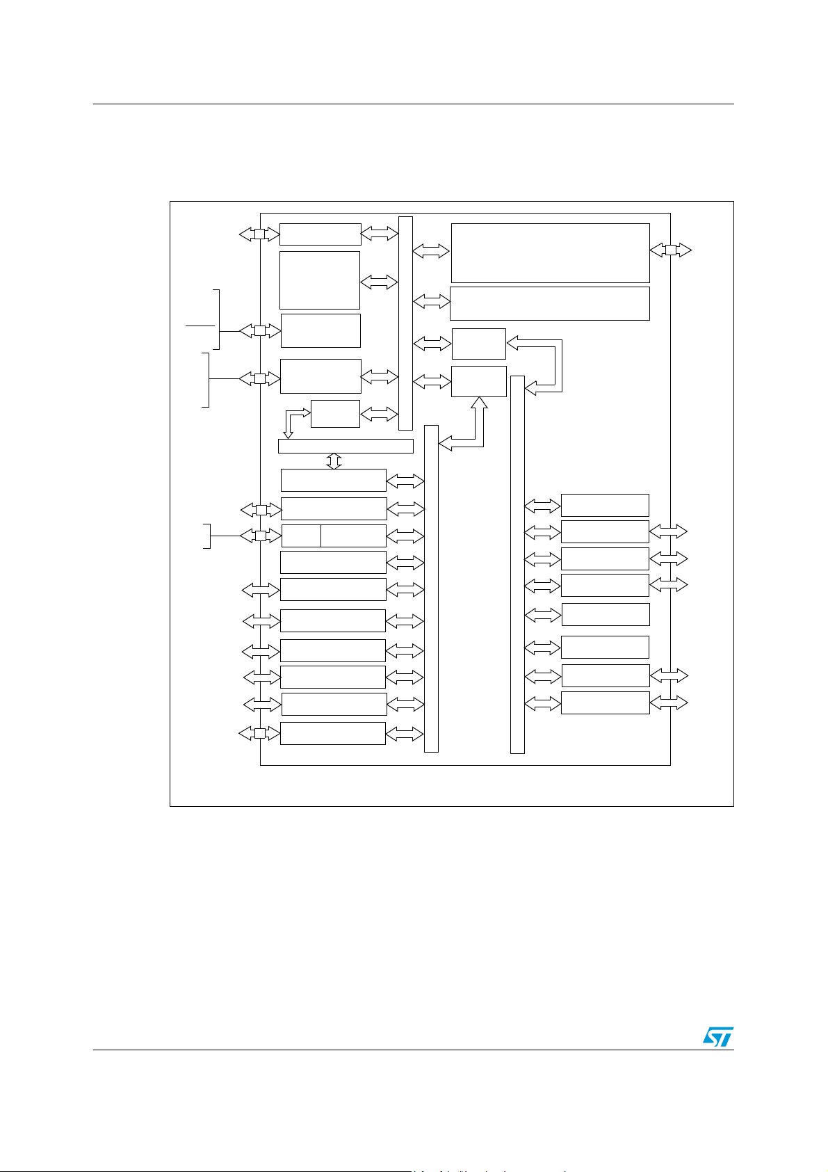
Block diagram STR73xFxx
APB BUS
122 ports
GPIO PORTS 0-6
WATCHDOG
I2C0-1
WAKE-UP/INT (WIU)
UART0, 1, 2, 3
WAKE-UP TIMER
APB BUS
BSPI 0-2
RTC
CAN 0-2*
INTERRUPT CTL (EIC)
A/D CONVERTER (ADC)
32 AF
8 AF
16 AF
12 AF
XTAL1
XTAL2
OSC
TIMER (TIM) 2-4
4 AF
AF: alternate function on I/O port pin
PWM 0-5
CLOCK MGT (CMU)
TIMER (TIM) 0-1
8 AF
TIMER (TIM) 5-9
20 AF
6 AF
(WUT)
TIMEBASE TIMER
(TB) 0-2
6 AF
12 AF
*CAN peripherals not available on STR735F.
FLASH
PROGRAM MEMORY
64/128/256K
APB
BRIDGE 0
APB
BRIDGE 1
POWER SUPPLY
PRCCU/PLL
RAM
16K
JTAG
ARM7TDMI
CPU
JTDI
JTCK
JTMS
JTRST
JTDO
RSTIN
V18
VDD
VSS
VREG
VDDA
VSSA
ARM7 NATIVE BUS
DMA0-3
AHB BUS
AHB
BRIDGE
M0
M1
TEST
3 Block diagram
Figure 1. STR730F/STR735F block diagram
8/52
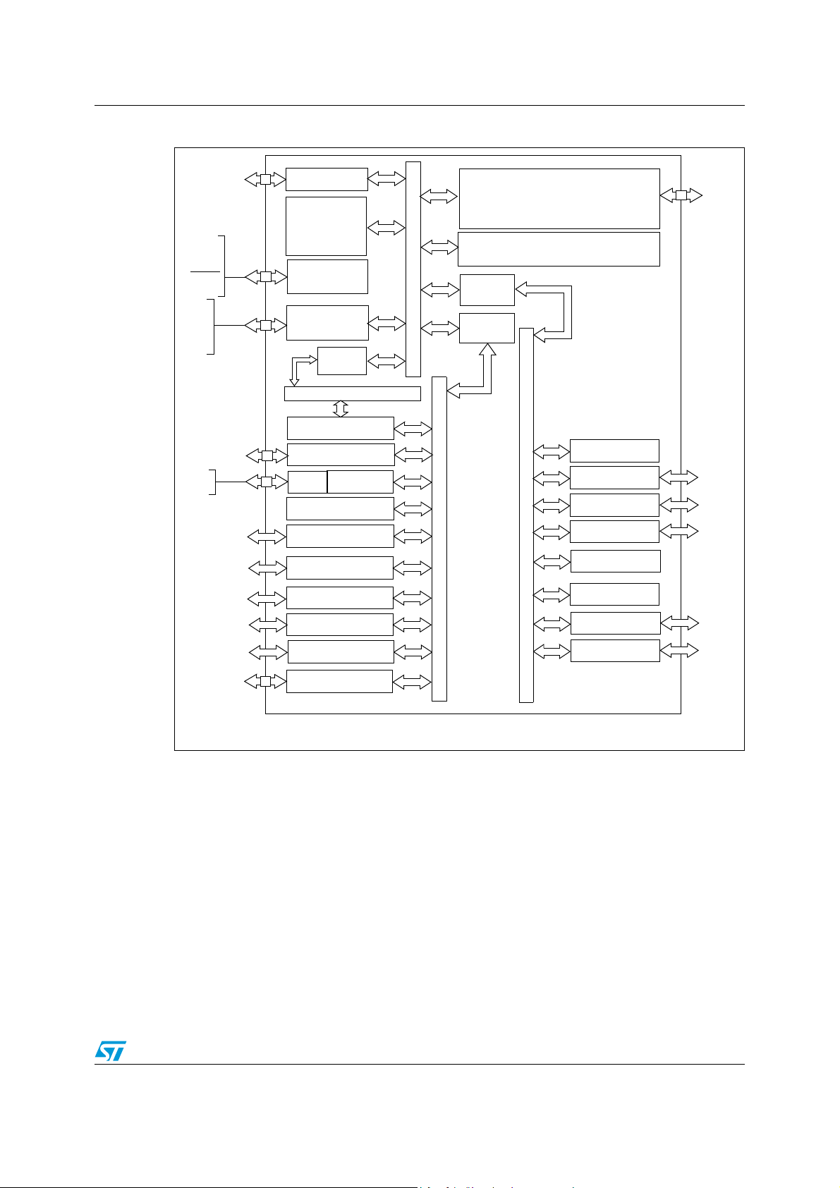
STR73xFxx Block diagram
APB BUS
72 ports
GPIO PORTS 0-6
FLASH
PROGRAM MEMORY
64/128/256K
WATCHDOG
I2C0-1
WAKE-UP/INT (WIU)
UART0, 1, 2, 3
WAKE-UP TIMER
APB
BRIDGE 0
APB
BRIDGE 1
APB BUS
BSPI 0-2
RTC
CAN 0-2*
INTERRUPT CTL (EIC)
A/D CONVERTER (ADC)
POWER SUPPLY
PRCCU/PLL
RAM
16K
JTAG
ARM7TDMI
CPU
18 AF
8 AF
12 AF
12 AF
XTAL1
XTAL2
JTDI
JTCK
JTMS
JTRST
JTDO
RSTIN
V18
VDD
VSS
OSC
VREG
VDDA
VSSA
TIMER (TIM) 2-4
ARM7 NATIVE BUS
4 AF
AF: alternate function on I/O port pin
PWM 0-5
CLOCK MGT (CMU)
DMA0-3
TIMER (TIM) 0-1
8 AF
TIMER (TIM) 5
4 AF
6 AF
(WUT)
TIMEBASE TIMER
(TB) 0-2
AHB BUS
AHB
BRIDGE
6 AF
M0
M1
TEST
12 AF
*CAN peripherals not available on STR736F.
Figure 2. STR731F/STR736 block diagram
9/52

Block diagram STR73xFxx
3.1 Related documentation
Available from www.arm.com:
ARM7TDMI technical reference manual
Available from http://www.st.com:
STR73x reference manual (RM0001)
STR7 Flash programming reference manual
STR73x software library user manual
For a list of related application notes refer to http://www.st.com.
10/52
STR73xFxx Block diagram
1
2
3
4
5
6
7
8
9
10
11
12
13
14
15
16
17
18
19
20
21
22
23
24
25
26
27
28
29
30
31
32
33
34
35
36
108
107
106
105
104
103
102
101
100
99
98
97
96
95
94
93
92
91
90
89
88
87
86
85
84
83
82
81
80
79
78
77
76
75
74
73
3738394041424344454647484950515253545556575859606162636465666768697071
72
144
143
142
141
140
139
138
137
136
135
134
133
132
131
130
129
128
127
126
125
124
123
122
121
120
119
118
117
116
115
114
113
112
111
110
109
OCMPB2 / P0.0
OCMPA2 / P0.1
ICAPA2 / P0.2
ICAPB2 / P0.3
V
SS
V
DD
OCMPA5 / P0.4
OCMPB5 / P0.5
ICAPA5 / P0.6
ICAPB5 / P0.7
OCMPA6 / P0.8
OCMPB6 / P0.9
OCMPA7 / P0.10
OCMPB7 / P0.11
V
DD
V
SS
ICAPA3 / P0.12
ICAPB3 / P0.13
OCMPB3 / P0.14
OCMPA3 / P0.15
OCMPA4 / P1.0
OCMPB4 / P1.1
ICAPB4 / P1.2
ICAPA4 / P1.3
V
SS
V
DD
P1.4
P1.5
OCMPB1 / P1.6
OCMPA1 / P1.7
INT0 / OCMPA0 / P1.8
INT1 / OCMPB0 / P1.9
ICAPB0 / WUP28 / P1.10
ICAPA0 / WUP29 / P1.11
ICAPA1 / WUP30 / P1.12
ICAPB1 / WUP31 / P1.13
P4.14 / SS1
P4.13 / ICAPB9
P4.12 / ICAPA9 / WUP21
P4.11 / OCMPB8
P4.10 / ICAPA6 / WUP20
P4.9 / ICAPB6
P4.8 / OCMPA8
P4.7 / SDA1
P4.6 / SCL1 / WUP19
P4.5 / CAN2RX / WUP18
P4.4 / CAN2TX
P4.3 / ICAPB8 / WUP27
P4.2 / ICAPA8 / WUP26
P4.1 / ICAPB7 / WUP25
P4.0 / ICAPA7 / WUP24
V
DD
V
SS
JTDO
JTCK
JTMS
JTDI
JTRST
V
SS
V
DD
P3.15 / AIN15 / INT5
P3.14 / AIN14 / INT4
P3.13 / AIN13 / INT3
P3.12 / AIN12 / INT2
P3.11 / AIN11
P3.10 / AIN10
P3.9 / AIN9
P3.8 / AIN8
V
DDA
V
SSA
P3.7 / AIN7
P3.6 / AIN6
WUP12 / CAN0RX / P1.14
CAN0TX / P1.15
PWM0 / P2.0
WUP13 / CAN1RX / P2.1
CAN1TX / P2.2
PWM1 / P2.3
PWM2 / P2.4
PWM3 / P2.5
PWM4 / P2.6
PWM5 / P2.7
M0
RSTIN
M1
V
DD
V
SS
XTAL1
XTAL2
V
SS
TDO1 / P2.8
WUP14 / RDI1 / P2.9
WUP16 / P2.10
WUP17 / P2.11
INT14 / P2.12
INT15 / P2.13
WUP15 / SCL0 / P2.14
SDA0 / P2.15
TEST
V
BIAS
V
SS
V
DD
AIN0 / P3.0
AIN1 / P3.1
AIN2 / P3.2
AIN3 / P3.3
AIN4 / P3.4
AIN5 / P3.5
P6.15 / WUP9
P6.14 / SS0
P6.13 / SCK0 / WUP11
P6.12 / MOSI0
P6.11 / MISO0
P6.10 / WUP8
P6.9 / TDO0
P6.8 / RDI0 / WUP10
P6.7 / WUP7
P6.6 / WUP6
P6.5 / WUP5
P6.4 / TDO3 / WUP4
P6.3 / WUP3
P6.2 / RDI3 / WUP2
P6.1 / WUP1
P6.0 / WUP0
VDD
VSS
V18
P5.15 / INT13
P5.14 / INT12
P5.13 / INT11
P5.12 / INT10
P5.11 / TDO2 / INT9
P5.10 / RDI2 / INT8
P5.9 / INT7
P5.8 / INT6
P5.7 / MISO2
P5.6 / MOSI2
P5.5 / SCK2 / WUP23
P5.4 / SS2
P5.3 / OCMPB9
P5.2 / OCMPA9
P5.1 / MISO1
P5.0 / MOSI1
P4.15 / SCK1 / WUP22
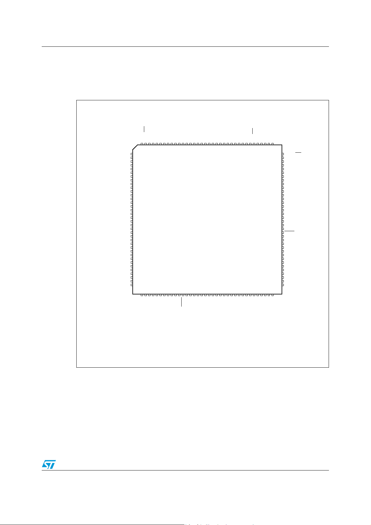
STR730F/STR735F
Note: CAN alternate functions not available on STR735F.
3.2 Pin description
3.2.1 STR730F/STR735F (TQFP144)
Figure 3. STR730F/STR735F pin configuration (top view)
11/52
Block diagram STR73xFxx
3.2.2 STR730F/STR735F (LFBGA144)
Table 3. STR730F/STR735F LFBGA ball connections
Ball Name Ball Name Ball Name Ball Name
A1 P0.0 / OCMPB2 B1 P0.4 / OCMPA5 C1 P0.5 / OCMPB5 D1 V
A2 P6.10 / WUP8 B2 P0.1 / OCMPA2 C2 P0.2 / ICAPA2 D2 V
A3 P6.9 / TDO0 B3 P6.15 / WUP9 C3 P0.3 / ICAPB2 D3 P0.6 / ICAPA5
A4 P6.12 / MOSI0 B4 P6.13 / SCKO / WUP11 C4 P6.14 / SSO D4 P0.7 /ICAPB5
A5 P6.6 / WUP6 B5 P6.7 / WUP7 C5 P6.8 / RDI0 / WUP10 D5 P6.11 / MISO0
A6 V
18
A7 P5.15 / INT13 B7 P5.14 / INT12 C7 V
B6 P6.2 / WUP2 / RDI3 C6 P6.3 / WUP3 D6 P6.4 / WUP4 /TDO3
SS
D7 VDD
A8 P5.8 / INT6 B8 P5.9 / INT7 C8 P5.10 / INT8 / RDI2 D8 P5.12 / INT10
A9 P5.2 / OCMPA9 B9 P5.3 / OCMPB9 C9 P5.4 / SS2 D9 P5.5 / SCK2 / WUP23
A10 P5.7 / MISO2 B10 P5.0 / MOSI1 C10 P5.1 / MISO1 D10 P4.13 / ICAPB9
A11 P5.6 / MOSI2 B11 P4.15 / SCK1 / WUP22 C11 P4.14 / SS1 D11 P4.12 / ICAPA9 / WUP21
A12 P5.11 / TDO2 / INT9 B12 P4.8 / OCMPA8 C12 P4.7 / SDA1 D12 P4.11 / OCMPB8
E1 P0.8 / OCMPA6 F1 V
DD
G1 V
SS
H1 V
E2 P0.9 / OCMPB6 F2 P0.13 / ICAPB3 G2 P1.2 / ICAPB4 H2 P1.8 / OCMPA0 / INT0
E3 P0.10 / OCMPA7 F3 P0.14 / OCMPB3 G3 P1.3 / ICAPA4 H3 P1.9 / OCMPB0 / INT1
E4 P0.11 / OCMPB7 F4 P0.15 / OCMPA3 G4 V
SS
H4 P1.10 / ICAPB0 / WUP28
E5 P0.12 / ICAPA3 F5 P1.0 / OCMPA4 G5 P1.5 H5 XTAL2
E6 P6.5 / WUP5 F6 P1.1 / OCMPB4 G6 P2.11 / WUP17 H6 P2.10 / WUP16
E7 P6.0 / WUP0 F7 P6.1 / WUP1 G7
E8 P5.13 / INT11 F8 P4.4 / CAN2TX
E9
P4.10 / ICAPA6 /
WUP20
F9
E10 P4.9 / ICAPB6 F10
E11 P4.6 / SCL1 / WUP19 F11
E12
P4.5 / WUP18 /
CAN2RX
1)
F12 JTDI G12 nJTRST H12 P3.14 / AIN14 / INT4
P4.3 / ICAPB8 /
WUP27
P4.2 / ICAPA8 /
WUP26
P4.1 / ICAPB7 /
WUP25
1)
G10 JTDO H10 VDD
G11 JTCK H11 P3.15 / AIN15 / INT5
G8 VDD H8 JTMS
G9 VSS H9 VSS
P4.0 / ICAPA7 /
WUP24
J1 P1.4 K1 P1.6 / OCMPB1 L1 P1.7 / OCMPA1 M1
J2
J3
P1.11 / ICAPA0 /
WUP29
P1.12 / ICAPA1 /
WUP30
K2
K3
P1.13 / ICAPB1 /
WUP31
P2.1 / CAN1RX
WUP13
L2 P1.15 / CAN0TX
1)
/
L3 P2.0 / PWM0 M3 P2.5 / PWM3
H7 P2.15 / SDA 0
P1.14 / CAN0RX
1)
M2 P2.4 / PWM2
J4 P2.7 / PWM5 K4 P2.6 / PWM4 L4 P2.3 / PWM1 M4 P2.2 / CAN1TX
J5 V
DD
J6 P2.9 / RDI1 / WUP14 K6 P2.8 / TDO1 L6 V
K5 M1 L5 RSTIN M5 M0
SS
M6 V
J7 P2.14 / SCL 0 / WUP15 K7 P2.13 / INT15 L7 P2.12 / INT14 M7 XTAL1
J8 P3.1 / AIN1 K8 P3.0 / AIN0 L8 VBIAS M8 TST
J9 P3.13 / AIN13 / INT3 K9 P3.4 / AIN4 L9 P3.3 / AIN3 M9 P3.2 / AIN2
J10 P3.12 / AIN12 / INT2 K10 V
J11 P3.9 / AIN9 K11 V
DDA
SSA
L10 P3.5 / AIN5 M10 V
L11 P3.7 / AIN7 M11 V
J12 P3.8 / AIN8 K12 P3.11 / AIN11 L12 P3.10 / AIN10 M12 P3.6 / AIN6
SS
DD
DD
WUP12
SS
SS
DD
1)
/
1)
Note: CAN alternate functions not available on STR735F.
12/52
STR73xFxx Block diagram
1
2
3
4
5
6
7
8
9
10
11
12
13
14
15
16
17
18
19
20
21
22
23
24
25
75
74
73
72
71
70
69
68
67
66
65
64
63
62
61
60
59
58
57
56
55
54
53
52
51
26272829303132333435363738394041424344454647484950
100999897969594939291908988878685848382818079787776
OCMPB2 / P0.0
OCMPA2 / P0.1
ICAPA2 / P0.2
ICAPB2 / P0.3
OCMPA5 / P0.4
OCMPB5 / P0.5
ICAPA5 / P0.6
V
DD
V
SS
ICAPA3 / P0.12
ICAPB3 / P0.13
OCMPB3 / P0.14
OCMPA3 / P0.15
OCMPA4 / P1.0
OCMPB4 / P1.1
ICAPB4 / P1.2
ICAPA4 / P1.3
OCMPB1 / P1.6
OCMPA1 / P1.7
INT0 / OCMPA0 / P1.8
INT1 / OCMPB0 / P1.9
ICAPB0 / WUP28 / P1.10
ICAPA0 / WUP29 / P1.11
ICAPA1 / WUP30 / P1.12
ICAPB1 / WUP31 / P1.13
P4.14 / SS1
P4.10 / ICAPB5 / WUP20
P4.7 / SDA1
P4.6 / SCL1 / WUP19
V
DD
V
SS
JTDO
JTCK
JTMS
JTDI
JTRST
V
SS
V
DD
P3.15 / AIN11 / INT5
P3.14 / AIN10 / INT4
P3.13 / AIN9 / INT3
P3.12 / AIN8 / INT2
P3.11 / AIN7
P3.10 / AIN6
P3.9 / AIN5
P3.8 / AIN4
V
DDA
V
SSA
P3.7 / AIN3
P3.6 / AIN2
WUP12 / CAN0RX / P1.14
CAN0TX / P1.15
PWM0 / P2.0
WUP13 / CAN1RX / P2.1
CAN1TX / P2.2
PWM1 / P2.3
PWM2 / P2.4
M0
RSTIN
M1
V
DD
V
SS
XTAL1
XTAL2
V
SS
CAN2RX / TDO1 / P2.8
WUP14 / CAN2TX / RDI1 / P2.9
WUP15 / SCL0 / P2.14
SDA0 / P2.15
TEST
V
BIAS
V
SS
V
DD
AIN0 / P3.4
AIN1 / P3.5
P6.14 / SS0
P6.13 / SCK0 / WUP11
P6.12 / MOSI0
P6.11 / MISO0
P6.9 / TDO0
P6.8 / RDI0 / WUP10
P6.6 / WUP6
P6.4 / TDO3 / WUP4
P6.2 / RDI3 / WUP2
P6.0 / WUP0
VDD
VSS
V18
P5.12 / INT10
P5.11 / TDO2 / INT9
P5.10 / RDI2 / INT8
P5.9 / PWM5 / INT7
P5.8 / PWM4 / INT6
P5.7 / MISO2
P5.6 / MOSI2
P5.5 / SCK2 / WUP23
P5.4 / SS2
/PWM3
P5.1 / MISO1
P5.0 / MOSI1
P4.15 / SCK1 / WUP22
STR731F/STR736F
Note: CAN alternate functions not available on STR736F.
3.2.3 STR731F/STR736F (TQFP100)
Figure 4. STR731F/STR736F pin configuration (top view)
13/52
Block diagram STR73xFxx
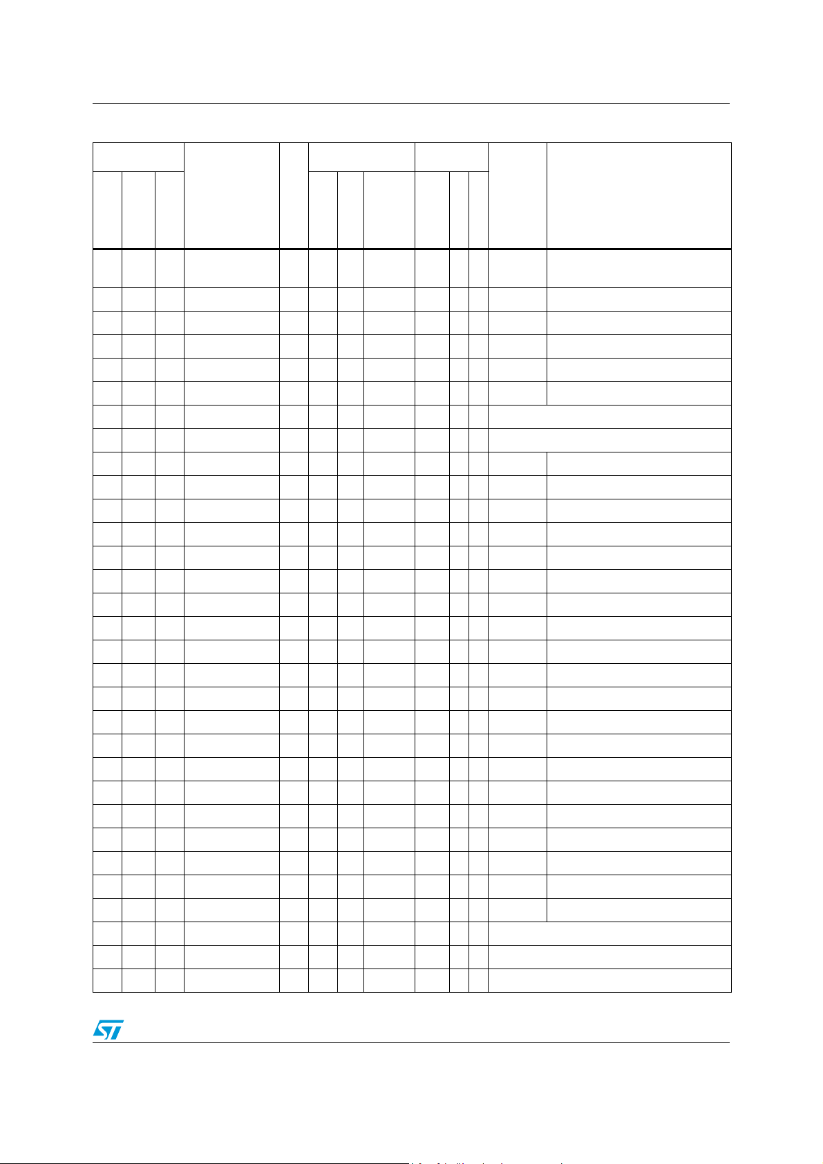
Legend / Abbreviations for Tab le 4 :
Type: I = input, O = output, S = supply, HiZ= high impedance,
In/Output level: T
= TTL 0.8 V / 2 V with input trigger
T
C
= CMOS 0.3VDD/0.7VDD with input trigger
T
Port and control configuration:
Input: pu/pd = with internal 100 kΩ weak pull-up or pull down
Output: OD = open drain
PP = push-pull
Interrupts:
INTx = external interrupt line
WUPx = wake-up interrupt line
The reset state (during and just after the reset) of the I/O ports is input floating (Input tristate
TTL mode). To avoid excess power consumption, unused I/O ports must be tied to ground.
LFBGA144
Pin name
TQFP100
SS
DD
P0.11/OCMPB
7
Type
T
T
T
T
S Ground
S Supply voltage (5 V)
T
T
T
T
T
T
T
I/O T
T
Table 4. STR73xF pin description
Pin n°
TQFP144
1 A1 1 P0.0/OCMPB2 I/O T
2B22P0.1/OCMPA2I/OT
3C23P0.2/ICAPA2 I/OT
4 C3 4 P0.3/ICAPB2 I/O T
5D1 V
6D2 V
7B15P0.4/OCMPA5I/OT
8 C1 6 P0.5/OCMPB5 I/O T
9D37P0.6/ICAPA5 I/OT
10 D4 P0.7/ICAPB5 I/O T
11 E1 P0.8/OCMPA6 I/O T
12 E2 P0.9/OCMPB6 I/O T
13 E3 P0.10/OCMPA7 I/O T
14 E4
(logic level)
Input Output
pu/pd
Input Level
interrupt
2mA X X Port 0.0 TIM2: output compare B output
2mA X X Port 0.1 TIM2: output compare A output
2mA X X Port 0.2 TIM2: input capture A input
2mA X X Port 0.3 TIM2: input capture B input
2mA X X Port 0.4 TIM5: output compare A output
2mA X X Port 0.5 TIM5: output compare B output
2mA X X Port 0.6 TIM5: input capture A input
2mA X X Port 0.7 TIM5: input capture B input
2mA X X Port 0.8 TIM6: output compare A output
2mA X X Port 0.9 TIM6: output compare B output
2mA X X Port 0.10 TIM7: output compare A output
2mA X X Port 0.11 TIM7: output compare B output
Main
OD
function
(after
PP
reset)
Alternate function
Capability
15 F1 8 V
16 G1 9 V
DD
SS
17 E5 10 P0.12/ICAPA3 I/O T
18 F2 11 P0.13/ICAPB3 I/O T
S Supply voltage (5 V)
S Ground
T
T
14/52
2mA X X Port 0.12 TIM3: input capture A input
2mA X X Port 0.13 TIM3: input capture B input
STR73xFxx Block diagram
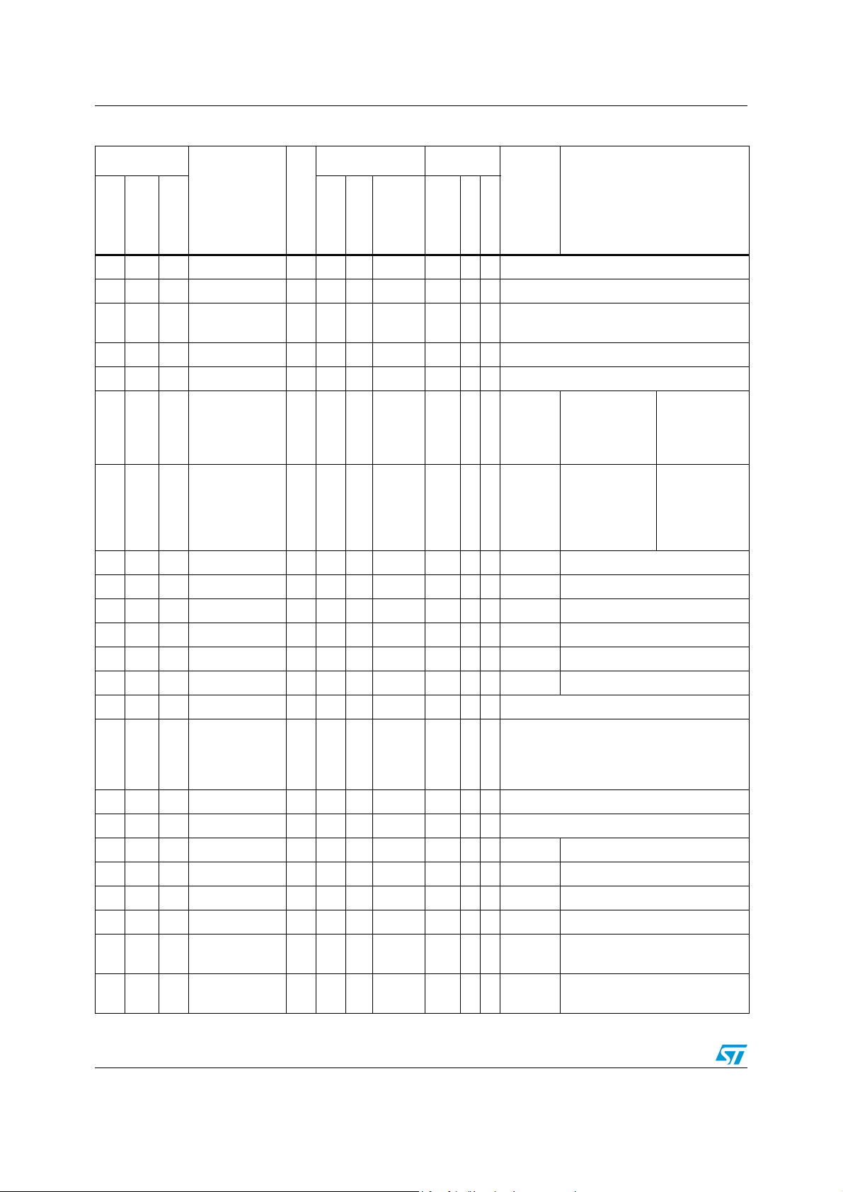
Table 4. STR73xF pin description
Pin n°
TQFP144
LFBGA144
19 F3 12
Pin name
TQFP100
P0.14/OCMPB
3
Typ e
I/O T
20 F4 13 P0.15/OCMPA3 I/O T
21 F5 14 P1.0/OCMPA4 I/O T
22 F6 15 P1.1/OCMPB4 I/O T
23 G2 16 P1.2/ICAPB4 I/O T
24 G3 17 P1.3/ICAPA4 I/O T
25 G4 V
26 H1 V
SS
DD
S Ground
S Supply voltage (5 V)
27 J1 P1.4 I/O T
28 G5 P1.5 I/O T
29 K1 18 P1.6/OCMPB1 I/O T
30 L1 19 P1.7/OCMPA1 I/O T
31 H2 20 P1.8/OCMPA0 I/O T
32 H3 21 P1.9/OCMPB0 I/O T
33 H4 22 P1.10/ICAPB0 I/O T
34 J2 23 P1.11/ICAPA0 I/O T
35 J3 24 P1.12/ICAPA1 I/O T
36 K2 25 P1.13/ICAPB1 I/O T
37 M1 26 P1.14/CAN0RX I/O T
38 L2 27 P1.15/CAN0TX I/O T
39 L3 28 P2.0/PWM0 I/O T
40 K3 29 P2.1/CAN1RX I/O T
41 M4 30 P2.2/CAN1TX I/O T
42 L4 31 P2.3/PWM1 I/O T
43 M2 32 P2.4/PWM2 I/O T
44 M3 P2.5/PWM3 I/O T
45 K4 P2.6/PWM4 I/O T
46 J4 P2.7/PWM5 I/O T
47 M5 33 M0 I T
48 L5 34 RSTIN I C
49 K5 35 M1 I T
Input Output
Main
function
(after
PP
OD
pu/pd
Input Level
T
T
T
T
T
T
T
T
T
T
T
T
T
T
T
T
T
T
T
T
T
T
T
T
T
T
pd BOOT: mode selection 0 input
T
pu Reset input
T
pd BOOT: mode selection 1 input
T
interrupt
INT0 2mA X X Port 1.8 TIM0: output compare A output
INT1 2mA X X Port 1.9 TIM0: output compare B output
WUP28 2mA X X Port 1.10 TIM0: input capture B input
WUP29 2mA X X Port 1.11 TIM0: input capture A input
WUP30 2mA X X Port 1.12 TIM1: input capture A input
WUP31 2mA X X Port 1.13 TIM1: input capture B input
WUP12 2mA X X Port 1.14 CAN0: receive data input
WUP13 2mA X X Port 2.1 CAN1: receive data input
Capability
2mA X X Port 0.14 TIM3: output compare B output
2mA X X Port 0.15 TIM3: output compare A output
2mA X X Port 1.0 TIM4: output compare A output
2mA X X Port 1.1 TIM4: output compare B output
2mA X X Port 1.2 TIM4: input capture B input
2mA X X Port 1.3 TIM4: input capture A input
2mA X X Port 1.4
2mA X X Port 1.5
2mA X X Port 1.6 TIM1: output compare B output
2mA X X Port 1.7 TIM1: output compare A output
2mA X X Port 1.15 CAN0: transmit data output
2mA X X Port 2.0 PWM0: PWM output
2mA X X Port 2.2 CAN1: transmit data output
2mA X X Port 2.3 PWM1: PWM output
2mA X X Port 2.4 PWM2: PWM output
2mA X X Port 2.5 PWM3: PWM output
2mA X X Port 2.6 PWM4: PWM output
2mA X X Port 2.7 PWM5: PWM output
reset)
Alternate function
15/52
Block diagram STR73xFxx
Table 4. STR73xF pin description
Pin n°
Input Output
Main
OD
function
(after
PP
reset)
Alternate function
Oscillator amplifier circuit input and
internal clock generator input.
Pin name
TQFP144
50 J5 36 V
51 M6 37 V
LFBGA144
TQFP100
DD
SS
52 M7 38 XTAL1 I
Typ e
pu/pd
Input Level
interrupt
Capability
S Supply voltage (5 V)
S Ground
53 H5 39 XTAL2 O Oscillator amplifier circuit output.
54 L6 40 V
55 K6 41
SS
P2.8/TDO1/CA
N2RX
S Ground
I/O T
T
2mA X X Port 2.8
UART1:
transmit data
output
CAN2: receive
data input
(TQFP100
only)
CAN2:
56 J6 42
P2.9/RDI1/CAN
2TX
I/O T
UART1:
T
WUP14 2mA X X Port 2.9
receive data
input
transmit data
output
(TQFP100
only)
57 H6 P2.10 I/O T
58 G6 P2.11 I/O T
59 L7 P2.12 I/O T
60 K7 P2.13 I/O T
61 J7 43 P2.14/SCL0 I/O T
62 H7 44 P2.15/SDA0 I/O T
T
T
T
T
T
T
WUP16 2mA X X Port 2.10
WUP17 2mA X X Port 2.11
INT14 2mA X X Port 2.12
INT15 2mA X X Port 2.13
WUP15 2mA X X Port 2.14 I2C0: serial clock
2mA X X Port 2.15 I2C0: serial data
63 M8 45 Test I pd Reserved pin. Must be tied to ground
64 L8 46 V
65 M10 47 V
66 M11 48 V
BIAS
SS
DD
67 K8 P3.0/AIN0 I/O T
68 J8 P3.1/AIN1 I/O T
69 M9 P3.2/AIN2 I/O T
70 L9 P3.3/AIN3 I/O T
71 K9 49 P3.4/AIN4 I/O T
72 L10 50 P3.5/AIN5 I/O T
S
S Ground
S Supply voltage (5 V)
T
T
T
T
T
T
16/52
Internal RC oscillator bias. A 1.3 MΩ
external resistor has to be connected to
this pin when a 32 kHZ RC oscillator
frequency is used.
2mA X X Port 3.0 ADC: analog input 0
2mA X X Port 3.1 ADC: analog input 1
2mA X X Port 3.2 ADC: analog input 2
2mA X X Port 3.3 ADC: analog input 3
2mA X X Port 3.4
2mA X X Port 3.5
ADC: analog input 4
(AIN0 in TQFP100)
ADC: Analog input 5
(AIN1 in TQFP100)
 Loading...