

ST STR710FZ1, STR710FZ2, STR711FR0, STR711FR1, STR711FR2 User Manual
...
ARM7TDMI™ 32-bit MCU with Flash, USB, CAN
5 timers, ADC, 10 communications interfaces
Features
■ Core
– ARM7TDMI 32-bit RISC CPU
– 59 MIPS @ 66 MHz from SRAM
– 45 MIPS @ 50 MHz from Flash
■ Memories
– Up to 256 Kbytes Flash program memory
(10 kcycles endurance, 20 years retention
@ 85° C)
– 16 Kbytes Flash data memory
(100 kcycles endurance, 20 years
retention@ 85° C)
– Up to 64 Kbytes RAM
– External Memory Interface (EMI) for up to 4
banks of SRAM, Flash, ROM
– Multi-boot capability
■ Clock, reset and supply management
– 3.0 to 3.6V application supply and I/Os
– Internal 1.8V regulator for core supply
– Clock input from 0 to 16.5 MHz
– Embedded RTC osc. running from external
32 kHz crystal
– Embedded PLL for CPU clock
– Realtime Clock for clock-calendar function
– 5 power saving modes: SLOW, WAIT,
LPWAIT, STOP and STANDBY modes
■ Nested interrupt controller
– Fast interrupt handling with multiple vectors
– 32 vectors with 16 IRQ priority levels
– 2 maskable FIQ sources
■ Up to 48 I/O ports
– 30/32/48 multifunctional bidirectional I/Os
Up to 14 ports with interrupt capability
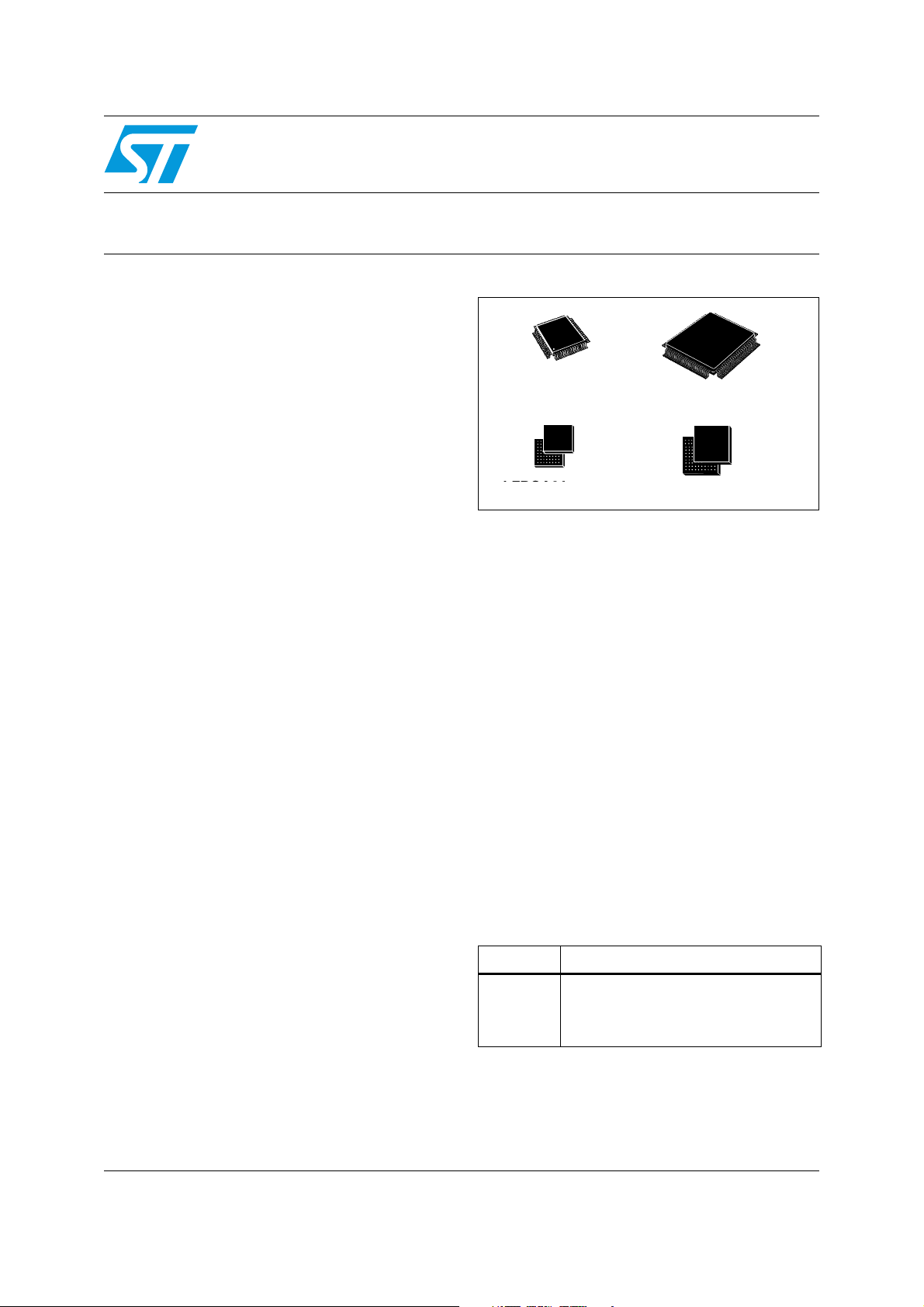
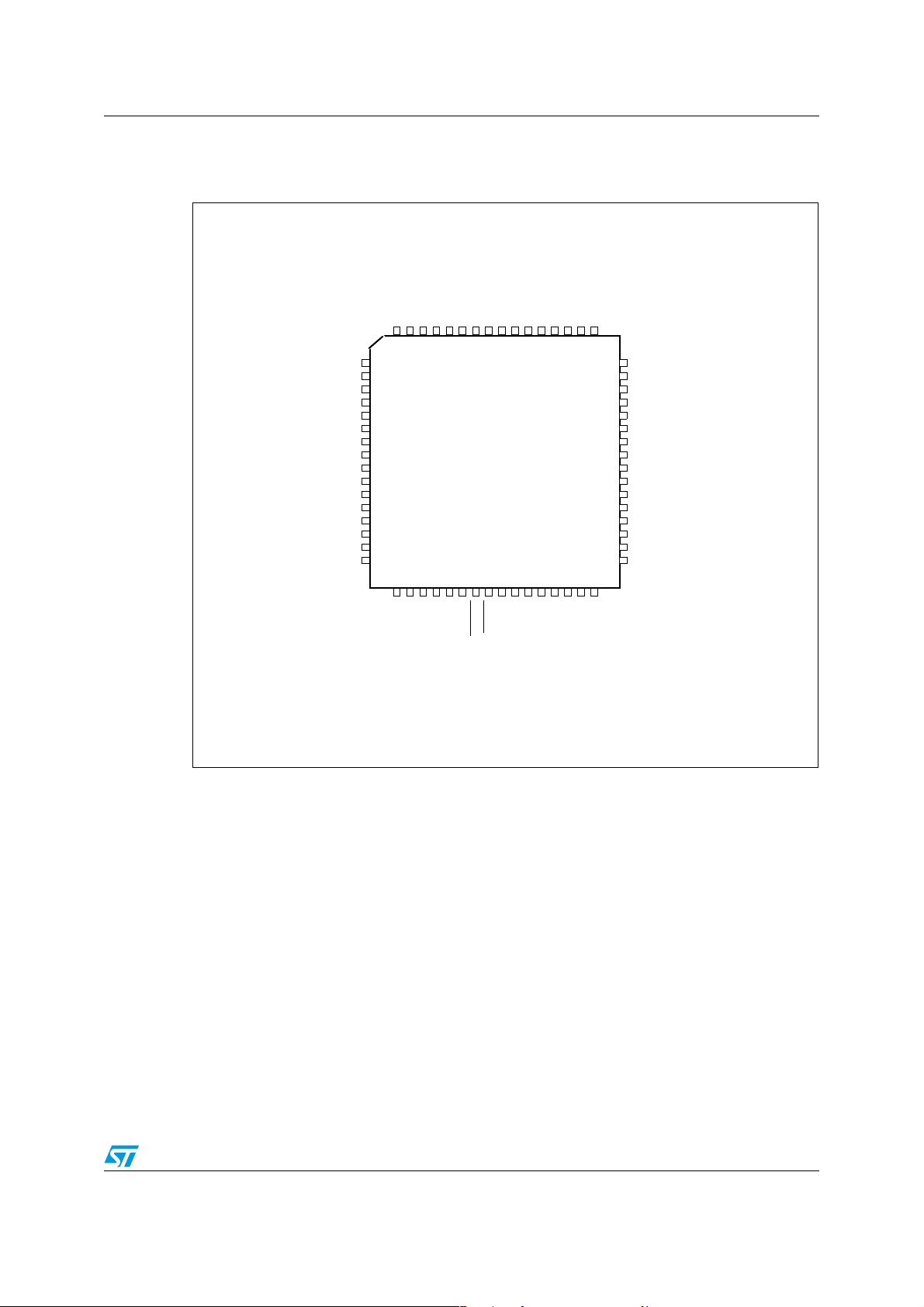
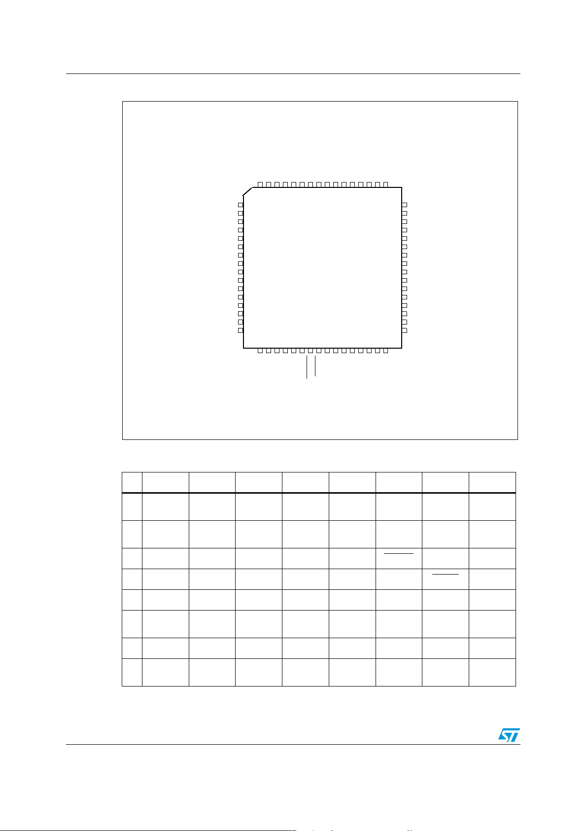
STR71xF
LQFP64
10 x 10
LFBGA64 8 x 8 x 1.7
LFBGA64 8 x 8 x 1.7
■ 5 Timers
– 16-bit watchdog timer
– 3 16-bit timers with 2 input captures, 2
output compares, PWM and pulse counter
– 16-bit timer for timebase functions
■ 10 communications interfaces
2
–2 I
C interfaces (1 multiplexed with SPI)
– 4 UART asynchronous serial interfaces
– Smartcard ISO7816-3 interface on UART1
– 2 BSPI synchronous serial interfaces
– CAN interface (2.0B Active)
– USB Full Speed (12 Mbit/s) Device
Function with Suspend and Resume
– HDLC synchronous communications
■ 4-channel 12-bit A/D converter
– Sampling frequency up to 1 kHz
– Conversion range: 0 to 2.5 V
■ Development tools support
– Atomic bit SET and RES operations
Table 1. Device summary
Reference Root part number
STR710FZ1, STR710FZ2,
STR71xF
STR711FR0, STR711FR1, STR711FR2,
STR712FR0, STR712FR1, STR712FR2,
STR715FR0
LQFP144
20 x 20
LFBGA144 10 x 10 x 1.7
February 2008 Rev 12 1/78
www.st.com
78

Contents STR71xF
Contents
1 Introduction . . . . . . . . . . . . . . . . . . . . . . . . . . . . . . . . . . . . . . . . . . . . . . . . 4
2 Description . . . . . . . . . . . . . . . . . . . . . . . . . . . . . . . . . . . . . . . . . . . . . . . . . 5
3 System architecture . . . . . . . . . . . . . . . . . . . . . . . . . . . . . . . . . . . . . . . . . 6
3.1 On-chip peripherals . . . . . . . . . . . . . . . . . . . . . . . . . . . . . . . . . . . . . . . . . . 7
3.2 Related documentation . . . . . . . . . . . . . . . . . . . . . . . . . . . . . . . . . . . . . . 10
3.3 Pin description for 144-pin packages . . . . . . . . . . . . . . . . . . . . . . . . . . . . 11
3.4 Pin description for 64-pin packages . . . . . . . . . . . . . . . . . . . . . . . . . . . . . 21
3.5 External connections . . . . . . . . . . . . . . . . . . . . . . . . . . . . . . . . . . . . . . . . 28
3.6 I/O port configuration . . . . . . . . . . . . . . . . . . . . . . . . . . . . . . . . . . . . . . . . 29
3.7 Memory mapping . . . . . . . . . . . . . . . . . . . . . . . . . . . . . . . . . . . . . . . . . . . 30
4 Electrical parameters . . . . . . . . . . . . . . . . . . . . . . . . . . . . . . . . . . . . . . . 33
4.1 Parameter conditions . . . . . . . . . . . . . . . . . . . . . . . . . . . . . . . . . . . . . . . . 33
4.1.1 Minimum and maximum values . . . . . . . . . . . . . . . . . . . . . . . . . . . . . . . 33
4.1.2 Typical values . . . . . . . . . . . . . . . . . . . . . . . . . . . . . . . . . . . . . . . . . . . . . 33
4.1.3 Typical curves . . . . . . . . . . . . . . . . . . . . . . . . . . . . . . . . . . . . . . . . . . . . 33
4.1.4 Loading capacitor . . . . . . . . . . . . . . . . . . . . . . . . . . . . . . . . . . . . . . . . . 33
4.1.5 Pin input voltage . . . . . . . . . . . . . . . . . . . . . . . . . . . . . . . . . . . . . . . . . . 33
4.2 Absolute maximum ratings . . . . . . . . . . . . . . . . . . . . . . . . . . . . . . . . . . . . 34
4.3 Operating conditions . . . . . . . . . . . . . . . . . . . . . . . . . . . . . . . . . . . . . . . . 36
4.3.1 Supply current characteristics . . . . . . . . . . . . . . . . . . . . . . . . . . . . . . . . 37
4.3.2 Clock and timing characteristics . . . . . . . . . . . . . . . . . . . . . . . . . . . . . . 41
4.3.3 Memory characteristics . . . . . . . . . . . . . . . . . . . . . . . . . . . . . . . . . . . . . 46
4.3.4 EMC characteristics . . . . . . . . . . . . . . . . . . . . . . . . . . . . . . . . . . . . . . . . 47
4.3.5 I/O port pin characteristics . . . . . . . . . . . . . . . . . . . . . . . . . . . . . . . . . . . 50
4.3.6 TIM timer characteristics . . . . . . . . . . . . . . . . . . . . . . . . . . . . . . . . . . . . 56
4.3.7 EMI - external memory interface . . . . . . . . . . . . . . . . . . . . . . . . . . . . . . 56
4.3.8 I2C - inter IC control interface . . . . . . . . . . . . . . . . . . . . . . . . . . . . . . . . 60
4.3.9 BSPI - buffered serial peripheral interface . . . . . . . . . . . . . . . . . . . . . . . 63
4.3.10 USB characteristics . . . . . . . . . . . . . . . . . . . . . . . . . . . . . . . . . . . . . . . . 65
4.3.11 ADC characteristics . . . . . . . . . . . . . . . . . . . . . . . . . . . . . . . . . . . . . . . . 66
2/78

STR71xF Contents
5 Package characteristics . . . . . . . . . . . . . . . . . . . . . . . . . . . . . . . . . . . . . 69
5.1 Package mechanical data . . . . . . . . . . . . . . . . . . . . . . . . . . . . . . . . . . . . 69
5.2 Thermal characteristics . . . . . . . . . . . . . . . . . . . . . . . . . . . . . . . . . . . . . . 72
6 Product history . . . . . . . . . . . . . . . . . . . . . . . . . . . . . . . . . . . . . . . . . . . . 73
7 Ordering information . . . . . . . . . . . . . . . . . . . . . . . . . . . . . . . . . . . . . . . 75
8 Revision history . . . . . . . . . . . . . . . . . . . . . . . . . . . . . . . . . . . . . . . . . . . 76
Note: For detailed information on the STR71x Microcontroller memory, registers and peripherals,
please refer to the STR71x Reference Manual.
3/78
Introduction STR71xF
1 Introduction
This datasheet provides the STR71x pinout, ordering information, mechanical and electrical
device characteristics.
For complete information on the STR71x microcontroller memory, registers and peripherals.
please refer to the STR71x reference manual.
For information on programming, erasing and protection of the internal Flash memory
please refer to the STR7 Flash programming reference manual.
For information on the ARM7TDMI core please refer to the ARM7TDMI technical reference
manual.
Table 2. Device overview
Features
Flash - Kbytes 128+16 256+16 0 64+16 128+16 256+16 64+16 128+16 256+16 64+16
RAM - Kbytes 32 64 64 16 32 64 16 32 64 16
Peripheral
Functions
Operating
Voltage
Operating
Temperature
Packages
STR710
FZ1
STR710
FZ2
STR710RZSTR711
FR0
STR711
FR1
STR711
FR2
STR712
FR0
STR712
FR1
STR712
FR2
CAN, EMI, USB, 48 I/Os USB, 30 I/Os CAN, 32 I/Os 32 I/Os
3.0 to 3.6 V
-40 to +85°C or 0 to 70° C
T=LQFP144 20 x 20
H=LFBGA144 10 x10
T=LQFP64 10 x10 / H=LFBGA64 8 x 8 x 1.7
STR715
FRx
.
4/78

STR71xF Description
2 Description
ARM® core with embedded Flash and RAM
The STR71x series is a family of ARM-powered 32-bit microcontrollers with embedded
Flash and RAM. It combines the high performance ARM7TDMI CPU with an extensive
range of peripheral functions and enhanced I/O capabilities. STR71xF devices have on-chip
high-speed single voltage FLASH memory and high-speed RAM. STR710R devices have
high-speed RAM but no internal Flash. The STR71x family has an embedded ARM core and
is therefore compatible with all ARM tools and software.
Extensive tools support
STMicroelectronics’ 32-bit, ARM core-based microcontrollers are supported by a complete
range of high-end and low-cost development tools to meet the needs of application
developers. This extensive line of hardware/software tools includes starter kits and complete
development packages all tailored for ST’s ARM core-based MCUs. The range of
development packages includes third-party solutions that come complete with a graphical
development environment and an in-circuit emulator/programmer featuring a JTAG
application interface. These support a range of embedded operating systems (OS), while
several royalty-free OSs are also available.
For more information, please refer to ST MCU site http://www.st.com/mcu
5/78

System architecture STR71xF
3 System architecture
Package choice: low pin-count 64-pin or feature-rich 144-pin LQFP or BGA
The STR71x family is available in 5 main versions.
The 144-pin versions have the full set of all features including CAN, USB and External
Memory Interface (EMI).
● STR710F: 144-pin BGA or LQFP with CAN, USB and EMI
● STR710R: Flashless 144-pin BGA or LQFP with CAN, USB and EMI (no internal Flash
memory)
The three 64-pin versions (BGA or LQFP) do not include External Memory Interface.
● STR715F: 64-pin BGA or LQFP without CAN or USB
● STR711F: 64-pin BGA or LQFP with USB
● STR712F: 64-pin BGA or LQFP with CAN
High speed Flash memory (STR71xF)
The Flash program memory is organized in two banks of 32-bit wide Burst Flash memories
enabling true read-while-write (RWW) operation. Device Bank 0 is up to 256 Kbytes in size,
typically for the application program code. Bank 1 is 16 Kbytes, typically used for storing
data constants. Both banks are accessed by the CPU with zero wait states @ 33 MHz
Bank 0 memory endurance is 10K write/erase cycles and Bank 1 endurance is 100K
write/erase cycles. Data retention is 20 years at 85°C on both banks. The two banks can be
accessed independently in read or write. Flash memory can be accessed in two modes:
● Burst mode: 64-bit wide memory access at up to 50 MHz.
● Direct 32-bit wide memory access for deterministic operation at up to 33 MHz.
The STR7 embedded Flash memory can be programmed using In-Circuit Programming or
In-Application programming.
IAP (in-application programming): The IAP is the ability to re-program the Flash memory
of a microcontroller while the user program is running.
ICP (in-circuit programming): The ICP is the ability to program the Flash memory of a
microcontroller using JTAG protocol while the device is mounted on the user application
board.
The Flash memory can be protected against different types of unwanted access
(read/write/erase). There are two types of protection:
● Sector Write Protection
● Flash Debug Protection (locks JTAG access)
Refer to the STR7 Flash Programming Reference manual for details.
Optional external memory (STR710)
The non-multiplexed 16-bit data/24-bit address bus available on the STR710 (144-pin)
supports four 16-Mbyte banks of external memory. Wait states are programmable
individually for each bank allowing different memory types (Flash, EPROM, ROM, SRAM
etc.) to be used to store programs or data.
Figure 1 shows the general block diagram of the device family.
6/78

STR71xF System architecture
Flexible power management
To minimize power consumption, you can program the STR71x to switch to SLOW, WAIT,
LPWAIT (low power wait), STOP or STANDBY mode depending on the current system
activity in the application.
Flexible clock control
Two external clock sources can be used, a main clock and a 32 kHz backup clock. The
embedded PLL allows the internal system clock (up to 66 MHz) to be generated from a main
clock frequency of 16 MHz or less. The PLL output frequency can be programmed using a
wide selection of multipliers and dividers. The microcontroller core, APB1 and APB2
peripherals are in separate clock domains and can be programmed to run at different
frequencies during application runtime. The clock to each peripheral is gated with an
individual control bit to optimize power usage by turning off peripherals any time they are not
required.
Voltage regulators
The STR71x requires an external 3.0-3.6V power supply. There are two internal Voltage
Regulators for generating the 1.8V power supply for the core and peripherals. The main VR
is switched off during low power operation.
Low voltage detectors
Both the Main Voltage Regulator and the Low Power Voltage Regulator contain each a low
voltage detection circuitry which keep the device under reset when the corresponding
controlled voltage value (V
18
or V
) falls below 1.35V (+/- 10%). This enhances the
18BKP
security of the system by preventing the MCU from going into an unpredictable state.
An external reset circuit must be used to provide the RESET at V
sufficient to rely on the RESET generated by the LVD in this case. This is because LVD
operation is guaranteed only when V
3.1 On-chip peripherals
CAN interface (STR710 and STR712)
The CAN module is compliant with the CAN specification V2.0 part B (active). The bit rate
can be programmed up to 1 MBaud.
USB interface (STR710 and STR711)
The full-speed USB interface is USB V2.0 compliant and provides up to 16 bidirectional/32
unidirectional endpoints, up to 12 Mb/s (full-speed), support for bulk transfer, isochronous
transfers and USB Suspend/Resume functions.
Standard timers
Each of the four timers have a 16-bit free-running counter with 7-bit prescaler
Three timers each provide up to two input capture/output compare functions, a pulse
counter function, and a PWM channel with selectable frequency.
The fourth timer is not connected to the I/O ports. It can be used by the application software
for general timing functions.
is within the specification.
33
power-up. It is not
33
7/78

System architecture STR71xF
Realtime clock (RTC)
The RTC provides a set of continuously running counters driven by the 32 kHz external
crystal. The RTC can be used as a general timebase or clock/calendar/alarm function.
When the STR71x is in Standby mode the RTC can be kept running, powered by the low
power voltage regulator and driven by the 32 kHz external crystal.
UARTs
The 4 UARTs allow full duplex, asynchronous, communications with external devices with
independently programmable TX and RX baud rates up to 1.25 Mb/s.
Smartcard interface
UART1 is configurable to function either as a general purpose UART or as an asynchronous
Smartcard interface as defined by ISO 7816-3. It includes Smartcard clock generation and
provides support features for synchronous cards.
Buffered serial peripheral interfaces (BSPI)
Each of the two SPIs allow full duplex, synchronous communications with external devices,
master or slave communication at up to 5.5 Mb/s in Master mode and 4 Mb/s in Slave mode.
2
I
C interfaces
The two I
2
I
C mode (400 kHz) and 7 or 10-bit addressing modes.
One I
2
C Interfaces provide multi-master and slave functions, support normal and fast
2
C Interface is multiplexed with one SPI, so either 2xSPI+1x I2C or 1xSPI+2x I2C may
be used at a time.
HDLC interface
The High Level Data Link Controller (HDLC) unit supports full duplex operation and NRZ,
NRZI, FM0 or MANCHESTER protocols. It has an internal 8-bit baud rate generator.
A/D converter
The Analog to Digital Converter, converts in single channel or up to 4 channels in singleshot or round robin mode. Resolution is 12-bit with a sampling frequency of up to 1 kHz. The
input voltage range is 0-2.5V.
Watchdog
The 16-bit Watchdog Timer protects the application against hardware or software failures
and ensures recovery by generating a reset.
I/O ports
The 48 I/O ports are programmable as Inputs or Outputs.
External interrupts
Up to 14 external interrupts are available for application use or to wake up the application
from STOP mode.
8/78
STR71xF System architecture
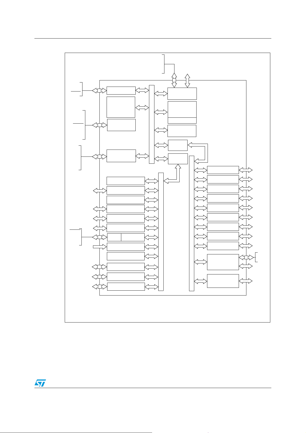
Figure 1. STR71x block diagram
A[19:0]
D[15:0]
CK
CKOUT
RSTIN
RDN
WEN[1:0]
PRCCU/PLL
A[23:20] (AF)
CS[3:0)
EXT. MEM.
INTERFACE (EMI)
JTDI
JTCK
JTMS
JTRST
JTDO
DBGRQS
BOOTEN
V18[1:0]
V33[6:0]
VSS[9:0]
V18BKP
AVDD
AVSS
STDBY
RTCXTO
RTCXTI
WAKEUP
4 AF
4 AF
2 AF
4 AF
14 AF
P0[15:0]
ARM7TDMI
CPU
JTAG
POWER SUPPLY
VREG
INTERRUPT CTL(EIC)
A/D
TIMER0
TIMER1
TIMER2
TIMER3
OSC
RTC
EXT INT (XTI)
WATCHDOG
I/O PORT 0
FLASH*
Program Memory
64/128/256K
16K Data FLASH*
RAM
APB BUS
16/32/64K
APB
BRIDGE 1
APB
BRIDGE 2
I2C0
I2C1
BSPI0
BSPI1
UART0
UART1 /
APB BUS
SMARTCARD
UART2
UART3
HDLC
USB
2 AF
2 AF
4 AF
4 AF
2 AF
3 AF
2 AF
2 AF
3 AF
USBDP
USBDN
1 AF
ARM7 NATIVE BUS
P1[15:0]
P2[15:0]
*Flash present in STR710F, not in STR710R
I/O PORT 1
I/O PORT 2
CAN
AF: alternate function on I/O port pin
2 AF
9/78

System architecture STR71xF
3.2 Related documentation
Available from www.arm.com:
ARM7TDMI Technical reference manual
Available from http://www.st.com:
STR71x Reference manual
STR7 Flash programming manual
AN1774 - STR71x Software development getting started
AN1775 - STR71x Hardware development getting started
AN1776 - STR71x Enhanced interrupt controller
AN1777 - STR71x memory mapping
AN1780 - Real time clock with STR71x
AN1781 - Four 7 segment display drive using the STR71x
The above is a selected list only, a full list STR71x application notes can be viewed at
http://www.st.com.
10/78
STR71xF System architecture
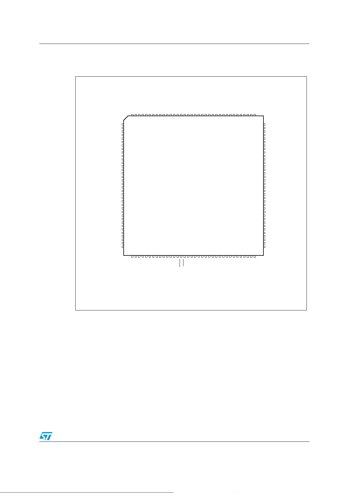
3.3 Pin description for 144-pin packages
Figure 2. STR710 LQFP pinout
P0.9/U0.TX/BOOT.0
P0.8/U0.RX/U0.TX
P0.7/S1.SSN
P0.6/S1.SCLK
P0.5/S1.MOSI
VSS
V33
WEn.0
WEn.1
A.19
A.18
A.17
A.16
A.15
A.14
V18
VSS18
P0.4/S1.MISO
P0.3/S0.SSN/I1.SDA
P0.2/S0.SCLK/I1.SCL
P0.1/S0.MOSI/U3.RX
P0.0/S0.MISO/U3.TX
A.13
A.12
A.11
A.10
A.9
A.8
A.7
A.6
A.5
V33
VSS
P1.15/HTXD
N.C.
N.C.
144
143
142
141
140
139
138
137
136
135
134
133
132
131
130
129
128
127
126
125
124
123
122
121
120
119
118
117
116
115
114
113
112
111
110
P0.10/U1.RX/U1.TX/SC DATA
P0.11/U1.TX/BOOT.1
P0.12/SCCLK
P2.0/CSn.0
P2.1/CSn.1
P0.13/U2.RX/T2.OCMPA
P0.14/U2.TX/T2.ICAPA
P2.2/CSn.2
P2.3/CSn.3
P2.4/A.20
P2.5/A.21
P2.6/A.22
BOOTEN
P2.7/A.23
P2.10
P2.11
P2.12
P2.13
P2.14
P2.15
JTMS
JTCK
JTDO
JTRSTn
TEST
1
2
RDn
3
4
5
VSS
6
V33
7
8
9
10
11
12
13
14
15
16
17
18
P2.8
19
N.C.
20
N.C.
21
VSS
22
V33
23
P2.9
24
25
26
27
28
29
30
JTDI
31
32
33
34
35
NU
36
3738394041424344454647484950515253545556575859606162636465666768697071
N.C.
N.C.
TEST
V33IO-PLL
CK
N.C.
N.C.
CKOUT
DBGRQS
VSSIO-PLL
N.C.
P0.15/WAKEUP
LQFP144
RSTIN
STDBY
RTCXTI
RTCXTO
V18
N.C.
N.C.
N.C.
N.C.
VSS18
V18BKP
VSSBKP
D.0
D.1
D.2
D.3
D.4
AVSS
AVDD
109
108
P1.14/HRXD/I0.SDA
107
P1.13/HCLK/I0.SCL
106
P1.10/USBCLK
105
P1.9
104
V33
103
VSS
102
A.4
101
A.3
100
A.2
99
A.1
98
A.0
97
D.15
96
D.14
95
D.13
94
D.12
93
D.11
92
D.10
91
USBDN
90
USBDP
89
P1.12/CANTX
88
P1.11/CANRX
87
N.C.
86
P1.8
85
P1.7/T1.OCMPA
84
VSSIO-PLL
83
V33IO-PLL
82
D.9
81
D.8
80
D.7
79
D.6
78
D.5
77
P1.6/T1.OCMPB
76
P1.5/T1.ICAPB
75
P1.4/T1.ICAPA
74
P1.3/T3.ICAPB/AIN.3
73
P1.2/T3.OCMPA/AIN.2
72
N.C.
N.C.
N.C.
P1.1/T3.ICAPA/AIN.1
P1.0/T3.OCMPB/AIN.0
11/78

System architecture STR71xF
Table 3. STR710 BGA ball connections
ABCDEFGHJ K LM
1 P0.10 P2.0 P2.1 VSS P2.2 P2.6
2 VSS RDn P0.11 V33 P2.3 P2.8 P2.9 JTMS
3 V33 P0.9 P0.12 P0.13 P2.4 N.C. P2.10 JTCK NU V33 N.C.
4 P0.6 P0.7 P0.8 P0.14 P2.5 N.C. P2.11 JTDO CK CKOUT
5 A.19 WEn.1 WEn.0 P0.5 P2.7 VSS P2.14 N.C.
6 P0.3 A.15 A.16 A.17 A.18 V33 V18 N.C. N.C.
7 P0.2 P0.1 P0.4 VSS18 V18 A.14 D.12 D.1 D.0 nc VSS18 RSTIN
8 A.9 A.10 A.11 A.13 P0.0 A.0 D.11
9 VSS V33 A.5 A.6 V33 D.15 D.10 P1.8 D.9 P1.0 N.C. N.C.
10 A.8 N.C. P1.15 P1.13 VSS D.14 USBDN P1.7 D.8 P1.5 P1.1 D.4
11 A.7 N.C. P1.14 P1.10 A.2 D.13 USBDP VSS D.5 P1.4 P1.3 AVDD
12 A.12 A.4 A.3 P1.9 A.1
P1.11/
CANRX
BOOT
EN
N.C.
P2.12 P2.13 P2.15 JTDI N.C.
JTRST
RTCX-
P1.12/
CANTX
V33IO-
PLL
TEST TEST N.C.
n
DBG
RQS
VSSIO-
PLL
RTCXTI N.C. P0.15
TO
V18BKPVSS
N.C. AVSS D.3 D.2
P1.6 D.7 D.6 P1.2
BKP
N.C.
STDBY
Legend / abbreviations for Ta bl e 4 :
Type: I = input, O = output, S = supply, HiZ= high impedance,
In/Output level: C = CMOS 0.3V
DD
/0.7V
DD
CT= CMOS 0.3VDD/0.7VDD with input trigger
T
= TTL 0.8 V/2 V with input trigger
T
C/T = Programmable levels: CMOS 0.3V
/0.7VDD or TTL 0.8 V / 2 V
DD
Port and control configuration:
Input: pu/pd= software enabled internal pull-up or pull down
pu= in reset state, the internal 100kΩ weak pull-up is enabled.
pd = in reset state, the internal 100kΩ weak pull-down is enabled.
Output: OD = open drain
(logic level)
PP = push-pull
T = true OD, (P-Buffer and protection diode to V
not implemented),
DD
5 V tolerant.
12/78

STR71xF System architecture
BGA144
Pin name
Typ e
Input Output
1)
Reset state
Table 4. STR710 pin description
Pin n°
LQFP144
P0.10/U1.RX/
1A1
U1.TX/
I/O pd CTX 4mA T Port 0.10
SC.DATA
5)
2B2RD
3C2
P0.11/BOOT.1
/U1.TX
O
I/O pd C
T
PP
OD
interrupt
Input level
Capability
X
4mA X X Port 0.11
Main
function
(after
Alternate function
reset)
Active in Stdby
UART1:
Receive Data
input
UART1: Transmit
data output.
Note: This pin may be used for
Smartcard DataIn/DataOut or single
wire UART (half duplex) if
programmed as Alternate Function
Output. The pin will be tri-stated
except when UART transmission is in
progress
External Memory Interface: Active low read signal
for external memory. It maps to the OE_N input of
the external components.
Select Boot
Configuration
input
UART1: Transmit
data output.
4 C3 P0.12/SC.CLK I/O pd C
5D1V
6D2V
SS
33
7 B1 P2.0/CS.0 I/O
8 C1 P2.1/CS
9D3
10 D4
P0.13/U2.RX/
T2.OCMPA
P0.14/U2.TX/
T2.ICAPA
.1 I/O
11 E1 P2.2/CS.2 I/O
12 E2 P2.3/CS
.3 I/O
S Ground voltage for digital I/Os
S Supply voltage for digital I/Os
8)
pu
2)
I/O pu C
I/O pu C
pu
2)
pu
2)
4mA X X Port 0.12 Smartcard reference clock output
T
C
C
C
C
8mA X X Port 2.0
T
8mA X X Port 2.1
T
X 4mA X X Port 0.13
T
4mA X X Port 0.14
T
8mA X X Port 2.2
T
8mA X X Port 2.3
T
4)
4)
External Memory Interface: Select
Memory Bank 0 output
Note: This pin is forced to output
push-pull 1 mode at reset to allow
boot from external memory
External Memory Interface: Select
Memory Bank 1 output
UART2:
Receive Data
input
UART2:
Transmit data
output
Timer2: Output
Compare A output
Timer2: Input
Capture A input
External Memory Interface: Select
Memory Bank 2 output
External Memory Interface: Select
Memory Bank 3 output
13/78
System architecture STR71xF
Table 4. STR710 pin description
Pin n°
LQFP144
Pin name
BGA144
Typ e
13 E3 P2.4/A.20 I/O
14 E4 P2.5/A.21 I/O
15 F1 P2.6/A.22 I/O
16 G1 BOOTEN I C
17 E5 P2.7/A.23 I/O
18 F2 P2.8 I/O pu C
Input Output
1)
Reset state
Input level
pd
C
3)
T
pd
C
3)
T
pd
C
3)
T
T
pd
C
3)
T
X 4mA X X Port 2.8 External interrupt INT2
T
Main
function
(after
PP
interrupt
OD
Capability
reset)
Active in Stdby
8mA X X Port 2.4
8mA X X Port 2.5
8mA X X Port 2.6
Boot control input. Enables sampling of
BOOT[1:0] pins
8mA X X Port 2.7
Alternate function
External Memory Interface: address
bus
External Memory Interface: address
bus
19 F3 N.C. Not connected (not bonded)
20 F4 N.C. Not connected (not bonded)
21 F5 V
22 F6 V
SS
33
23 G2 P2.9 I/O pu C
24 G3 P2.10 I/O pu C
25 G4 P2.11 I/O pu C
26 H1 P2.12 I/O pu C
27 J1 P2.13 I/O pu C
28 G5 P2.14 I/O pu C
29 K1 P2.15 I/O pu C
30 L1 JTDI I T
31 H2 JTMS I T
32 H3 JTCK I C
S Ground voltage for digital I/Os4)
S Supply voltage for digital I/Os4)
X 4mA X X Port 2.9 External interrupt INT3
T
X 4mA X X Port 2.10 External interrupt INT4
T
X 4mA X X Port 2.11 External interrupt INT5
T
4mA X X Port 2.12
T
4mA X X Port 2.13
T
4mA X X Port 2.14
T
4mA X X Port 2.15
T
T
T
JTAG Data input. External pull-up required.
JTAG Mode Selection Input. External pull-up
required.
JTAG Clock Input. External pull-up or pull-down
required.
33 H4 JTDO O 8mA X JTAG Data output. Note: Reset state = HiZ.
34 J2 JTRST I T
T
JTAG Reset Input. External pull-up required.
35 J3 NU Reserved, must be forced to ground.
36 K2 TEST Reserved, must be forced to ground.
37 M1 N.C. Not connected (not bonded)
38 L2 TEST Reserved, must be forced to ground.
39 L3 N.C. Not connected (not bonded)
14/78
STR71xF System architecture
Table 4. STR710 pin description
Pin n°
BGA144
LQFP144
40 K3 V
Pin name
33IO-PLL
Typ e
S
Input Output
1)
Reset state
interrupt
Input level
Main
function
(after
PP
OD
Capability
reset)
Active in Stdby
Alternate function
Supply voltage for digital I/O circuitry and for PLL
reference
41 M4 N.C. Not connected (not bonded)
42 L4 V
SSIO-PLL
S
Ground voltage for digital I/O circuitry and for PLL
reference
4)
43 M2 N.C. Not connected (not bonded)
44 M3 DBGRQS I C
T
45 K4 CKOUT O 8mA X
Debug Mode request input (active high)
Clock output (f
) Note: Enabled by CKDIS
PCLK2
register in APB Bridge 2
46 J4 CK I C Reference clock input
47 M5
P0.15/
WAKEU P
IT
XX
T
Port 0.15 Wakeup from Standby mode input.
Note: This port is input only.
48 L5 N.C. Not connected (not bonded)
49 K5 RTCXTI
Realtime Clock input and input of 32 kHz
oscillator amplifier circuit
50 J5 RTCXTO Output of 32 kHz oscillator amplifier circuit
Input: Hardware Standby mode entry input active
low. Caution: External pull-up to V
required to
33
select normal mode.
51 M6 STDBY
I/O C
4mA X X
T
Output: Standby mode active low output following
Software Standby mode entry.
Note: In Standby mode all pins are in high
impedance except those marked Active in Stdby
52 M7 RSTIN
IC
T
X Reset input
53 H5 N.C. Not connected (not bonded)
54 L6 V
SSBKP
S X Stabilization for low power voltage regulator.
Stabilization for low power voltage regulator.
Requires external capacitors of at least 1µF
55 K6 V
18BKP
SX
between V
Note: If the low power voltage regulator is
18BKP
and V
SS18BKP
. See Figure 5.
bypassed, this pin can be connected to an
external 1.8V supply.
56 J6 N.C. Not connected (not bonded)
57 H6 N.C. Not connected (not bonded)
Stabilization for main voltage regulator. Requires
58 G6 V
18
S
external capacitors of at least 10µF + 33nF
between V
and V
18
. See Figure 5.
SS18
15/78

System architecture STR71xF
Table 4. STR710 pin description
Pin n°
BGA144
LQFP144
59 L7 V
Pin name
SS18
Typ e
S Stabilization for main voltage regulator.
Input Output
1)
Reset state
interrupt
Input level
Main
function
(after
PP
OD
Capability
reset)
Active in Stdby
Alternate function
60 K7 N.C. Not connected (not bonded)
61 J7 D.0 I/O
62 H7 D.1 I/O
63 M8 D.2 I/O
64 L8 D.3 I/O
65 M10 D.4 I/O
66 M11 V
67 K8 V
DDA
SSA
S Supply voltage for A/D Converter
S Ground voltage for A/D Converter
6)
6)
6)
6)
6)
8mA
8mA
8mA
8mA
8mA
External Memory Interface: data bus
68 J8 N.C. Not connected (not bonded)
69 M9 N.C. Not connected (not bonded)
70 L9 N.C. Not connected (not bonded)
Timer 3:
Output
Compare B
Timer 3: Input
Capture A or
External Clock
input
Timer 3:
Output
Compare A
Timer 3: Input
Capture B
Timer 1: Input
Capture A
71 K9
72 L10
73 M12
74 L11
75 K11
P1.0/T3.OCM
PB/AIN.0
P1.1/T3.ICAP
A/T3.EXTCLK/
AIN.1
P1.2/T3.OCM
PA/AIN.2
P1.3/T3.ICAP
B/AIN.3
P1.4/T1.ICAP
A/T1.EXTCLK
I/O pu C
I/O pu C
I/O pu C
I/O pu C
I/O pu C
4mA X X Port 1.0
T
4mA X X Port 1.1
T
4mA X X Port 1.2
T
4mA X X Port 1.3
T
4mA X X Port 1.4
T
ADC: Analog input 0
ADC: Analog input 1
ADC: Analog input 2
ADC: Analog input 3
Timer 1: External
Clock input
76 K10
77 J12
P1.5/T1.ICAP
B
P1.6/T1.OCM
PB
I/O pu C
I/O pu C
78 J11 D.5 I/O
79 L12 D.6 I/O
80 K12 D.7 I/O
81 J10 D.8 I/O
82 J9 D.9 I/O
6)
6)
6)
6)
6)
4mA X X Port 1.5
T
4mA X X Port 1.6
T
8mA
8mA
8mA
8mA
8mA
16/78
Timer 1: Input
Capture B
Timer 1:
Output
Compare B
External Memory Interface: data bus
STR71xF System architecture
Table 4. STR710 pin description
Pin n°
BGA144
LQFP144
83 H12 V
84 H11 V
85 H10
Pin name
33IO-PLL
SSIO-PLL
P1.7/T1.OCM
PA
Typ e
S
S
I/O pu C
86 H9 P1.8 I/O pd C
Input Output
1)
Reset state
interrupt
Input level
4mA X X Port 1.7
T
4mA X X Port 1.8
T
Main
function
(after
PP
OD
Capability
reset)
Active in Stdby
Supply voltage for digital I/O circuitry and for PLL
reference
Ground voltage for digital I/O circuitry and for PLL
reference
4)
4)
Alternate function
Timer 1:
Output
Compare A
87 G12 N.C. Not connected (not bonded)
88 F12 P1.11/CANRX I/O pu C
89 H8 P1.12/CANTX I/O pu C
X 4mA X X Port 1.11
T
4mA X X Port 1.12
T
CAN: receive data input
Note: On STR710 and STR712 only
CAN: Transmit data output
Note: On STR710 and STR712 only
USB bidirectional data (data +). Reset state = HiZ
90 G11 USBDP I/O C
T
Note: On STR710 and STR711 only
This pin requires an external pull-up to V
maintain a high level.
33
to
91 G10 USBDN I/O C
92 G9 D.10 I/O
93 G8 D.11 I/O
94 G7 D.12 I/O
95 F11 D.13 I/O
96 F10 D.14 I/O
97 F9 D.15 I/O
98 F8 A.0 O
99 E12 A.1 O
100 E11 A.2 O
101 C12 A.3 O
102 B12 A.4 O
103 E10 V
104 E9 V
SS
33
6)
6)
6)
6)
6)
6)
7)
7)
7)
7)
7)
S Ground voltage for digital I/O circuitry
S Supply voltage for digital I/O circuitry
105 D12 P1.9 I/O pd C
106 D11
P1.10/
USBCLK
I/O pd
C/
T
Note: On STR710 and STR711 only.
8mA
8mA
8mA
External Memory Interface: data bus
8mA
8mA
8mA
8mA X
8mA X
USB bidirectional data (data -). Reset state = HiZ
8mA X
External Memory Interface: address bus
8mA X
8mA X
4)
4)
4mA X X Port 1.9
T
T
4mA X X Port 1.10
USB: 48 MHZ
clock input
17/78
System architecture STR71xF
Table 4. STR710 pin description
Pin n°
LQFP144
107 D10
108 C11
Pin name
BGA144
P1.13/HCLK/
I0.SCL
P1.14/HRXD/
I0.SDA
Typ e
I/O pd C
I/O pu C
Input Output
1)
Reset state
interrupt
Input level
X 4mA X X Port 1.13
T
X 4mA X X Port 1.14
T
Main
function
(after
PP
OD
Capability
reset)
Active in Stdby
Alternate function
HDLC:
reference
clock input
HDLC:
Receive data
input
109 B11 N.C. Not connected (not bonded)
110 B10 N.C. Not connected (not bonded)
111 C10 P1.15/HTXD I/O pu C
112 A9 V
113 B9 V
SS
33
114 C9 A.5 O
115 D9 A.6 O
116 A11 A.7 O
117 A10 A.8 O
118 A8 A.9 O
119 B8 A.10 O
120 C8 A.11 O
121 A12 A.12 O
122 D8 A.13 O
S Ground voltage for digital I/O circuitry
S Supply voltage for digital I/O circuitry
7)
7)
7)
7)
7)
7)
7)
7)
7)
4mA X X Port 1.15 HDLC: Transmit data output
T
8mA X
8mA X
8mA X
8mA X
8mA X
External Memory Interface: address bus
8mA X
8mA X
8mA X
8mA X
I2C clock
I2C serial data
4)
4)
123 E8
124 B7
P0.0/S0.MISO
/U3.TX
P0.1/S0.MOSI
/U3.RX
I/O pu C
I/O pu C
4mA X X Port 0.0
T
X4mA X X Port 0.1
T
18/78
SPI0 Master
in/Slave out
data
UART3 Transmit data
output
Note: Programming AF function
selects UART by default. BSPI must
be enabled by SPI_EN bit in the
BOOTCR register.
BSPI0: Master
out/Slave in
data
UART3: Receive
Data input
Note: Programming AF function
selects UART by default. BSPI must
be enabled by SPI_EN bit in the
BOOTCR register.

STR71xF System architecture
Table 4. STR710 pin description
Pin n°
LQFP144
125 A7
126 A6
Pin name
BGA144
P0.2/S0.SCLK
/I1.SCL
P0.3/S0.SS
I1.SDA
/
1)
Typ e
Reset state
I/O pu C
I/O pu C
127 C7 P0.4/S1.MISO I/O pu C
128 D7 V
129 E7 V
SS18
18
130 F7 A.14 O
131 B6 A.15 O
132 C6 A.16 O
133 D6 A.17 O
134 E6 A.18 O
135 A5 A.19 O
136 B5 WE.1 O
S Stabilization for main voltage regulator.
S
7)
7)
7)
7)
7)
7)
5)
Input Output
PP
OD
interrupt
Input level
T
T
T
Capability
X4mA X X Port 0.2
4mA X X Port 0.3
4mA X X Port 0.4 SPI1: Master in/Slave out data
Active in Stdby
8mA X
8mA X
8mA X
8mA X
8mA X
8mA X
8mA X
Main
function
(after
Alternate function
reset)
BSPI0: Serial
Clock
I2C1: Serial clock
Note: Programming AF function
selects I2C by default. BSPI must be
enabled by SPI_EN bit in the
BOOTCR register.
SPI0: Slave
Select input
I2C1: Serial Data
active low.
Note: Programming AF function
selects I2C by default. BSPI must be
enabled by SPI_EN bit in the
BOOTCR register.
Stabilization for main voltage regulator. Requires
external capacitors of at least 10µF + 33nF
between V
and V
18
. See Figure 5.
SS18
External Memory Interface: address bus
External Memory Interface: active low MSB write
enable output
137 C5 WE
138 A3 V
139 A2 V
33
SS
.0 O
5)
S Supply voltage for digital I/Os
S Ground voltage for digital I/Os
140 D5 P0.5/S1.MOSI I/O pu C
141 A4 P0.6/S1.SCLK I/O pu C
142 B4 P0.7/S1.SS
I/O pu C
8mA X
4mA X X Port 0.5 SPI1: Master out/Slave In data
T
X 4mA X X Port 0.6 SPI1: Serial Clock
T
4mA X X Port 0.7 SPI1: Slave Select input active low
T
External Memory Interface: active low LSB write
enable output
4)
4)
19/78
System architecture STR71xF
Table 4. STR710 pin description
Pin n°
LQFP144
143 C4
144 B3
Input Output
Pin name
BGA144
P0.8/U0.RX/
U0.TX
1)
Typ e
Reset state
interrupt
Input level
Capability
I/O pd CTX4mA T
OD
PP
Main
function
(after
Alternate function
reset)
Active in Stdby
Por t 0.8
UART0:
Receive Data
input
UART0: Transmit
data output.
Note: This pin may be used for single wire UART
(half duplex) if programmed as Alternate Function
Output. The pin will be tri-stated except when
UART transmission is in progress
P0.9/U0.TX/
BOOT.0
1. The Reset configuration of the I/O Ports is IPUPD (input pull-up/pull down). Refer to Table 8 on page 29.
The Port bit configuration at reset is PC0=1, PC1=1, PC2=0. The port data register bit (PD) value depends
on the pu/pd column which specifies whether the pull-up or pull-down is enabled at reset
2. In reset state, these pins configured as Input PU/PD with weak pull-up enabled. They must be configured
by software as Alternate Function (see Table 8: Port bit configuration table on page 29) to be used by the
External Memory Interface.
3. In reset state, these pins configured as Input PU/PD with weak pull-down enabled to output Address
0x0000 0000 using the External Memory Interface. To access memory banks greater than 1Mbyte, they
need to be configured by software as Alternate Function (see Table 8: Port bit configuration table on
page 29).
4. V
33IO-PLL
5. During the reset phase, these pins are in input pull-up state. When reset is released, they are configured as
Output Push-Pull.
6. During the reset phase, these pins are in input pull-up state. When reset is released, they are configured as
Hi-Z.
7. During the reset phase, these pins are in input pull-down state. When reset is released, they are configured
as Output Push-Pull.
8. During the reset phase, this pin is in input floating state. When reset is released, it is configured as Output
Push-Pull.
I/O pd C
and V33 are internally connected. V
4mA X X Port 0.9
T
SSIO-PLL
and VSS are internally connected.
Select Boot
Configuration
input
UART0: Transmit
data output
20/78
STR71xF System architecture
3.4 Pin description for 64-pin packages
Figure 3. STR712/STR715 LQFP64 pinout
P0.9/U0.TX/BOOT.0
P0.8/U0.RX/U0.TX
P0.7/S1.SSN
P0.6/S1.SCLK
P0.5/S1.MOSI
VSS
V18
VSS18
P0.4/S1.MISO
P0.3/S0.SSN/I1.SDA
P0.2/S0.SCLK/I1.SCL
P0.1/S0.MOSI/U3.RX
P0.0/S0.MISO/U3.TX
V33
VSS
P1.15/HTXD
P0.10/U1.RX/U1.TX/SCDATA
P0.11/U1.TX/BOOT.1
P0.12/SCCLK
VSS
P0.13/U2.RX/T2.OCMPA
P0.14/U2.TX/T2.ICAPA
BOOTEN
VSS
V33
JTDI
JTMS
JTCK
JTDO
nJTRST
NU
TEST
646362616059585756555453525150
1
2
3
4
5
6
7
8
9
10
11
12
13
14
15
16
171819202122232425262728293031
LQFP64
49
48
P1.14/HRXD/I0.SDA
47
P1.13/HCLK/I0.SCL
46
P1.10
45
P1.9
44
VSS
43
P1.12/CANTX
42
P1.11/CANRX
41
P1.8
40
P1.7/T1.OCMPA
39
VSSIO-PLL
38
V33IO-PLL
37
P1.6/T1.OCMPB
36
P1.5/T1.ICAPB
35
P1.4/T1.ICAPA
34
P1.3/T3.ICAPB/AIN.3
33
P1.2/T3.OCMPA/AIN.2
32
1)
1)
CK
STDBY
RTCXTI
V33IO-PLL
VSSIO-PLL
1)CANTX and CANRX in STR712F only, in STR715F they are general purpose I/Os.
RTCXTO
P0.15/WAKEUP
RSTIN
VSSBKP
V18
V18BKP
AVSS
AVD D
VSS18
P1.1/T3.ICAPA/AIN.1
P1.0/T3.OCMPB/AIN.0
21/78
System architecture STR71xF
Figure 4. STR711 LQFP64 pinout
P0.9/U0.TX/BOOT.0
P0.8/U0.RX/U0.TX
P0.7/S1.SSN
P0.6/S1.SCLK
P0.5/S1.MOSI
VSS
V18
VSS18
P0.4/S1.MISO
P0.3/S0.SSN/I1.SDA
P0.2/S0.SCLK/I1.SCL
P0.1/S0.MOSI/U3.RX
P0.0/S0.MISO/U3.TX
V33
VSS
P1.15/HTXD
P0.10/U1.RX/U1.TX/SCDATA
P0.11/U1.TX/BOOT.1
P0.12/SCCLK
VSS
P0.13/U2.RX/T2.OCMPA
P0.14/U2.TX/T2.ICAPA
BOOTEN
VSS
V33
JTDI
JTMS
JTCK
JTDO
nJTRST
NU
TEST
646362616059585756555453525150
1
2
3
4
5
6
7
8
9
10
11
12
13
14
15
16
171819202122232425262728293031
LQFP64
49
48
P1.14/HRXD/I0.SDA
47
P1.13/HCLK/I0.SCL
46
P1.10/USBCLK
45
P1.9
44
VSS
43
USBDN
42
USBDP
41
P1.8
40
P1.7/T1.OCMPA
39
VSSIO-PLL
38
V33IO-PLL
37
P1.6/T1.OCMPB
36
P1.5/T1.ICAPB
35
P1.4/T1.ICAPA
34
P1.3/T3.ICAPB/AIN.3
33
P1.2/T3.OCMPA/AIN.2
32
CK
RTCXTI
V33IO-PLL
VSSIO-PLL
Table 5. STR711 BGA ball connections
RTCXTO
P0.15/WAKEUP
STDBY
V18
AVS S
RSTIN
VSSBKP
AVD D
VSS18
V18BKP
P1.1/T3.ICAPA/AIN.1
P1.0/T3.OCMPB/AIN.0
ABCDE FGH
1 P0.10 P0.11 P0.12 P0.14 V33 JTCK TEST
2 P0.9 VSS P0.13 VSS JTMS JTRSTn P0.15
3 P0.5 P0.7 BOOTEN JTDI NU STDBY
RTCXTI CK
4 VSS18 VSS P0.8 JTDO AVDD V18BKP RSTIN
V33IO-
PLL
VSSIO-
PLL
RTCXTO
5 P0.2 P0.4 V18 P0.6 P1.9 P1.0 V18 VSSBKP
6 V33 P0.1 P0.3 P1.13 USBDP
VSSIO-
PLL
AVSS VSS18
7 VSS P0.0 P1.10 USBDN P1.7 P1.6 P1.5 P1.1
8 P1.15 P1.14 VSS P1.8
22/78
V33IO-
PLL
P1.4 P1.3 P1.2
STR71xF System architecture
Table 6. STR712/715 BGA Ball Connections
ABCDEFGH
1 P0.10 P0.11 P0.12 P0.14 V33 JTCK TEST
2 P0.9 VSS P0.13 VSS JTMS JTRSTn P0.15
3 P0.5 P0.7 BOOTEN JTDI NU STDBY
RTCXTI CK
4 VSS18 VSS P0.8 JTDO AVDD V18BKP RSTIN
V33IO-
PLL
VSSIO-
PLL
RTCXTO
5 P0.2 P0.4 V18 P0.6 P1.9 P1.0 V18 VSSBKP
1)
VSSIO-
PLL
AVSS VSS18
P1.4 P1.3 P1.2
6 V33 P0.1 P0.3 P1.13
7 VSS P0.0 P1.10
P1.12/
CANTX
8 P1.15 P1.14 VSS P1.8
1)
CANTX and CANRX in STR712F only, in STR715F they are general purpose I/Os.
P1.11/
CANRX
P1.7 P1.6 P1.5 P1.1
1)
V33IO-
PLL
Legend / abbreviations for Table 7:
Type: I = input, O = output, S = supply, HiZ= high impedance,
In/Output level: C = CMOS 0.3V
CT= CMOS 0.3VDD/0.7V
T
= TTL 0.8V / 2V with input trigger
T
C/T = Programmable levels: CMOS 0.3V
DD
/0.7V
DD
with input trigger
DD
/0.7VDD or TTL 0.8V / 2V
DD
Port and control configuration:
Input: pu/pd= software enabled internal pull-up or pull down
pu= in reset state, the internal 100kΩ weak pull-up is enabled.
pd = in reset state, the internal 100kΩ weak pull-down is enabled.
Output: OD = open drain
(logic level)
PP = push-pull
T = true OD, (P-Buffer and protection diode to V
DD
5V tolerant.
23/78
not implemented),
System architecture STR71xF
Pin name
BGA64
Input Output
1)
Typ e
Reset state
Input level
interrupt
Capability
OD
PP
Table 7. STR711/STR712/STR715 pin description
Pin n°
LQFP64
P0.10/U1.RX/
1A1
U1.TX/
I/O pd CTX 4mA T Port 0.10
SC.DATA
2B1
P0.11/BOOT.1
/U1.TX
I/O pd C
3 C1 P0.12/SC.CLK I/O pd C
4B2V
5C2
6D1
SS
P0.13/U2.RX/
T2.OCMPA
P0.14/U2.TX/
T2.ICAPA
S Ground voltage for digital I/Os
I/O pu CTX4mAX X Port 0.13
I/O pu C
7C3BOOTEN I C
4mA X X Port 0.11
T
4mA X X Port 0.12 Smartcard reference clock output
T
4mA X X Port 0.14
T
T
Main
function
(after
Alternate function
reset)
Active in Stdby
UART1:
Receive Data
input
UART1: Transmit data
output.
Note: This pin may be used for
Smartcard DataIn/DataOut or single
wire UART (half duplex) if programmed
as Alternate Function Output. The pin
will be tri-stated except when UART
transmission is in progress
Select Boot
Configuration
input
UART2:
Receive Data
input
UART2:
Transmit data
output
UART1: Transmit data
output.
2)
Timer2: Output
Compare A output
Timer2: Input Capture
A input
Boot control input. Enables sampling of BOOT[1:0]
pins
8D2V
9E1V
SS
33
10 D3 JTDI I T
11 E2 JTMS I T
12 F1 JTCK I C
S Ground voltage for digital I/Os2)
S Supply voltage for digital I/Os2)
T
T
JTAG Data input. External pull-up required.
JTAG Mode Selection Input. External pull-up
required.
JTAG Clock Input. External pull-up or pull-down
required.
13 D4 JTDO O 8mA X JTAG Data output. Note: Reset state = HiZ.
14 F2 JTRST I T
T
JTAG Reset Input. External pull-up required.
15 E3 NU Reserved, must be forced to ground.
16 G1 TEST Reserved, must be forced to ground.
17 H1 V
18 H2 V
33IO-PLL
SSIO-PLL
S
S
Supply voltage for digital I/O circuitry and for PLL
reference
Ground voltage for digital I/O circuitry and for PLL
reference
2)
2)
19 H3 CK I C Reference clock input
24/78
 Loading...